����������
�����������
������������
���������
����������
������ ���
�������
�����������
�����������
SDAS061C − APRIL 1982 − REVISED JANUARY 1995
•
•
•
•
•
SN54ALS874B . . . JT PACKAGE
SN74ALS874B, SN74AS874 . . . DW OR NT PACKAGE
(TOP VIEW)
3-State Buffer-Type Outputs Drive Bus
Lines Directly
Bus-Structured Pinout
Choice of True or Inverting Logic
− SN54ALS874B, SN74ALS874B,
SN74AS874 Have True Outputs
− SN74ALS876A, SN74AS876 Have
Inverting Outputs
Asynchronous Clear
Package Options Include Plastic
Small-Outline (DW) Packages, Plastic (FN)
and Ceramic (FK) Chip Carriers, and
Standard Plastic (NT) and Ceramic (JT)
300-mil DIPs
1CLR
1OE
1D1
1D2
1D3
1D4
2D1
2D2
2D3
2D4
2OE
GND
1
24
2
23
3
22
4
21
5
20
6
19
7
18
8
17
9
16
10
15
11
14
12
13
VCC
1CLK
1Q1
1Q2
1Q3
1Q4
2Q1
2Q2
2Q3
2Q4
2CLK
2CLR
description
SN54ALS874B . . . FK PACKAGE
(TOP VIEW)
1D1
1OE
1CLR
NC
VCC
1CLK
1Q1
These dual 4-bit D-type edge-triggered flip-flops
feature 3-state outputs designed specifically as
bus drivers. They are particularly suitable for
implementing buffer registers, I/O ports,
bidirectional bus drivers, and working registers.
1D2
1D3
1D4
NC
2D1
2D2
2D3
4
3 2 1 28 27 26
25
6
24
7
23
8
22
9
21
10
20
19
11
12 13 14 15 16 17 18
1Q2
1Q3
1Q4
NC
2Q1
2Q2
2Q3
2D4
2OE
GND
NC
2CLR
2CLK
2Q4
The edge-triggered flip-flops enter data on the
low-to-high transition of the clock (CLK) input.
The SN54ALS874B, SN74ALS874B, and
SN74AS874 have clear (CLR) inputs and
noninverting Q outputs. The SN74ALS876A and
SN74AS876 have preset (PRE) inputs and
inverting Q outputs; taking PRE low causes the
four Q or Q outputs to go low independently of the
clock.
5
The SN54ALS874B is characterized for operation
over the full military temperature range of − 55°C
to 125°C. The SN74ALS874B, SN74ALS876A,
SN74AS874, and SN74AS876 devices are
characterized for operation from 0°C to 70°C.
NC − No internal connection
SN74ALS876A, SN74AS876 . . . DW OR NT PACKAGE
(TOP VIEW)
1PRE
1OE
1D1
1D2
1D3
1D4
2D1
2D2
2D3
2D4
2OE
GND
1
24
2
23
3
22
4
21
5
20
6
19
7
18
8
17
9
16
10
15
11
14
12
13
VCC
1CLK
1Q1
1Q2
1Q3
1Q4
2Q1
2Q2
2Q3
2Q4
2CLK
2PRE
Copyright 1995, Texas Instruments Incorporated
���
������
��� ������!"��� �# $%��&�" !# �� '%()�$!"��� *!"&+
���*%$"# $������ "� #'&$���$!"���# '&� ",& "&��# �� �&-!# ��#"�%�&�"#
#"!�*!�* .!��!�"/+ ���*%$"��� '��$&##��0 *�&# ��" �&$&##!��)/ ��$)%*&
"&#"��0 �� !)) '!�!�&"&�#+
• DALLAS, TEXAS 75265
• HOUSTON, TEXAS 77251−1443
POST OFFICE BOX 655303
POST OFFICE BOX 1443
1
�����������
�����������
������������
���������
����������
������ ���
�������
�����������
�����������
SDAS061C − APRIL 1982 − REVISED JANUARY 1995
Function Tables
SN54ALS874B, SN74ALS874B, SN74AS874
(each flip-flop)
INPUTS
OE
CLR
CLK
D
OUTPUT
Q
L
L
X
X
L
L
H
↑
H
H
L
H
↑
L
L
L
H
L
X
Q0
H
X
X
X
Z
SN74ALS876A, SN74AS876
(each flip-flop)
INPUTS
OE
D
OUTPUT
Q
PRE
CLK
L
L
X
X
L
L
H
↑
H
L
L
H
↑
L
H
L
H
L
X
Q0
H
X
X
X
Z
logic symbols†
SN54ALS874B, SN74ALS874B, SN74AS874
1OE
1CLK
1CLR
1D1
1D2
1D3
1D4
2OE
2CLK
2CLR
2D1
2D2
2D3
2D4
2
EN
23
1
3
1OE
C1
1CLK
R
1PRE
1D
22
4
21
5
20
6
11
19
7
1D1
1Q2
1D2
1Q3
1D3
1D4
1Q4
2OE
C1
2CLK
R
1D
2PRE
18
8
17
9
16
10
1Q1
EN
14
13
SN74ALS876A, SN74AS876
15
2Q1
2D1
2Q2
2D2
2Q3
2D3
2Q4
2D4
2
1
3
•
1D
22
21
5
20
6
19
11
13
7
1Q1
1Q2
1Q3
1Q4
EN
14
C1
S
1D
18
8
17
9
16
10
15
POST OFFICE BOX 655303 DALLAS, TEXAS 75265
POST OFFICE BOX 1443 HOUSTON, TEXAS 77251−1443
•
C1
S
4
† These symbols are in accordance with ANSI/IEEE Std 91-1984 and IEC Publication 617-12.
Pin numbers shown are for the DW, JT, and NT packages.
2
EN
23
2Q1
2Q2
2Q3
2Q4
�����������
�����������
������������
���������
����������
������ ���
�������
�����������
�����������
SDAS061C − APRIL 1982 − REVISED JANUARY 1995
logic diagrams (positive logic)
SN54ALS874B, SN74ALS874B, SN74AS874
(each quad flip-flop)
SN74ALS876A, SN74AS876
(each quad flip-flop)
OE
OE
CLK
CLK
CLR
PRE
R
S
C1
D1
C1
Q1
D1
1D
R
S
C1
D2
C1
Q2
D2
1D
R
C1
Q3
D3
1D
R
Q3
1D
S
C1
D4
Q2
1D
S
C1
D3
Q1
1D
C1
Q4
D4
1D
Q4
1D
Pin numbers shown are for the DW, JT, and NT packages.
absolute maximum ratings over operating free-air temperature range (unless otherwise noted)†
Supply voltage, VCC . . . . . . . . . . . . . . . . . . . . . . . . . . . . . . . . . . . . . . . . . . . . . . . . . . . . . . . . . . . . . . . . . . . . . . . . 7 V
Input voltage, VI . . . . . . . . . . . . . . . . . . . . . . . . . . . . . . . . . . . . . . . . . . . . . . . . . . . . . . . . . . . . . . . . . . . . . . . . . . . . 7 V
Voltage applied to a disabled 3-state output . . . . . . . . . . . . . . . . . . . . . . . . . . . . . . . . . . . . . . . . . . . . . . . . . . 5.5 V
Operating free-air temperature range, TA: SN54ALS874B . . . . . . . . . . . . . . . . . . . . . . . . . . . . −55°C to 125°C
SN74ALS874B, SN74ALS876A . . . . . . . . . . . . . . . . . 0°C to 70°C
Storage temperature range . . . . . . . . . . . . . . . . . . . . . . . . . . . . . . . . . . . . . . . . . . . . . . . . . . . . . . . . −65°C to 150°C
† Stresses beyond those listed under “absolute maximum ratings” may cause permanent damage to the device. These are stress ratings only, and
functional operation of the device at these or any other conditions beyond those indicated under “recommended operating conditions” is not
implied. Exposure to absolute-maximum-rated conditions for extended periods may affect device reliability.
•
POST OFFICE BOX 655303 DALLAS, TEXAS 75265
POST OFFICE BOX 1443 HOUSTON, TEXAS 77251−1443
•
3
�����������
�����������
������������
���������
����������
������ ���
�������
�����������
�����������
SDAS061C − APRIL 1982 − REVISED JANUARY 1995
recommended operating conditions
SN74ALS874B
SN74ALS876A
SN54ALS874B
UNIT
MIN
NOM
MAX
MIN
NOM
MAX
4.5
5
5.5
4.5
5
5.5
VCC
VIH
Supply voltage
VIL
IOH
Low-level input voltage
0.7
0.8
V
High-level output current
−1
−2.6
mA
IOL
fclock
Low-level output current
12
24
mA
30
MHz
tw
High-level input voltage
2
Clock frequency
2
0
Pulse duration
tsu
Setup time before CLK↑
th
TA
Hold time, data after CLK↑
25
15
10
CLK high
20
16.5
CLK low
20
16.5
Data
15
15
PRE or CLR inactive
15
10
4
Operating free-air temperature
V
0
PRE or CLR low
ns
ns
0
−55
125
V
ns
0
70
°C
electrical characteristics over recommended operating free-air temperature range (unless
otherwise noted)
PARAMETER
MIN
VIK
VCC = 4.5 V,
VCC = 4.5 V to 5.5 V,
II = − 18 mA
IOH = − 0.4 mA
VCC = 4.5 V
IOH = − 1 mA
IOH = − 2.6 mA
VOL
VCC = 4.5 V
IOL = 12 mA
IOL = 24 mA
IOZH
IOZL
VCC = 5.5 V,
VCC = 5.5 V,
VO = 2.7 V
VO = 0.4 V
II
IIH
VCC = 5.5 V,
VCC = 5.5 V,
VI = 7 V
VI = 2.7 V
IIL
IO‡
VCC = 5.5 V,
VCC = 5.5 V,
VI = 0.4 V
VO = 2.25 V
VOH
′ALS874B
ALS874B
VCC = 5.5 V
ICC
SN74ALS876A
VCC = 5.5 V
SN74ALS874B
SN74ALS876A
SN54ALS874B
TEST CONDITIONS
TYP†
MAX
MIN
TYP†
−1.2
VCC − 2
2.4
UNIT
MAX
−1.2
V
VCC − 2
3.3
V
2.4
0.25
−20
0.4
3.2
0.25
0.4
0.35
0.5
V
µA
20
20
−20
−20
µA
0.1
0.1
mA
20
20
µA
−0.2
−0.2
mA
−112
mA
−112
−30
Outputs high
14
21
14
21
Outputs low
19
30
19
30
Outputs disabled
20
32
20
32
Outputs high
14
21
Outputs low
18
29
mA
Outputs disabled
20
31
† All typical values are at VCC = 5 V, TA = 25°C.
‡ The output conditions have been chosen to produce a current that closely approximates one half of the true short-circuit output current, IOS.
4
•
POST OFFICE BOX 655303 DALLAS, TEXAS 75265
POST OFFICE BOX 1443 HOUSTON, TEXAS 77251−1443
•
�����������
�����������
������������
���������
����������
������ ���
�������
�����������
�����������
SDAS061C − APRIL 1982 − REVISED JANUARY 1995
switching characteristics (see Figure 1)
PARAMETER
FROM
(INPUT)
VCC = 4.5 V to 5.5 V,
CL = 50 pF,
R1 = 500 Ω,
R2 = 500 Ω,
TA = MIN to MAX†
SN54ALS874B SN74ALS874B
TO
(OUTPUT)
MIN
MAX
MIN
UNIT
MAX
fmax
25
tPLH
tPHL
4
18
30
4
14
MHz
CLK
Any Q
4
16
4
14
tPHL
CLR
Any Q
5
23
5
17
tPZH
tPZL
4
24
4
18
OE
Any Q
4
21
4
18
tPHZ
tPLZ
OE
Any Q
2
15
2
10
3
22
3
12
ns
ns
ns
ns
† For conditions shown as MIN or MAX, use the appropriate value specified under recommended operating conditions.
switching characteristics (see Figure 1)
PARAMETER
FROM
(INPUT)
TO
(OUTPUT)
VCC = 4.5 V to 5.5 V,
CL = 50 pF,
R1 = 500 Ω,
R2 = 500 Ω,
TA = MIN to MAX†
SN74ALS876A
MIN
UNIT
MAX
fmax
30
tPLH
tPHL
4
14
MHz
CLK
Any Q
4
14
tPHL
PRE
Any Q
6
19
tPZH
tPZL
4
18
OE
Any Q
4
18
tPHZ
tPLZ
OE
Any Q
2
10
3
13
ns
ns
ns
ns
† For conditions shown as MIN or MAX, use the appropriate value specified under recommended operating conditions.
absolute maximum ratings over operating free-air temperature range (unless otherwise noted)‡
Supply voltage, VCC . . . . . . . . . . . . . . . . . . . . . . . . . . . . . . . . . . . . . . . . . . . . . . . . . . . . . . . . . . . . . . . . . . . . . . . . 7 V
Input voltage, VI . . . . . . . . . . . . . . . . . . . . . . . . . . . . . . . . . . . . . . . . . . . . . . . . . . . . . . . . . . . . . . . . . . . . . . . . . . . . 7 V
Operating free-air temperature range, TA: SN74AS874, SN74AS876 . . . . . . . . . . . . . . . . . . . . . . 0°C to 70°C
Storage temperature range . . . . . . . . . . . . . . . . . . . . . . . . . . . . . . . . . . . . . . . . . . . . . . . . . . . . . . . . −65°C to 150°C
‡ Stresses beyond those listed under “absolute maximum ratings” may cause permanent damage to the device. These are stress ratings only, and
functional operation of the device at these or any other conditions beyond those indicated under “recommended operating conditions” is not
implied. Exposure to absolute-maximum-rated conditions for extended periods may affect device reliability.
•
POST OFFICE BOX 655303 DALLAS, TEXAS 75265
POST OFFICE BOX 1443 HOUSTON, TEXAS 77251−1443
•
5
�����������
�����������
������������
���������
����������
������ ���
�������
�����������
�����������
SDAS061C − APRIL 1982 − REVISED JANUARY 1995
recommended operating conditions
SN74AS874
SN74AS876
MIN
NOM
MAX
MIN
NOM
MAX
4.5
5
5.5
4.5
5
5.5
UNIT
VCC
VIH
Supply voltage
VIL
IOH
Low-level input voltage
0.8
0.8
V
High-level output current
−15
−15
mA
IOL
fclock
Low-level output current
48
48
mA
80
MHz
tw
High-level input voltage
2
Clock frequency
Pulse duration
0
2
125
2
4.5
CLK high
3
6.2
CLK low
4
6.2
Data
2
4.5
PRE or CLR inactive
4
5
tsu
Setup time before CLK↑
th
TA
Hold time, data after CLK↑
1
Operating free-air temperature
0
V
0
PRE or CLR low
ns
ns
2
70
V
ns
0
70
°C
electrical characteristics over recommended operating free-air temperature range (unless
otherwise noted)
PARAMETER
TEST CONDITIONS
SN74AS874
SN74AS876
MIN
VIK
VOH
VOL
IOZH
IOZL
II
IIH
VCC = 4.5 V,
VCC = 4.5 V to 5.5 V,
II = − 18 mA
IOH = − 2 mA
VCC = 4.5 V,
VCC = 4.5 V,
IOH = − 15 mA
IOL = 48 mA
VCC = 5.5 V,
VCC = 5.5 V,
VO = 2.7 V
VO = 0.4 V
VCC = 5.5 V,
VCC = 5.5 V,
VI = 7 V
VI = 2.7 V
VCC = 5.5 V,
VI = 0.4 V
VCC = 5.5 V,
VO = 2.25 V
Outputs high
VCC = 5.5 V
Outputs low
TYP†
−1.2
VCC − 2
2.4
0.35
All others
IO‡
SN74AS874
0.5
V
50
µA
−50
µA
0.1
mA
20
µA
−2
Outputs disabled
ICC
SN74AS876
V
V
3.3
D
IIL
UNIT
MAX
VCC = 5.5 V
−0.5
−30
−112
82
133
92
149
100
160
Outputs high
88
142
Outputs low
94
150
mA
mA
mA
Outputs disabled
100
160
† All typical values are at VCC = 5 V, TA = 25°C.
‡ The output conditions have been chosen to produce a current that closely approximates one half of the true short-circuit output current, IOS.
6
•
POST OFFICE BOX 655303 DALLAS, TEXAS 75265
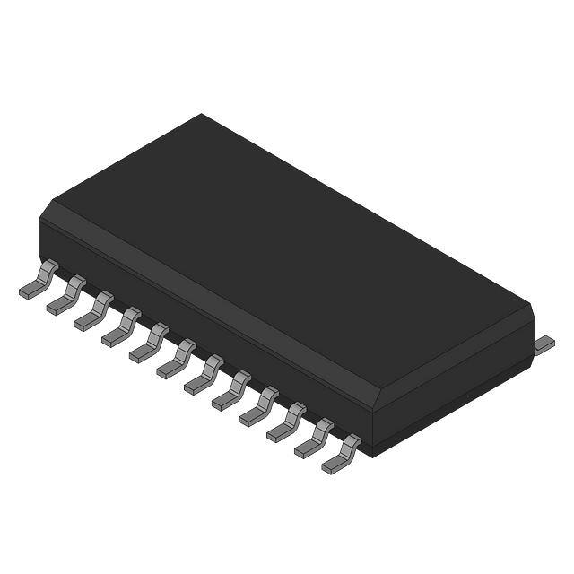
POST OFFICE BOX 1443 HOUSTON, TEXAS 77251−1443
•
�����������
�����������
������������
���������
����������
������ ���
�������
�����������
�����������
SDAS061C − APRIL 1982 − REVISED JANUARY 1995
switching characteristics (see Figure 1)
PARAMETER
FROM
(INPUT)
TO
(OUTPUT)
VCC = 4.5 V to 5.5 V,
CL = 50 pF,
R1 = 500 Ω,
R2 = 500 Ω,
TA = MIN to MAX†
SN74AS874
MIN
UNIT
MAX
fmax
125
tPLH
tPHL
3
8.5
MHz
CLK
Any Q
4
10.5
tPHL
CLR
Any Q
4
9.5
tPZH
tPZL
OE
Any Q
tPHZ
tPLZ
OE
Any Q
2
7
3
10.5
2
6
2
7.5
ns
ns
ns
ns
† For conditions shown as MIN or MAX, use the appropriate value specified under recommended operating conditions.
switching characteristics (see Figure 1)
PARAMETER
FROM
(INPUT)
TO
(OUTPUT)
VCC = 4.5 V to 5.5 V,
CL = 50 pF,
R1 = 500 Ω,
R2 = 500 Ω,
TA = MIN to MAX†
SN74AS876
MIN
UNIT
MAX
fmax
80
tPLH
tPHL
3
8.5
MHz
CLK
Any Q
4
10.5
tPHL
PRE
Any Q
4
9.5
tPZH
tPZL
OE
Any Q
tPHZ
tPLZ
OE
Any Q
2
7
3
11
2
7
2
7
ns
ns
ns
ns
† For conditions shown as MIN or MAX, use the appropriate value specified under recommended operating conditions.
•
POST OFFICE BOX 655303 DALLAS, TEXAS 75265
POST OFFICE BOX 1443 HOUSTON, TEXAS 77251−1443
•
7
�����������
�����������
������������
���������
����������
������ ���
�������
�����������
�����������
SDAS061C − APRIL 1982 − REVISED JANUARY 1995
PARAMETER MEASUREMENT INFORMATION
SERIES 54ALS/74ALS AND 54AS/74AS DEVICES
7V
RL = R1 = R2
VCC
S1
RL
R1
Test
Point
From Output
Under Test
CL
(see Note A)
From Output
Under Test
RL
Test
Point
CL
(see Note A)
CL
(see Note A)
LOAD CIRCUIT FOR
BI-STATE
TOTEM-POLE OUTPUTS
LOAD CIRCUIT
FOR OPEN-COLLECTOR OUTPUTS
3.5 V
Timing
Input
Test
Point
From Output
Under Test
LOAD CIRCUIT
FOR 3-STATE OUTPUTS
3.5 V
High-Level
Pulse
1.3 V
R2
1.3 V
1.3 V
0.3 V
0.3 V
tsu
Data
Input
tw
th
3.5 V
1.3 V
3.5 V
Low-Level
Pulse
1.3 V
0.3 V
1.3 V
0.3 V
VOLTAGE WAVEFORMS
PULSE DURATIONS
VOLTAGE WAVEFORMS
SETUP AND HOLD TIMES
3.5 V
Output
Control
(low-level
enabling)
1.3 V
1.3 V
0.3 V
tPZL
Waveform 1
S1 Closed
(see Note B)
tPLZ
3.5 V
Input
tPZH
1.3 V
0.3 V
tPHL
tPLH
VOH
In-Phase
Output
VOL
0.3 V
1.3 V
1.3 V
VOL
tPLH
tPHL
VOH
1.3 V
1.3 V
[3.5 V
1.3 V
tPHZ
Waveform 2
S1 Open
(see Note B)
1.3 V
VOH
Out-of-Phase
Output
(see Note C)
0.3 V
[0 V
1.3 V
1.3 V
VOL
VOLTAGE WAVEFORMS
PROPAGATION DELAY TIMES
VOLTAGE WAVEFORMS
ENABLE AND DISABLE TIMES, 3-STATE OUTPUTS
NOTES: A. CL includes probe and jig capacitance.
B. Waveform 1 is for an output with internal conditions such that the output is low except when disabled by the output control.
Waveform 2 is for an output with internal conditions such that the output is high except when disabled by the output control.
C. When measuring propagation delay items of 3-state outputs, switch S1 is open.
D. All input pulses have the following characteristics: PRR ≤ 1 MHz, tr = tf = 2 ns, duty cycle = 50%.
E. The outputs are measured one at a time with one transition per measurement.
Figure 1. Load Circuits and Voltage Waveforms
8
•
POST OFFICE BOX 655303 DALLAS, TEXAS 75265
POST OFFICE BOX 1443 HOUSTON, TEXAS 77251−1443
•
�PACKAGE OPTION ADDENDUM
www.ti.com
14-Oct-2022
PACKAGING INFORMATION
Orderable Device
Status
(1)
Package Type Package Pins Package
Drawing
Qty
Eco Plan
(2)
Lead finish/
Ball material
MSL Peak Temp
Op Temp (°C)
Device Marking
(3)
Samples
(4/5)
(6)
8401001LA
ACTIVE
CDIP
JT
24
1
Non-RoHS
& Green
SNPB
N / A for Pkg Type
-55 to 125
8401001LA
SNJ54ALS874BJT
Samples
SN54ALS874BJT
ACTIVE
CDIP
JT
24
1
Non-RoHS
& Green
SNPB
N / A for Pkg Type
-55 to 125
SN54ALS874BJT
Samples
SN74ALS874BDW
ACTIVE
SOIC
DW
24
25
RoHS & Green
NIPDAU
Level-1-260C-UNLIM
0 to 70
ALS874B
Samples
SN74ALS874BDWR
ACTIVE
SOIC
DW
24
2000
RoHS & Green
NIPDAU
Level-1-260C-UNLIM
0 to 70
ALS874B
Samples
SN74AS874DW
ACTIVE
SOIC
DW
24
25
RoHS & Green
NIPDAU
Level-1-260C-UNLIM
0 to 70
AS874
Samples
SNJ54ALS874BJT
ACTIVE
CDIP
JT
24
1
Non-RoHS
& Green
SNPB
N / A for Pkg Type
-55 to 125
8401001LA
SNJ54ALS874BJT
Samples
(1)
The marketing status values are defined as follows:
ACTIVE: Product device recommended for new designs.
LIFEBUY: TI has announced that the device will be discontinued, and a lifetime-buy period is in effect.
NRND: Not recommended for new designs. Device is in production to support existing customers, but TI does not recommend using this part in a new design.
PREVIEW: Device has been announced but is not in production. Samples may or may not be available.
OBSOLETE: TI has discontinued the production of the device.
(2)
RoHS: TI defines "RoHS" to mean semiconductor products that are compliant with the current EU RoHS requirements for all 10 RoHS substances, including the requirement that RoHS substance
do not exceed 0.1% by weight in homogeneous materials. Where designed to be soldered at high temperatures, "RoHS" products are suitable for use in specified lead-free processes. TI may
reference these types of products as "Pb-Free".
RoHS Exempt: TI defines "RoHS Exempt" to mean products that contain lead but are compliant with EU RoHS pursuant to a specific EU RoHS exemption.
Green: TI defines "Green" to mean the content of Chlorine (Cl) and Bromine (Br) based flame retardants meet JS709B low halogen requirements of