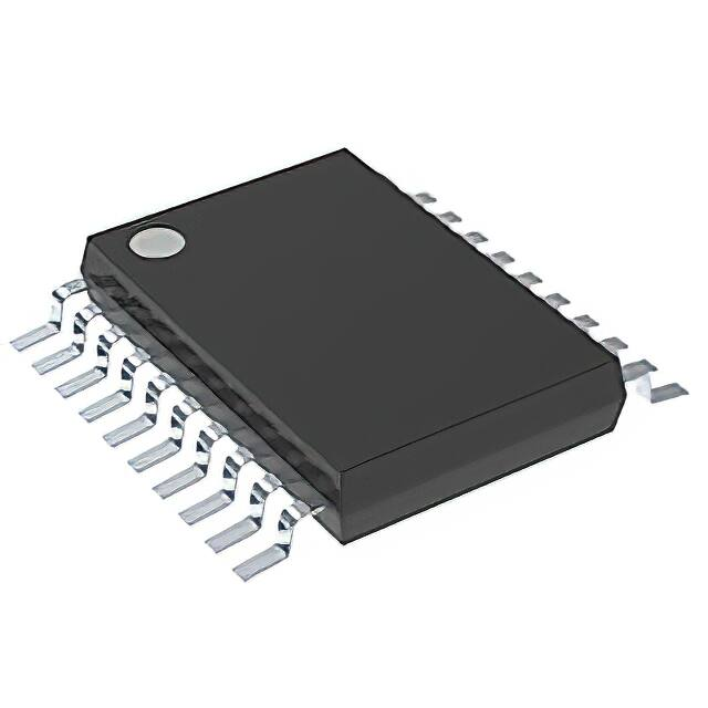
SN74ALVC244-EP
OCTAL BUFFER/DRIVER
WITH 3-STATE OUTPUTS
www.ti.com
SCES600A – AUGUST 2004 – REVISED OCTOBER 2004
FEATURES
•
•
•
•
•
•
•
•
•
(1)
PW PACKAGE
(TOP VIEW)
Controlled Baseline
– One Assembly/Test Site, One Fabrication
Site
Enhanced Diminishing Manufacturing
Sources (DMS) Support
Enhanced Product-Change Notification
Qualification Pedigree(1)
Operates From 1.65-V to 3.6-V VCC
Max tpd of 2.8 ns at 3.3-V VCC
±24-mA Output Drive at 3.3-V VCC
Latch-Up Performance Exceeds 250 mA Per
JESD 17
ESD Protection Exceeds JESD 22
– 2000-V Human-Body Model (A114-A)
– 200-V Machine Model (A115-A)
– 1000-V Charged-Device Model (C101)
1OE
1A1
2Y4
1A2
2Y3
1A3
2Y2
1A4
2Y1
GND
1
20
2
19
3
18
4
17
5
16
6
15
7
14
8
13
9
12
10
11
VCC
2OE
1Y1
2A4
1Y2
2A3
1Y3
2A2
1Y4
2A1
Component qualification in accordance with JEDEC and
industry standards to ensure reliable operation over an
extended temperature range. This includes, but is not limited
to, Highly Accelerated Stress Test (HAST) or biased 85/85,
temperature cycle, autoclave or unbiased HAST,
electromigration, bond intermetallic life, and mold compound
life. Such qualification testing should not be viewed as
justifying use of this component beyond specified
performance and environmental limits.
DESCRIPTION/ORDERING INFORMATION
This octal buffer/line driver is designed for 1.65-V to 3.6-V VCC operation.
The SN74ALVC244 is organized as two 4-bit line drivers with separate output-enable (OE) inputs. When OE is
low, the device passes data from the A inputs to the Y outputs. When OE is high, the outputs are in the
high-impedance state.
To ensure the high-impedance state during power up or power down, OE shall be tied to VCC through a pullup
resistor; the minimum value of the resistor is determined by the current-sinking capability of the driver.
ORDERING INFORMATION
PACKAGE (1)
TA
-40°C to 85°C
(1)
TSSOP - PW
Tape and reel
ORDERABLE PART NUMBER
SN74ALVC244IPWREP
TOP-SIDE MARKING
VA244IEP
Package drawings, standard packing quantities, thermal data, symbolization, and PCB design guidelines are available at
www.ti.com/sc/package.
Please be aware that an important notice concerning availability, standard warranty, and use in critical applications of Texas
Instruments semiconductor products and disclaimers thereto appears at the end of this data sheet.
PRODUCTION DATA information is current as of publication date.
Products conform to specifications per the terms of the Texas
Instruments standard warranty. Production processing does not
necessarily include testing of all parameters.
Copyright © 2004, Texas Instruments Incorporated
�SN74ALVC244-EP
OCTAL BUFFER/DRIVER
WITH 3-STATE OUTPUTS
www.ti.com
SCES600A – AUGUST 2004 – REVISED OCTOBER 2004
FUNCTION TABLE
(each buffer)
INPUTS
OE
A
OUTPUT
Y
L
H
H
L
L
L
H
X
Z
LOGIC DIAGRAM (POSITIVE LOGIC)
1OE
1A1
1A2
1A3
1A4
1
2OE
2
18
4
16
6
14
8
12
1Y1
2A1
1Y2
2A2
1Y3
2A3
1Y4
2A4
19
11
9
13
7
15
5
17
3
2Y1
2Y2
2Y3
2Y4
ABSOLUTE MAXIMUM RATINGS (1)
over operating free-air temperature range (unless otherwise noted)
MIN
MAX
VCC
Supply voltage range
-0.5
4.6
V
VI
Input voltage range (2)
-0.5
4.6
V
-0.5
VCC + 0.5
range (2) (3)
VO
Output voltage
IIK
Input clamp current
VI < 0
IOK
Output clamp current
VO < 0
IO
Continuous output current
Package thermal impedance (4)
Tstg
Storage temperature range
(1)
(2)
(3)
(4)
2
-65
V
-50
mA
-50
mA
±50
mA
±100
Continuous current through VCC or GND
θJA
UNIT
mA
83
°C/W
150
°C
Stresses beyond those listed under "absolute maximum ratings" may cause permanent damage to the device. These are stress ratings
only, and functional operation of the device at these or any other conditions beyond those indicated under "recommended operating
conditions" is not implied. Exposure to absolute-maximum-rated conditions for extended periods may affect device reliability.
The input negative-voltage and output voltage ratings may be exceeded if the input and output current ratings are observed.
This value is limited to 4.6 V maximum.
The package thermal impedance is calculated in accordance with JESD 51-7.
�SN74ALVC244-EP
OCTAL BUFFER/DRIVER
WITH 3-STATE OUTPUTS
www.ti.com
SCES600A – AUGUST 2004 – REVISED OCTOBER 2004
RECOMMENDED OPERATING CONDITIONS (1)
VCC
Supply voltage
VCC = 1.65 V to 1.95 V
VIH
High-level input voltage
MIN
MAX
1.65
3.6
Low-level input voltage
VI
Input voltage
VO
Output voltage
IOH
High-level output current
IOL
Low-level output current
∆t/∆v
Input transition rise or fall rate
TA
Operating free-air temperature
(1)
V
0.65 × VCC
VCC = 2.3 V to 2.7 V
1.7
VCC = 2.7 V to 3.6 V
2
V
0.35 × VCC
VCC = 1.65 V to 1.95 V
VIL
UNIT
VCC = 2.3 V to 2.7 V
0.7
VCC = 2.7 V to 3.6 V
0.8
V
0
3.6
V
0
VCC
V
VCC = 1.65 V
-4
VCC = 2.3 V
-12
VCC = 2.7 V
-12
VCC = 3 V
-24
VCC = 1.65 V
4
VCC = 2.3 V
12
VCC = 2.7 V
12
VCC = 3 V
24
-40
mA
mA
5
ns/V
85
°C
All unused inputs of the device must be held at VCC or GND to ensure proper device operation. Refer to the TI application report,
Implications of Slow or Floating CMOS Inputs, literature number SCBA004.
ELECTRICAL CHARACTERISTICS
over recommended operating free-air temperature range (unless otherwise noted)
PARAMETER
TEST CONDITIONS
IOH = -100 µA
1.65 V to 3.6 V
MIN TYP (1)
MAX
1.65 V
1.2
IOH = -6 mA
2.3 V
2
2.3 V
1.7
2.7 V
2.2
3V
2.4
IOH = -24 mA
3V
2
IOL = 100 µA
1.65 V to 3.6 V
0.2
IOL = 4 mA
1.65 V
0.45
IOL = 6 mA
2.3 V
0.4
2.3 V
0.7
IOH = -12 mA
IOL = 12 mA
IOL = 24 mA
UNIT
VCC - 0.2
IOH = -4 mA
VOH
VOL
VCC
V
2.7 V
0.4
3V
0.55
V
II
VI = VCC or GND
3.6 V
±5
µA
IOZ
VO = VCC or GND
3.6 V
±10
µA
ICC
VI = VCC or GND,
IO = 0
3.6 V
10
µA
One input at VCC - 0.6 V,
Other inputs at VCC or GND
750
µA
∆ICC
Ci
Co
(1)
Control inputs
Data inputs
Outputs
3 V to 3.6 V
VI = VCC or GND
3.3 V
VO = VCC or GND
3.3 V
4.5
4.5
7.5
pF
pF
All typical values are at VCC = 3.3 V, TA = 25°C.
3
�SN74ALVC244-EP
OCTAL BUFFER/DRIVER
WITH 3-STATE OUTPUTS
www.ti.com
SCES600A – AUGUST 2004 – REVISED OCTOBER 2004
SWITCHING CHARACTERISTICS
over recommended operating free-air temperature range (unless otherwise noted) (see Figure 1)
FROM
(INPUT)
TO
(OUTPUT)
tpd
A
ten
OE
tdis
OE
PARAMETER
VCC = 1.8 V
± 0.15 V
MIN
MAX
Y
1
Y
1.8
Y
1.8
VCC = 2.5 V
± 0.2 V
MIN
MAX
4.4
1
6.9
1.5
5.9
1
VCC = 2.7 V
MIN
VCC = 3.3 V
± 0.3 V
UNIT
MAX
MIN
MAX
3.1
3.1
1.1
2.8
ns
5.4
5.3
1.5
4.5
ns
4.1
4.4
1.7
4.2
ns
VCC = 1.8 V
VCC = 2.5 V
VCC = 3.3 V
TYP
TYP
TYP
22
23
26
1
1
1
OPERATING CHARACTERISTICS
TA = 25°C
TEST
CONDITIONS
PARAMETER
Cpd
4
Power dissipation capacitance
per buffer/driver
Outputs enabled
Outputs disabled
CL = 0, f = 10 MHz
UNIT
pF
�SN74ALVC244-EP
OCTAL BUFFER/DRIVER
WITH 3-STATE OUTPUTS
www.ti.com
SCES600A – AUGUST 2004 – REVISED OCTOBER 2004
PARAMETER MEASUREMENT INFORMATION
VLOAD
S1
RL
From Output
Under Test
Open
GND
CL
(see Note A)
RL
TEST
S1
tpd
tPLZ/tPZL
tPHZ/tPZH
Open
VLOAD
GND
LOAD CIRCUIT
INPUT
VCC
1.8 V ± 0.15 V
2.5 V ± 0.2 V
2.7 V
3.3 V ± 0.3 V
VI
tr/tf
VCC
VCC
2.7 V
2.7 V
≤2 ns
≤2 ns
≤2.5 ns
≤2.5 ns
VM
VLOAD
CL
RL
V∆
VCC/2
VCC/2
1.5 V
1.5 V
2 × VCC
2 × VCC
6V
6V
30 pF
30 pF
50 pF
50 pF
1 kΩ
500 Ω
500 Ω
500 Ω
0.15 V
0.15 V
0.3 V
0.3 V
tw
VI
Timing
Input
VM
VM
VM
0V
VOLTAGE WAVEFORMS
SETUP AND HOLD TIMES
VM
VM
0V
tPLH
Output
Control
(low-level
enabling)
tPLZ
VLOAD/2
VM
tPZH
VOH
VM
VOL
VOLTAGE WAVEFORMS
PROPAGATION DELAY TIMES
VM
0V
Output
Waveform 1
S1 at VLOAD
(see Note B)
tPHL
VM
VI
VM
tPZL
VI
Input
VOLTAGE WAVEFORMS
PULSE DURATION
th
VI
Data
Input
VM
0V
0V
tsu
Output
VI
VM
Input
Output
Waveform 2
S1 at GND
(see Note B)
VOL + V∆
VOL
tPHZ
VOH
VM
VOH − V∆
0V
VOLTAGE WAVEFORMS
ENABLE AND DISABLE TIMES
NOTES: A. CL includes probe and jig capacitance.
B. Waveform 1 is for an output with internal conditions such that the output is low, except when disabled by the output control.
Waveform 2 is for an output with internal conditions such that the output is high, except when disabled by the output control.
C. All input pulses are supplied by generators having the following characteristics: PRR ≤ 10 MHz, ZO = 50 Ω.
D. The outputs are measured one at a time, with one transition per measurement.
E. tPLZ and tPHZ are the same as tdis.
F. tPZL and tPZH are the same as ten.
G. tPLH and tPHL are the same as tpd.
H. All parameters and waveforms are not applicable to all devices.
Figure 1. Load Circuit and Voltage Waveforms
5
�PACKAGE OPTION ADDENDUM
www.ti.com
10-Dec-2020
PACKAGING INFORMATION
Orderable Device
Status
(1)
Package Type Package Pins Package
Drawing
Qty
Eco Plan
(2)
Lead finish/
Ball material
MSL Peak Temp
Op Temp (°C)
Device Marking
(3)
(4/5)
(6)
SN74ALVC244IPWREP
ACTIVE
TSSOP
PW
20
2000
RoHS & Green
NIPDAU
Level-1-260C-UNLIM
-40 to 85
VA244IEP
V62/04762-01XE
ACTIVE
TSSOP
PW
20
2000
RoHS & Green
NIPDAU
Level-1-260C-UNLIM
-40 to 85
VA244IEP
(1)
The marketing status values are defined as follows:
ACTIVE: Product device recommended for new designs.
LIFEBUY: TI has announced that the device will be discontinued, and a lifetime-buy period is in effect.
NRND: Not recommended for new designs. Device is in production to support existing customers, but TI does not recommend using this part in a new design.
PREVIEW: Device has been announced but is not in production. Samples may or may not be available.
OBSOLETE: TI has discontinued the production of the device.
(2)
RoHS: TI defines "RoHS" to mean semiconductor products that are compliant with the current EU RoHS requirements for all 10 RoHS substances, including the requirement that RoHS substance
do not exceed 0.1% by weight in homogeneous materials. Where designed to be soldered at high temperatures, "RoHS" products are suitable for use in specified lead-free processes. TI may
reference these types of products as "Pb-Free".
RoHS Exempt: TI defines "RoHS Exempt" to mean products that contain lead but are compliant with EU RoHS pursuant to a specific EU RoHS exemption.
Green: TI defines "Green" to mean the content of Chlorine (Cl) and Bromine (Br) based flame retardants meet JS709B low halogen requirements of
很抱歉,暂时无法提供与“SN74ALVC244IPWREP”相匹配的价格&库存,您可以联系我们找货
免费人工找货