Product
Folder
Sample &
Buy
Support &
Community
Tools &
Software
Technical
Documents
SN74AUP1T34-Q1
SCES852A – DECEMBER 2013 – REVISED APRIL 2016
SN74AUP1T34-Q1 1-Bit Unidirectional Voltage-Level Translator
1 Features
2 Applications
•
•
•
•
•
•
1
•
•
•
•
•
•
•
•
•
•
Qualified for Automotive Applications
– AEC-Q100 Qualified
– Device Temperature Grade 1: –40°C to 125°C
Ambient Operating Temperature
– Device HBM ESD Classification Level 3A
– Device CDM ESD Classification Level C5
Wide Operating VCC Range of 0.9 V to 3.6 V
Balanced Propagation Delays: tPLH = tPHL
(1.8-V to 3.3-V Translation Typical)
Low Static-Power Consumption: Maximum of 5-µA
ICC
±6-mA Output Drive at 3 V
Ioff Supports Partial Power-Down-Mode Operation
VCC Isolation Feature – If VCCA Input Is at GND,
B Port Is in the High-Impedance state
Input Hysteresis Allows Slow Input Transition and
Better Switching Noise Immunity at Input
ESD Protection Exceeds JESD 22
5000-V Human-Body Model (AEC-Q100-002-E)
Latch-Up Performance Meets
100 mA Per Q100-004-D
Automotive
Enterprise
Industrial
Personal Electronics
Telecommunications
3 Description
The SN74AUP1T34-Q1 device is a 1-bit noninverting
translator that uses two separate configurable powersupply rails. It is a unidirectional translator from A to
B. The A port is designed to track VCCA. VCCA accepts
supply voltages from 0.9 V to 3.6 V. The B port is
designed to track VCCB. VCCB accepts supply voltages
from 0.9 V to 3.6 V. This allows for low-voltage
translation between 1-V, 1.2-V, 1.5-V, 1.8-V, 2.5-V,
and 3.3-V voltage nodes. The SN74AUP1T34-Q1 is
also
fully
specified
for
partial-power-down
applications using Ioff. The Ioff circuitry disables the
outputs, preventing damaging current backflow
through the device when it is powered down.
The VCC isolation feature ensures that if VCCA input
is at GND, the B port is in the high-impedance state.
If VCCB input is at GND, any input to the A side does
not cause the leakage current even floating.
Device Information(1)
PART NUMBER
SN74AUP1T34-Q1
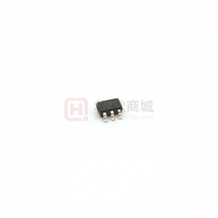
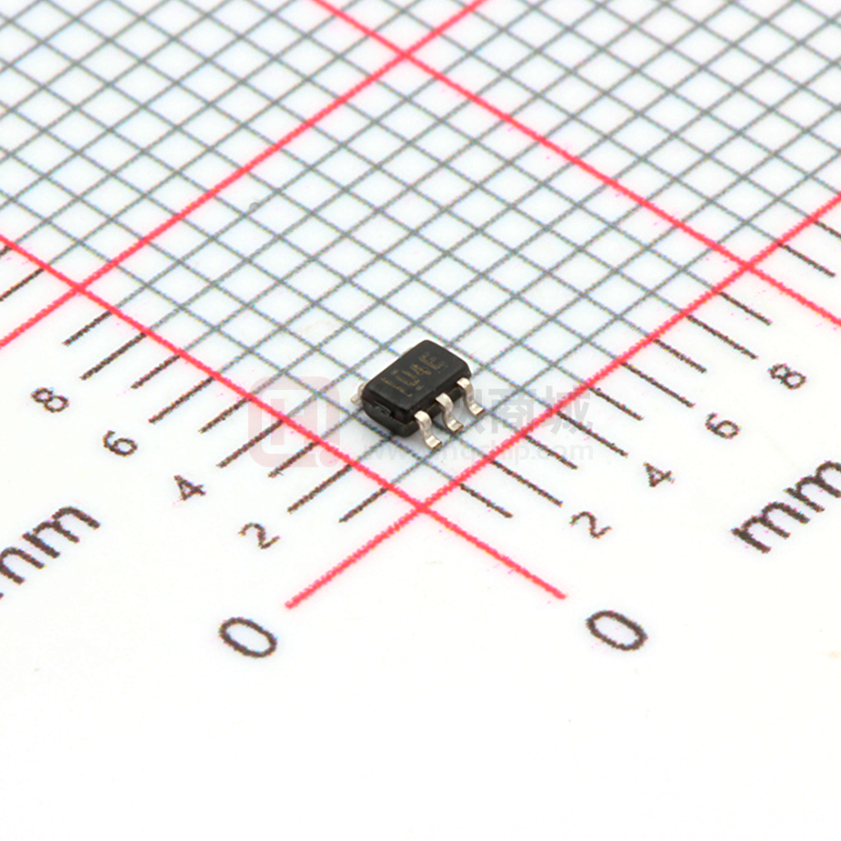
PACKAGE
SC70 (5)
BODY SIZE (NOM)
2.00 mm × 1.25 mm
(1) For all available packages, see the orderable addendum at
the end of the data sheet.
Example Application Diagram
Camera Module 1
ADAS Host
Processor
Control Output
SN74AUP1T34-Q1
Camera Module 2
To Multiple Loads
Camera Module 3
Copyright © 2016, Texas Instruments Incorporated
1
An IMPORTANT NOTICE at the end of this data sheet addresses availability, warranty, changes, use in safety-critical applications,
intellectual property matters and other important disclaimers. PRODUCTION DATA.
�SN74AUP1T34-Q1
SCES852A – DECEMBER 2013 – REVISED APRIL 2016
www.ti.com
Table of Contents
1
2
3
4
5
6
7
8
Features ..................................................................
Applications ...........................................................
Description .............................................................
Revision History.....................................................
Pin Configuration and Functions .........................
Specifications.........................................................
1
1
1
2
3
3
6.1
6.2
6.3
6.4
6.5
6.6
3
3
4
4
5
6
Absolute Maximum Ratings ......................................
ESD Ratings..............................................................
Recommended Operating Conditions ......................
Thermal Information ..................................................
AC Electrical Characteristics.....................................
Typical Characteristics ..............................................
Parameter Measurement Information .................. 6
Detailed Description .............................................. 7
8.1 Overview ................................................................... 7
8.2 Functional Block Diagram ......................................... 7
8.3 Feature Description................................................... 7
8.4 Device Functional Modes.......................................... 7
9
Application and Implementation .......................... 8
9.1 Application Information.............................................. 8
9.2 Typical Application ................................................... 8
10 Power Supply Recommendations ....................... 9
11 Layout................................................................... 10
11.1 Layout Guidelines ................................................. 10
11.2 Layout Example .................................................... 10
12 Device and Documentation Support ................. 11
12.1
12.2
12.3
12.4
Community Resources..........................................
Trademarks ...........................................................
Electrostatic Discharge Caution ............................
Glossary ................................................................
11
11
11
11
13 Mechanical, Packaging, and Orderable
Information ........................................................... 11
4 Revision History
NOTE: Page numbers for previous revisions may differ from page numbers in the current version.
Changes from Original (December 2013) to Revision A
Page
•
Added ESD Ratings table, Feature Description section, Device Functional Modes, Application and Implementation
section, Power Supply Recommendations section, Layout section, Device and Documentation Support section, and
Mechanical, Packaging, and Orderable Information section. ................................................................................................. 1
•
Removed Ordering Information table .................................................................................................................................... 1
2
Submit Documentation Feedback
Copyright © 2013–2016, Texas Instruments Incorporated
Product Folder Links: SN74AUP1T34-Q1
�SN74AUP1T34-Q1
www.ti.com
SCES852A – DECEMBER 2013 – REVISED APRIL 2016
5 Pin Configuration and Functions
DCK Package
5-Pin SC70
Top View
V
CCA
1
A
2
GND
3
5
V
4
B
CCB
Pin Functions
PIN
NAME
I/O
NO.
DESCRIPTION
A
2
I
Input Port. Referenced to VCCA.
B
4
O
Output Port. Referenced to VCCB.
GND
3
—
Ground.
VCCA
1
—
Input Port DC Power Supply.
VCCB
5
—
Output Port DC Power Supply.
6 Specifications
6.1 Absolute Maximum Ratings
over operating free-air temperature range (unless otherwise noted)
MIN
MAX
UNIT
VCCA,
VCCB
Supply voltage
–0.3
4
V
VI
Input voltage
–0.5
4.6
V
Voltage applied to any output in the high-impedance or power-off state
–0.5
4.6
Voltage applied to any output in the high or low state
–0.5
4.6
VO
V
IIK
Input clamp current
VI < 0
–50
mA
IOK
Output clamp current
VO < 0
–50
mA
IO
Continuous output current
±50
mA
Continuous current through VCCA or GND
±100
mA
150
°C
Tstg
Storage temperature
–65
6.2 ESD Ratings
VALUE
V(ESD)
(1)
(2)
Electrostatic
discharge
Human-body model (HBM), per ANSI/ESDA/JEDEC JS-001
(1)
, Classification 3A
UNIT
5000
Charged-device model (CDM), per JEDEC specification JESD22-C101 (2),
Classification C5
750
V
JEDEC document JEP155 states that 500-V HBM allows safe manufacturing with a standard ESD control process.
JEDEC document JEP157 states that 250-V CDM allows safe manufacturing with a standard ESD control process.
Submit Documentation Feedback
Copyright © 2013–2016, Texas Instruments Incorporated
Product Folder Links: SN74AUP1T34-Q1
3
�SN74AUP1T34-Q1
SCES852A – DECEMBER 2013 – REVISED APRIL 2016
www.ti.com
6.3 Recommended Operating Conditions
over operating free-air temperature range (unless otherwise noted)
PARAMETER
VCCA,
VCCB
Supply voltage
VIH
High-level input voltage
VIL
Low-level input voltage
Δt/Δv
Input transition rise or fall
rate
TA
Operating free-air
temperature
TEST CONDITIONS
Control inputs
Ioff
A or B port
ICCA
0.9
3.6
0.9 V to 1.95 V
0.9 V to 1.95 V
0.65 × VCCA
2.3 V to 2.7 V
0.9 V to 3.6 V
1.6
3 V to 3.6 V
0.9 V to 3.6 V
2
V
0.9 V to 1.95 V
0.3 × VCCA
0.9 V to 1.95 V
0.35 × VCCA
2.3 V to 2.7 V
0.9 V to 3.6 V
0.7
3 V to 3.6 V
0.9 V to 3.6 V
0.9
3 V to 3.6 V
0.9 V to 3.6 V
200
ns/V
125
°C
0.9 V to 3.6 V
VCCB – 0.2
0.9 V to 1 V
0.75 × VCCB
1.2 V
1.2 V
1
1.65 V
1.65 V
1.32
IOH = –3 mA
2.3 V
2.3 V
1.9
IOH = –6 mA
3V
3V
2.72
IOL = 100 µA
0.9 V to 3.6 V
0.9 V to 3.6 V
IOL = 0.25 mA
0.9 V to 1 V
0.9 V 1 V
IOL = 1.5 mA
1.2 V
1.2 V
0.3 × VCCB
1.65 V
1.65 V
0.31
IOL = 3 mA
2.3 V
2.3 V
0.31
IOL = 6 mA
3V
3V
0.31
0.9 V to 3.6 V
0.9 V to 3.6 V
±1
0V
0 V to 3.6 V
±5
0 V to 3.6 V
0V
±5
0.9 V to 3.6 V
0.9 V to 3.6 V
2.7
0.9 V to 3.6 V
VCCA
2
0V
0 V to 3.6 V
1
VI = VIL
VI = VCCA or GND
VI or VO = 0 to 3.6 V
ICCB
VI = VCCI or GND, IO = 0 mA
ICCA + ICCB
VI = VCCI or GND, IO = 0 mA
A or B port
V
0.9 V
0.9 V to 1 V
VI = VIH
UNIT
1 V to 1.95 V
0.9 V to 3.6 V
VI = VCCI or GND, IO = 0 mA
Cio
MAX
IOH = –0.25 mA
IOL = 2 mA
II
MIN
IOH = –100 µA
IOH = –2 mA
VOL
VCCB
–40
IOH = –1.5 mA
VOH
VCCA
V
V
0.1
0.1
0 V to 3.6 V
0V
0.9 V to 3.6 V
0.9 V to 3.6 V
V
µA
µA
µA
1
2.7
0.9 V to 3.6 V
VCCA
2
0V
0 V to 3.6 V
1
0 V to 3.6 V
0V
0.9 V to 3.6 V
0.9 V to 3.6 V
3.3 V
3.3 V
µA
1
5.4
µA
4
pF
6.4 Thermal Information
SN74AUP1T34-Q1
THERMAL METRIC (1)
DCK (SC70)
UNIT
5 PINS
RθJA
Junction-to-ambient thermal resistance
301.9
°C/W
RθJC(top)
Junction-to-case (top) thermal resistance
113
°C/W
RθJB
Junction-to-board thermal resistance
79.1
°C/W
ψJT
Junction-to-top characterization parameter
3.9
°C/W
ψJB
Junction-to-board characterization parameter
78.3
°C/W
(1)
4
For more information about traditional and new thermal metrics, see the Semiconductor and IC Package Thermal Metrics application
report, SPRA953.
Submit Documentation Feedback
Copyright © 2013–2016, Texas Instruments Incorporated
Product Folder Links: SN74AUP1T34-Q1
�SN74AUP1T34-Q1
www.ti.com
SCES852A – DECEMBER 2013 – REVISED APRIL 2016
6.5 AC Electrical Characteristics
over operating free-air temperature range (unless otherwise noted)
PARAMETER
tPLH/tPHL
tPLH/tPHL
tPLH/tPHL
tPLH/tPHL
CL
VCCB = 0.9 V
VCCA
TYP
VCCB = 1.2 V
MAX
25
TYP
VCCB = 1.65 V
MAX
18
TYP
VCCB = 2.3 V
MAX
TYP
16.2
MAX
16.3
VCCB = 3 V
TYP
MAX
5 pF
0.9 V
5 pF
1.2 V
5 pF
1.65 V
5 pF
2.3 V
5 pF
3V
10 pF
0.9 V
16.8
10 pF
1.2 V
43.22
12.33
9.57
8.81
8.61
10 pF
1.65 V
40.44
9.21
6.57
5.6
4.73
10 pF
2.3 V
41.56
8.3
5.54
4.42
4.07
10 pF
3V
15 pF
0.9 V
15 pF
1.2 V
43.87
16.2
11.8
11
11
15 pF
1.65 V
40.78
14.7
8.8
7.1
6.4
15 pF
2.3 V
41.79
14.9
7.6
5.88
5.27
15 pF
3V
30 pF
0.9 V
30 pF
1.2 V
45.65
15.1
12.37
11.61
30 pF
1.65 V
41.72
12.18
8.15
6.94
6.1
30 pF
2.3 V
42.44
12.35
7.25
5.55
4.97
30 pF
3V
43.69
11.6
6.92
4.95
4.35
42.5
24.9
23.2
22.6
22.5
40
10.7
8.84
8.08
7.88
41.3
8.02
5.73
4.92
4.2
42.5
28.9
7.61
19.8
42.81
30.6
43.09
3.65
18
7.87
21.6
32.1
4.5
17.9
4.8
19.7
16.2
21.3
6.98
3.39
ns
3.36
20.3
5.4
18.7
ns
18.5
3.8
19.6
UNIT
18
ns
4.7
18.3
11.41
ns
VIH
Input (An)
Vm
Vm
0V
tPLH
tPLH
Vm
Output(Bn)
VOH
Vm
VOL
VMI =VIH/2; VMO= VCCB/2
tR = tF = 2.0 ns, 10% to 90%; f = 1 MHz; tW = 500 ns
Figure 1. Waveform 1 - Propagation Delays
Submit Documentation Feedback
Copyright © 2013–2016, Texas Instruments Incorporated
Product Folder Links: SN74AUP1T34-Q1
5
�SN74AUP1T34-Q1
SCES852A – DECEMBER 2013 – REVISED APRIL 2016
www.ti.com
6.6 Typical Characteristics
0.600
Low Level Output Voltage [V]
0.500
0.400
0.300
0.200
VCCB = 1.0V
VCCB = 1.2V
VCCB = 1.5V
0.100
VCCB = 1.8V
VCCB = 2.5V
VCCB = 3.3V
0.000
0.00
5.00
10.00
15.00
20.00
25.00
30.00
Low Level Output Current [mA] with VIL = 0V
C001
Figure 2. Low Level Output Voltage vs Low Level Output Current
7 Parameter Measurement Information
VCC
Pulse
Generator
DUT
CL
RL
TEST
tPLH, tPHL
CL = 5 pF, 10 pF, 15 pF, 30 pF or equivalent (includes probe and jig capacitance)
RL = 1 MΩ or equivalent
ZOUT of pulse generator = 50 Ω
Figure 3. AC (Propagation Delay) Test Circuit
6
Submit Documentation Feedback
Copyright © 2013–2016, Texas Instruments Incorporated
Product Folder Links: SN74AUP1T34-Q1
�SN74AUP1T34-Q1
www.ti.com
SCES852A – DECEMBER 2013 – REVISED APRIL 2016
8 Detailed Description
8.1 Overview
The SN74AUP1T34-Q1 is a unidirectional, single-bit, dual-supply, noninverting voltage-level translator. Pin A,
which is referenced to VCCA, receives the signal that is to be level translated. Pin B, which is referenced to VCCB,
transmits the level translated signal. Both supply pins VCCA and VCCB support a voltage range from 0.9 V to
3.6 V.
8.2 Functional Block Diagram
VCCA
A
VCCB
2
4
B
Copyright © 2016, Texas Instruments Incorporated
8.3 Feature Description
8.3.1 Fully Configurable Dual-Rail Design
Both VCCA and VCCB can be supplied at any voltage from 0.9 V to 3.6 V, making the device suitable for translating
between any of the voltage nodes (1 V, 1.2 V, 1.8 V, 2.5 V, and 3.3 V).
8.3.2 Partial-Power-Down Mode Operation
Ioff circuitry disables the outputs, preventing damaging current backflow through the SN74AUP1T34-Q1 when it is
powered down. This can occur in applications where subsections of a system are powered down (partial-powerdown) to reduce power consumption.
8.3.3 VCC Isolation
The VCC isolation feature ensures that if either VCCA or VCCB are at GND (or < 0.4 V), both ports A and B are set
to a high-impedance state, preventing false logic levels from being presented to either bus.
8.3.4 Input Hysteresis
Input hysteresis allows the input to support slew rates as slow as 200 ns/V, improving switching noise immunity.
8.4 Device Functional Modes
Table 1 lists the functional modes of the SN74AUP1T34-Q1.
Table 1. Function Table
INPUT
OUTPUT
A PORT
B PORT
L
L
H
H
Submit Documentation Feedback
Copyright © 2013–2016, Texas Instruments Incorporated
Product Folder Links: SN74AUP1T34-Q1
7
�SN74AUP1T34-Q1
SCES852A – DECEMBER 2013 – REVISED APRIL 2016
www.ti.com
9 Application and Implementation
NOTE
Information in the following applications sections is not part of the TI component
specification, and TI does not warrant its accuracy or completeness. TI’s customers are
responsible for determining suitability of components for their purposes. Customers should
validate and test their design implementation to confirm system functionality.
9.1 Application Information
The SN74AUP1T34-Q1 can be used in level-translation applications for interfacing devices or systems operating
at different interface voltages with one another.
9.2 Typical Application
1.0V
3.3V
1.0 µF
0.1 µF
0.1 µF
VCCA
VDD (1.0V)
1.0V Controller
1.0 µF
VCCB
VDD (3.3V)
SN74AUP1T34-Q1
Signal
A
GND
3.3V System
B
Signal
GND
GND
Copyright © 2016, Texas Instruments Incorporated
Figure 4. Typical Application Example
9.2.1 Design Requirements
Table 2 lists the design requirements of the SN74AUP1T34-Q1.
Table 2. Design Parameters
DESIGN PARAMETER
EXAMPLE VALUE
Input Voltage Range
0.9 V to 3.6 V
Output Voltage Range
0.9 V to 3.6 V
9.2.2 Detailed Design Procedure
To begin the design process, determine the following:
• Input voltage range
– Use the supply voltage of the device that is driving the SN74AUP1T34-Q1 device to determine the input
voltage range. For a valid logic-high, the value must exceed the VIH of the input port. For a valid logic low
the value must be less than the VIL of the input port.
• Output voltage range
– Use the supply voltage of the device that the SN74AUP1T34-Q1 device is driving to determine the output
voltage range.
8
Submit Documentation Feedback
Copyright © 2013–2016, Texas Instruments Incorporated
Product Folder Links: SN74AUP1T34-Q1
�SN74AUP1T34-Q1
www.ti.com
SCES852A – DECEMBER 2013 – REVISED APRIL 2016
9.2.3 Application Curve
Figure 5. 10 MHz Up Translation (0.9 V to 3.6 V)
10 Power Supply Recommendations
Connect ground before applying either VCCA or VCCB. There is no specific power sequence requirement for the
SN74AUP1T34. VCCA or VCCB may be powered up first, and VCCA or VCCB may be powered down first.
Submit Documentation Feedback
Copyright © 2013–2016, Texas Instruments Incorporated
Product Folder Links: SN74AUP1T34-Q1
9
�SN74AUP1T34-Q1
SCES852A – DECEMBER 2013 – REVISED APRIL 2016
www.ti.com
11 Layout
11.1 Layout Guidelines
To
•
•
•
ensure reliability of the device, TI recommends following common printed-circuit board layout guidelines.
Bypass capacitors must be used on power supplies.
Short trace lengths must be used to avoid excessive loading.
Placing pads on the signal paths for loading capacitors or pullup resistors helps adjust rise and fall times of
signals depending on the system requirements.
11.2 Layout Example
LEGEND
Polygonal Copper Pour
VIA to Power Plane (Inner Layer)
VIA to GND Plane (Inner Layer)
Bypass Capacitor
Bypass Capacitor
From Source
1
VCCA
2
A
3
GND
VCCB
5
B
4
To Destination
SN74AUP1T34-Q1DCK
(Top View)
Figure 6. Example Layout
10
Submit Documentation Feedback
Copyright © 2013–2016, Texas Instruments Incorporated
Product Folder Links: SN74AUP1T34-Q1
�SN74AUP1T34-Q1
www.ti.com
SCES852A – DECEMBER 2013 – REVISED APRIL 2016
12 Device and Documentation Support
12.1 Community Resources
The following links connect to TI community resources. Linked contents are provided "AS IS" by the respective
contributors. They do not constitute TI specifications and do not necessarily reflect TI's views; see TI's Terms of
Use.
TI E2E™ Online Community TI's Engineer-to-Engineer (E2E) Community. Created to foster collaboration
among engineers. At e2e.ti.com, you can ask questions, share knowledge, explore ideas and help
solve problems with fellow engineers.
Design Support TI's Design Support Quickly find helpful E2E forums along with design support tools and
contact information for technical support.
12.2 Trademarks
E2E is a trademark of Texas Instruments.
All other trademarks are the property of their respective owners.
12.3 Electrostatic Discharge Caution
These devices have limited built-in ESD protection. The leads should be shorted together or the device placed in conductive foam
during storage or handling to prevent electrostatic damage to the MOS gates.
12.4 Glossary
SLYZ022 — TI Glossary.
This glossary lists and explains terms, acronyms, and definitions.
13 Mechanical, Packaging, and Orderable Information
The following pages include mechanical, packaging, and orderable information. This information is the most
current data available for the designated devices. This data is subject to change without notice and revision of
this document. For browser-based versions of this data sheet, refer to the left-hand navigation.
Submit Documentation Feedback
Copyright © 2013–2016, Texas Instruments Incorporated
Product Folder Links: SN74AUP1T34-Q1
11
�PACKAGE OPTION ADDENDUM
www.ti.com
6-Feb-2020
PACKAGING INFORMATION
Orderable Device
Status
(1)
SN74AUP1T34QDCKRQ1
ACTIVE
Package Type Package Pins Package
Drawing
Qty
SC70
DCK
5
3000
Eco Plan
Lead/Ball Finish
MSL Peak Temp
(2)
(6)
(3)
Green (RoHS
& no Sb/Br)
NIPDAU
Level-1-260C-UNLIM
Op Temp (°C)
Device Marking
(4/5)
-40 to 125
U4E
(1)
The marketing status values are defined as follows:
ACTIVE: Product device recommended for new designs.
LIFEBUY: TI has announced that the device will be discontinued, and a lifetime-buy period is in effect.
NRND: Not recommended for new designs. Device is in production to support existing customers, but TI does not recommend using this part in a new design.
PREVIEW: Device has been announced but is not in production. Samples may or may not be available.
OBSOLETE: TI has discontinued the production of the device.
(2)
RoHS: TI defines "RoHS" to mean semiconductor products that are compliant with the current EU RoHS requirements for all 10 RoHS substances, including the requirement that RoHS substance
do not exceed 0.1% by weight in homogeneous materials. Where designed to be soldered at high temperatures, "RoHS" products are suitable for use in specified lead-free processes. TI may
reference these types of products as "Pb-Free".
RoHS Exempt: TI defines "RoHS Exempt" to mean products that contain lead but are compliant with EU RoHS pursuant to a specific EU RoHS exemption.
Green: TI defines "Green" to mean the content of Chlorine (Cl) and Bromine (Br) based flame retardants meet JS709B low halogen requirements of


 工商网监
湘ICP备2023018690号
工商网监
湘ICP备2023018690号
