����������
����������
���
�
����������
��
���������
����
����
��
�������
SCBS026C − NOVEMBER 1988 − REVISED APRIL 1994
•
•
•
•
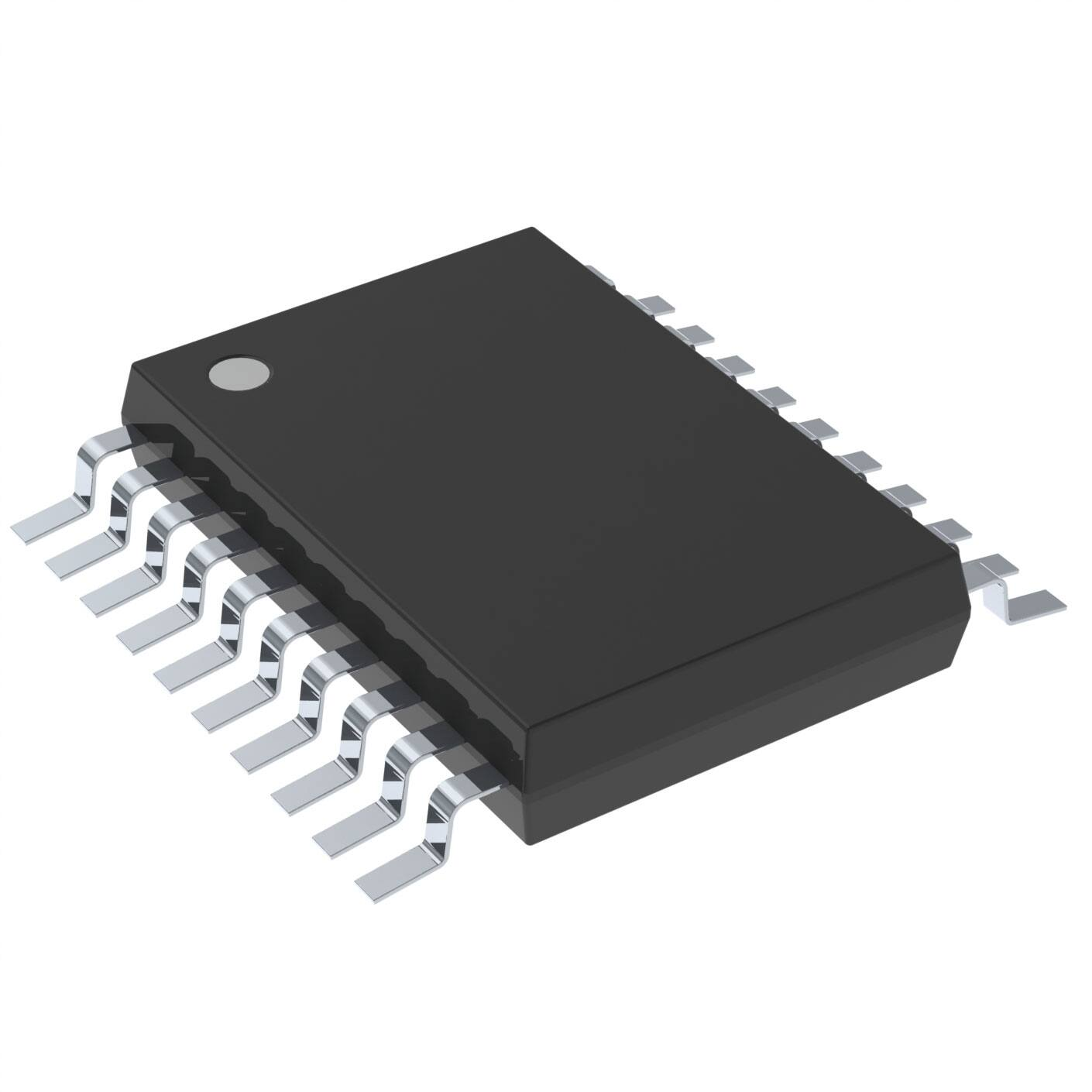
SN54BCT543 . . . JT OR W PACKAGE
SN74BCT543 . . . DW OR NT PACKAGE
(TOP VIEW)
State-of-the-Art BiCMOS Design
Significantly Reduces ICCZ
3-State True Outputs
Back-to-Back Registers for Storage
ESD Protection Exceeds 2000 V
Per MIL-STD-883C, Method 3015
Package Options Include Plastic
Small-Outline Packages (DW), Ceramic
Chip Carriers (FK) and Flatpacks (W), and
Plastic and Ceramic 300-mil DIPs (JT, NT)
LEBA
OEBA
A1
A2
A3
A4
A5
A6
A7
A8
CEAB
GND
description
The ′BCT543 octal transceiver contains two sets
of D-type latches for temporary storage of data
flowing in either direction. Separate latch-enable
(LEAB or LEBA) and output-enable (OEAB or
OEBA) inputs are provided for each register to
permit independent control in either direction of
data flow.
1
24
2
23
3
22
4
21
5
20
6
19
7
18
8
17
9
16
10
15
11
14
12
13
VCC
CEBA
B1
B2
B3
B4
B5
B6
B7
B8
LEAB
OEAB
A1
OEBA
LEBA
NC
VCC
SN54BCT543 . . . FK PACKAGE
(TOP VIEW)
The A-to-B enable (CEAB) input must be low in
order to enter data from A or to output data from
B. If CEAB is low and LEAB is low, the A-to-B
latches are transparent; a subsequent low-to-high
transition of LEAB puts the A latches in the storage
mode. With CEAB and OEAB both low, the 3-state
B outputs are active and reflect the data present
at the output of the A latches. Data flow from B to
A is similar but requires using the CEBA, LEBA,
and OEBA inputs.
5
A2
A3
A4
NC
A5
A6
A7
3 2 1 28 27 26
25
4
6
24
7
23
8
22
9
21
10
20
11
19
12 13 14 15 16 17 18
B2
B3
B4
NC
B5
B6
B7
A8
CEAB
GND
NC
OEAB
LEAB
B8
The SN54BCT543 is characterized for operation
over the full military temperature range of − 55°C
to 125°C. The SN74BCT543 is characterized for
operation from 0°C to 70°C.
CEBA
B1
•
NC − No internal connection
FUNCTION TABLE†
INPUTS
OEAB
A
OUTPUT
B
X
X
X
Z
X
H
X
Z
L
H
L
X
L
L
L
L
B0‡
L
L
L
L
H
CEAB
LEAB
H
X
H
† A-to-B data flow is shown; B-to-A flow control is the
same except that it uses CEBA, LEBA, and OEBA.
‡ Output level before the indicated steady-state input
conditions were established.
Copyright 1994, Texas Instruments Incorporated
���������� �
�
������!"��� �# $%��&�" !# �� '%()�$!"��� *!"&+
���*%$"# $������ "� #'&$���$!"���# '&� ",& "&��# �� �&-!# ��#"�%�&�"#
#"!�*!�* .!��!�"/+ ���*%$"��� '��$&##��0 *�&# ��" �&$&##!��)/ ��$)%*&
"&#"��0 �� !)) '!�!�&"&�#+
• DALLAS, TEXAS 75265
• HOUSTON, TEXAS 77251−1443
POST OFFICE BOX 655303
POST OFFICE BOX 1443
2−1
�����������
����������
���
�
����������
��
���������
����
����
��
�������
SCBS026C − NOVEMBER 1988 − REVISED APRIL 1994
logic symbol†
2
OEBA
23
CEBA
1
LEBA
13
OEAB
11
CEAB
14
LEAB
A1
A2
A3
A4
A5
A6
A7
A8
1EN3
G1
1C5
2EN4
G2
2C6
3
4
3
1
5D
6D
1
4
22
21
5
20
6
19
7
18
8
17
9
16
10
15
B1
B2
B3
B4
B5
B6
B7
B8
† This symbol is in accordance with ANSI/IEEE Std 91-1984 and IEC Publication 617-12.
logic diagram (positive logic)
OEBA
CEBA
LEBA
OEAB
CEAB
LEAB
A1
2
23
1
13
11
14
C1
3
1D
C1
1D
To Seven Other Channels
Pin numbers shown are for the DW, JT, NT, and W packages.
2−2
•
POST OFFICE BOX 655303 DALLAS, TEXAS 75265
POST OFFICE BOX 1443 HOUSTON, TEXAS 77251−1443
•
22
B1
�����������
����������
���
�
����������
��
���������
����
����
��
�������
SCBS026C − NOVEMBER 1988 − REVISED APRIL 1994
absolute maximum ratings over operating free-air temperature range (unless otherwise noted)†
Supply voltage range, VCC . . . . . . . . . . . . . . . . . . . . . . . . . . . . . . . . . . . . . . . . . . . . . . . . . . . . . . . . . . − 0.5 V to 7 V
Input voltage range: Control inputs (see Note 1) . . . . . . . . . . . . . . . . . . . . . . . . . . . . . . . . . . . . . . . . − 0.5 V to 7 V
I/O ports (see Note 1) . . . . . . . . . . . . . . . . . . . . . . . . . . . . . . . . . . . . . . . . . . − 0.5 V to 5.5 V
Voltage range applied to any output in the disabled or power-off state, VO . . . . . . . . . . . . . . . . . − 0.5 V to 7 V
Voltage range applied to any output in the high state, VO . . . . . . . . . . . . . . . . . . . . . . . . . . . . . . . − 0.5 V to VCC
Input clamp current, IIK . . . . . . . . . . . . . . . . . . . . . . . . . . . . . . . . . . . . . . . . . . . . . . . . . . . . . . . . . . . . . . . . . . −30 mA
Current into any output in the low state: SN54BCT543 . . . . . . . . . . . . . . . . . . . . . . . . . . . . . . . . . . . . . . . . 96 mA
SN74BCT543 . . . . . . . . . . . . . . . . . . . . . . . . . . . . . . . . . . . . . . . 128 mA
Operating free-air temperature range: SN54BCT543 . . . . . . . . . . . . . . . . . . . . . . . . . . . . . . . . − 55°C to 125°C
SN74BCT543 . . . . . . . . . . . . . . . . . . . . . . . . . . . . . . . . . . . . 0°C to 70°C
Storage temperature range . . . . . . . . . . . . . . . . . . . . . . . . . . . . . . . . . . . . . . . . . . . . . . . . . . . . . . . . − 65°C to 150°C
† Stresses beyond those listed under “absolute maximum ratings” may cause permanent damage to the device. These are stress ratings only, and
functional operation of the device at these or any other conditions beyond those indicated under “recommended operating conditions” is not
implied. Exposure to absolute-maximum-rated conditions for extended periods may affect device reliability.
NOTE 1: The input and output voltage ratings may be exceeded if the input and output current ratings are observed.
recommended operating conditions
SN54BCT543
SN74BCT543
MIN
NOM
MAX
MIN
NOM
MAX
4.5
5
5.5
4.5
5
5.5
VCC
VIH
Supply voltage
VIL
IIK
Low-level input voltage
Input clamp current
IOH
IOL
High-level output current
Low-level output current
48
TA
Operating free-air temperature
High-level input voltage
2
2
0.8
−55
•
POST OFFICE BOX 655303 DALLAS, TEXAS 75265
POST OFFICE BOX 1443 HOUSTON, TEXAS 77251−1443
•
UNIT
V
V
0.8
V
−18
−18
mA
−12
−15
mA
64
mA
70
°C
125
0
2−3
�����������
����������
���
�
����������
��
���������
����
����
��
�������
SCBS026C − NOVEMBER 1988 − REVISED APRIL 1994
electrical characteristics over recommended operating free-air temperature range (unless
otherwise noted)
PARAMETER
VIK
VCC = 4.5 V,
VOH
SN54BCT543
TYP†
MAX
TEST CONDITIONS
MIN
II = −18 mA
IOH = − 3 mA
VOL
VCC = 4.5 V
IOL = 48 mA
IOL = 64 mA
II
VCC = 5.5 V,
VI = 5.5 V
VCC = 5.5 V,
VI = 2.7 V
VCC = 5.5 V,
VI = 0.5 V
VCC = 5.5 V,
VO = 0
IIH‡
IIL‡
−1.2
IOH = −12 mA
IOH = −15 mA
VCC = 4.5 V
2.4
3.3
2
3.2
0.38
A or B port
Control input
IOS§
ICCL
ICCH
A or B port
ICCZ
Ci
A or B port
A or B port
Control input
−100
3.3
2
3.1
UNIT
V
V
0.55
0.55
0.4
0.4
70
70
20
20
−0.65
−0.65
−0.6
−0.6
−225
VCC = 5.5 V
VCC = 5.5 V
VCC = 5.5 V
VCC = 5 V,
−1.2
2.4
0.42
A or B port
Control input
SN74BCT543
TYP†
MAX
MIN
−100
V
mA
µA
A
mA
−225
mA
45
71
45
71
mA
5
8
5
8
mA
9
15
9
15
mA
VI = 2.5 V or 0.5 V
VO = 2.5 V or 0.5 V
6
Cio
A or B port
VCC = 5 V,
16
† All typical values are at VCC = 5 V, TA = 25°C.
‡ For I/O ports, the parameters IIH and IIL include the off-state output current.
§ Not more than one output should be tested at a time, and the duration of the test should not exceed one second.
6
pF
16
pF
timing requirements over recommended ranges of supply voltage and operating free-air
temperature (unless otherwise noted)
VCC = 5 V,
TA = 25°C
MIN
tw
tsu
Pulse duration, LEAB or LEBA low
Setup time, data before LEAB or LEBA↑
th
Hold time, data after LEAB or LEBA↑
2−4
MAX
SN54BCT543
MIN
MAX
SN74BCT543
MIN
UNIT
MAX
7
8
7
ns
High or low
4.5
5.5
4.5
ns
High or low
1.5
1.5
1.5
ns
•
POST OFFICE BOX 655303 DALLAS, TEXAS 75265
POST OFFICE BOX 1443 HOUSTON, TEXAS 77251−1443
•
�����������
����������
���
�
����������
��
���������
����
����
��
�������
SCBS026C − NOVEMBER 1988 − REVISED APRIL 1994
switching characteristics (see Note 2)
PARAMETER
FROM
(INPUT)
VCC = 5 V,
CL = 50 pF,
R1 = 500 Ω,
R2 = 500 Ω,
TA = 25°C
′BCT543
TO
(OUTPUT)
tPLH
tPHL
A or B
B or A
tPLH
tPHL
LE
A or B
tPZH
tPZL
OE
A or B
tPHZ
tPLZ
OE
A or B
tPZH
tPZL
CE
A or B
tPHZ
tPLZ
CE
A or B
VCC = 4.5 V to 5.5 V,
CL = 50 pF,
R1 = 500 Ω,
R2 = 500 Ω,
TA = MIN to MAX†
SN54BCT543 SN74BCT543
MIN
TYP
MAX
MIN
MAX
MIN
MAX
2
5.7
7.5
2
9.9
2
8.8
2
6.3
8.2
2
9.7
2
9.6
2
8.2
10.3
2
13.9
2
12.9
2
8.5
10.6
2
13.2
2
12.7
1
6.8
8.6
1
11.4
1
10.7
1
8.7
10.8
1
12.8
1
12.3
1
5.5
7.2
1
8.8
1
8.1
1
4.7
6.4
1
8.1
1
7.2
1
7.6
9.8
1
12.8
1
12
1
9.5
11.6
1
13.8
1
13.5
1
5.8
7.5
1
9.3
1
8.5
1
4.8
6.7
1
8.4
1
7.6
UNIT
ns
ns
ns
ns
ns
ns
† For conditions shown as MIN or MAX, use the appropriate value specified under recommended operating conditions.
NOTE 2: Load circuits and voltage waveforms are shown in Section 1.
•
POST OFFICE BOX 655303 DALLAS, TEXAS 75265
POST OFFICE BOX 1443 HOUSTON, TEXAS 77251−1443
•
2−5
�PACKAGE OPTION ADDENDUM
www.ti.com
15-Sep-2022
PACKAGING INFORMATION
Orderable Device
Status
(1)
Package Type Package Pins Package
Drawing
Qty
Eco Plan
(2)
Lead finish/
Ball material
MSL Peak Temp
Op Temp (°C)
Device Marking
(3)
Samples
(4/5)
(6)
5962-9087001M3A
ACTIVE
LCCC
FK
28
1
Non-RoHS
& Green
SNPB
N / A for Pkg Type
-55 to 125
59629087001M3A
SNJ54BCT
543FK
SN74BCT543DW
ACTIVE
SOIC
DW
24
25
RoHS & Green
NIPDAU
Level-1-260C-UNLIM
0 to 70
SNJ54BCT543FK
ACTIVE
LCCC
FK
28
1
Non-RoHS
& Green
SNPB
N / A for Pkg Type
-55 to 125
59629087001M3A
SNJ54BCT
543FK
SNJ54BCT543JT
ACTIVE
CDIP
JT
24
1
Non-RoHS
& Green
SNPB
N / A for Pkg Type
-55 to 125
5962-9087001ML
A
SNJ54BCT543JT
BCT543
(1)
The marketing status values are defined as follows:
ACTIVE: Product device recommended for new designs.
LIFEBUY: TI has announced that the device will be discontinued, and a lifetime-buy period is in effect.
NRND: Not recommended for new designs. Device is in production to support existing customers, but TI does not recommend using this part in a new design.
PREVIEW: Device has been announced but is not in production. Samples may or may not be available.
OBSOLETE: TI has discontinued the production of the device.
(2)
RoHS: TI defines "RoHS" to mean semiconductor products that are compliant with the current EU RoHS requirements for all 10 RoHS substances, including the requirement that RoHS substance
do not exceed 0.1% by weight in homogeneous materials. Where designed to be soldered at high temperatures, "RoHS" products are suitable for use in specified lead-free processes. TI may
reference these types of products as "Pb-Free".
RoHS Exempt: TI defines "RoHS Exempt" to mean products that contain lead but are compliant with EU RoHS pursuant to a specific EU RoHS exemption.
Green: TI defines "Green" to mean the content of Chlorine (Cl) and Bromine (Br) based flame retardants meet JS709B low halogen requirements of


 工商网监
湘ICP备2023018690号
工商网监
湘ICP备2023018690号
