SN54BCT646, SN74BCT646
OCTAL BUS TRANSCEIVERS AND REGISTERS
WITH 3-STATE OUTPUTS
SCBS037D − AUGUST 1989 − REVISED MAY 2004
D State-of-the-Art BiCMOS Design
− 2000-V Human-Body Model (A114-A)
− 200-V Machine Model (A115-A)
SN54BCT646 . . . JT OR W PACKAGE
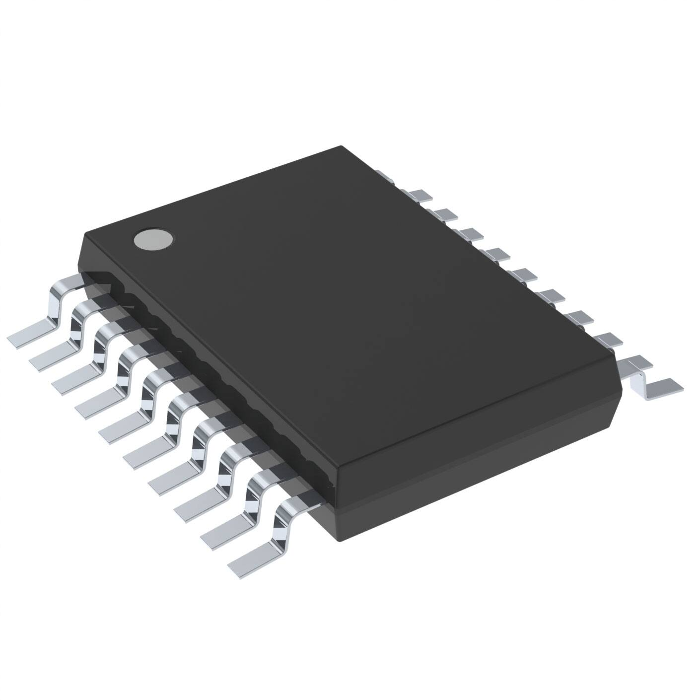
SN74BCT646 . . . DW OR NT PACKAGE
(TOP VIEW)
24
2
23
3
22
4
21
5
20
6
19
7
8
18
17
9
16
10
15
11
14
12
13
DIR
SAB
CLKAB
NC
VCC
CLKBA
SBA
1
VCC
CLKBA
SBA
OE
B1
B2
B3
B4
B5
B6
B7
B8
A1
A2
A3
NC
A4
A5
A6
5
1 28 27 26
25
6
24
7
23
8
22
9
21
10
20
4 3 2
19
11
12 13 14 15 16 17 18
A7
A8
GND
NC
B8
CLKAB
SAB
DIR
A1
A2
A3
A4
A5
A6
A7
A8
GND
SN54BCT646 . . . FK PACKAGE
(TOP VIEW)
OE
B1
B2
NC
B3
B4
B5
B7
B6
D
D
D Multiplexed Real-Time and Stored Data
D ESD Protection Exceeds JESD 22
Significantly Reduces ICCZ
Bus Transceivers/ Registers
Independent Registers and Enables for
A and B Buses
NC − No internal connection
description/ordering information
These devices consist of bus transceiver circuits, D-type flip-flops, and control circuitry arranged for multiplexed
transmission of data directly from the input bus or from the internal registers. Data on the A or B bus is clocked
into the registers on the low-to-high transition of the appropriate clock (CLKAB or CLKBA) input. Figure 1
illustrates the four fundamental bus-management functions that can be performed with the ’BCT646 devices.
Output-enable (OE) and direction-control (DIR) inputs are provided to control the transceiver functions. In the
transceiver mode, data present at the high-impedance port can be stored in either register or in both.
The select-control (SAB and SBA) inputs can multiplex stored and real-time (transparent mode) data. The
direction control (DIR) determines which bus will receive data when OE is low. In the isolation mode (OE high),
A data can be stored in one register and/or B data can be stored in the other register.
ORDERING INFORMATION
PDIP − NT
0°C
0
C to 70°C
70 C
−55°C to 125°C
†
ORDERABLE
PART NUMBER
PACKAGE†
TA
TOP-SIDE
MARKING
Tube
SN74BCT646NT
Tube
SN74BCT646DW
Tape and reel
SN74BCT646DWR
CDIP − JT
Tube
SNJ54BCT646JT
SNJ54BCT646JT
CFP − W
Tube
SNJ54BCT646W
SNJ54BCT646W
LCCC − FK
Tube
SNJ54BCT646FK
SNJ54BCT646FK
SOIC − DW
SN74BCT646NT
BCT646
Package drawings, standard packing quantities, thermal data, symbolization, and PCB design guidelines are
available at www.ti.com/sc/package.
Please be aware that an important notice concerning availability, standard warranty, and use in critical applications of
Texas Instruments semiconductor products and disclaimers thereto appears at the end of this data sheet.
Copyright © 2004, Texas Instruments Incorporated
PRODUCTION DATA information is current as of publication date.
Products conform to specifications per the terms of Texas Instruments
standard warranty. Production processing does not necessarily include
testing of all parameters.
On products compliant to MIL-PRF-38535, all parameters are tested
unless otherwise noted. On all other products, production
processing does not necessarily include testing of all parameters.
•
POST OFFICE BOX 655303 DALLAS, TEXAS 75265
POST OFFICE BOX 1443 HOUSTON, TEXAS 77251−1443
•
1
�SN54BCT646, SN74BCT646
OCTAL BUS TRANSCEIVERS AND REGISTERS
WITH 3-STATE OUTPUTS
SCBS037D − AUGUST 1989 − REVISED MAY 2004
description/ordering information(continued)
When an output function is disabled, the input function still is enabled and can be used to store and transmit
data. Only one of the two buses, A or B, can be driven at a time.
To ensure the high-impedance state during power up or power down, OE should be tied to VCC through a pullup
resistor; the minimum value of the resistor is determined by the current-sinking capability of the driver.
2
•
POST OFFICE BOX 655303 DALLAS, TEXAS 75265
POST OFFICE BOX 1443 HOUSTON, TEXAS 77251−1443
•
�SN54BCT646, SN74BCT646
OCTAL BUS TRANSCEIVERS AND REGISTERS
WITH 3-STATE OUTPUTS
21
OE
L
3
DIR
L
23
1
CLKAB CLKBA
X
X
21
OE
L
22
SBA
L
2
SAB
X
BUS B
BUS A
BUS A
BUS B
SCBS037D − AUGUST 1989 − REVISED MAY 2004
1
23
CLKAB CLKBA
X
↑
X
↑
↑
↑
2
SAB
X
X
X
2
SAB
L
22
SBA
X
BUS B
BUS A
BUS B
BUS A
3
DIR
X
X
X
23
CLKBA
X
REAL-TIME TRANSFER
BUS A TO BUS B
REAL-TIME TRANSFER
BUS B TO BUS A
21
OE
X
X
H
1
CLKAB
X
3
DIR
H
22
SBA
X
X
X
21
OE
L
L
STORAGE FROM
A, B, OR A AND B
3
DIR
L
H
1
CLKAB
X
H or L
23
CLKBA
H or L
X
2
SAB
X
H
22
SBA
H
X
TRANSFER STORED DATA
TO A AND/OR B
Pin numbers shown are for the DW, JT, NT, and W packages.
Figure 1. Bus-Management Functions
•
POST OFFICE BOX 655303 DALLAS, TEXAS 75265
POST OFFICE BOX 1443 HOUSTON, TEXAS 77251−1443
•
3
�SN54BCT646, SN74BCT646
OCTAL BUS TRANSCEIVERS AND REGISTERS
WITH 3-STATE OUTPUTS
SCBS037D − AUGUST 1989 − REVISED MAY 2004
FUNCTION TABLE
INPUTS
†
DATA I/O
OPERATION OR FUNCTION
OE
DIR
CLKAB
CLKBA
SAB
SBA
A1 THRU A8
B1 THRU B8
X
X
↑
X
X
X
Input
Unspecified†
Store A, B unspecified†
Input
Store B, A unspecified†
Store A and B data
X
X
X
↑
X
X
Unspecified†
H
X
↑
↑
X
X
Input
Input
H
X
H or L
H or L
X
X
Input disabled
Input disabled
Isolation, hold storage
L
L
X
X
X
L
Output
Input
Real-time B data to A bus
L
L
X
H or L
X
H
Output
Input
Stored B data to A bus
L
H
X
X
L
X
Input
Output
Real-time A data to B bus
L
H
H or L
X
H
X
Input
Output
Stored A data to B bus
The data output functions can be enabled or disabled by various signals at the OE and DIR inputs. Data input functions always are enabled, i.e.,
data at the bus pins is stored on every low-to-high transition of the clock inputs.
logic diagram (positive logic)
OE
DIR
CLKBA
SBA
CLKAB
SAB
21
3
23
22
1
2
One of Eight
Channels
1D
C1
A1
4
20
1D
C1
To Seven Other Channels
Pin numbers shown are for the DW, JT, NT, and W packages.
4
•
POST OFFICE BOX 655303 DALLAS, TEXAS 75265
POST OFFICE BOX 1443 HOUSTON, TEXAS 77251−1443
•
B1
�SN54BCT646, SN74BCT646
OCTAL BUS TRANSCEIVERS AND REGISTERS
WITH 3-STATE OUTPUTS
SCBS037D − AUGUST 1989 − REVISED MAY 2004
absolute maximum ratings over operating free-air temperature range (unless otherwise noted)†
Supply voltage range, VCC . . . . . . . . . . . . . . . . . . . . . . . . . . . . . . . . . . . . . . . . . . . . . . . . . . . . . . . . . . . −0.5 V to 7 V
Input voltage range: Control inputs (see Note 1) . . . . . . . . . . . . . . . . . . . . . . . . . . . . . . . . . . . . . . . . −0.5 V to 7 V
I/O ports (see Note 1) . . . . . . . . . . . . . . . . . . . . . . . . . . . . . . . . . . . . . . . . . . . −0.5 V to 5.5 V
Voltage range applied to any output in the disabled or power-off state, VO . . . . . . . . . . . . . . . . . −0.5 V to 7 V
Voltage range applied to any output in the high state, VO . . . . . . . . . . . . . . . . . . . . . . . . . . . . . . . . −0.5 V to VCC
Current into any output in the low state: SN54BCT646 . . . . . . . . . . . . . . . . . . . . . . . . . . . . . . . . . . . . . . . . 96 mA
SN74BCT646 . . . . . . . . . . . . . . . . . . . . . . . . . . . . . . . . . . . . . . . 128 mA
Package thermal impedance, θJA (see Note 2): DW package . . . . . . . . . . . . . . . . . . . . . . . . . . . . . . . . . 46°C/W
(see Note 3): NT package . . . . . . . . . . . . . . . . . . . . . . . . . . . . . . . . . 67°C/W
Storage temperature range, Tstg . . . . . . . . . . . . . . . . . . . . . . . . . . . . . . . . . . . . . . . . . . . . . . . . . . . . −65°C to 150°C
†
Stresses beyond those listed under “absolute maximum ratings” may cause permanent damage to the device. These are stress ratings only, and
functional operation of the device at these or any other conditions beyond those indicated under “recommended operating conditions” is not
implied. Exposure to absolute-maximum-rated conditions for extended periods may affect device reliability.
NOTES: 1. The input and output voltage ratings may be exceeded if the input and output current ratings are observed.
2. The package thermal impedance is calculated in accordance with JESD 51-7.
3. The package thermal impedance is calculated in accordance with JESD 51-3.
recommended operating conditions (see Note 4)
SN54BCT646
SN74BCT646
MIN
NOM
MAX
MIN
NOM
MAX
4.5
5
5.5
4.5
5
5.5
UNIT
VCC
Supply voltage
VIH
High-level input voltage
VIL
Low-level input voltage
0.8
0.8
V
IIK
Input clamp current
−18
−18
mA
IOH
High-level output current
−12
−15
mA
IOL
Low-level output current
48
64
mA
TA
Operating free-air temperature
70
°C
2
−55
2
125
0
V
V
NOTE 4: All unused control inputs of the device must be held at VCC or GND to ensure proper device operation. Refer to the TI application report,
Implications of Slow or Floating CMOS Inputs, literature number SCBA004.
•
POST OFFICE BOX 655303 DALLAS, TEXAS 75265
POST OFFICE BOX 1443 HOUSTON, TEXAS 77251−1443
•
5
�SN54BCT646, SN74BCT646
OCTAL BUS TRANSCEIVERS AND REGISTERS
WITH 3-STATE OUTPUTS
SCBS037D − AUGUST 1989 − REVISED MAY 2004
electrical characteristics over recommended operating free-air temperature range (unless
otherwise noted)
SN54BCT646
PARAMETER
VIK
TEST CONDITIONS
VCC = 4.5 V,
TYP†
2.4
3.3
2
3.2
II = −18 mA
IOH = −12 mA
VCC = 4.5 V
SN74BCT646
MAX
IOL = 48 mA
VCC = 4
4.5
5V
IIH‡
IIL‡
Control inputs
0.38
VCC = 5
5.5
5V
V,
VI = 5
5.5
5V
VCC = 5
5.5
5V
V,
VI = 2
2.7
7V
VCC = 5
5.5
5V
V,
VI = 0
0.5
5V
A or B port
Control inputs
IOS§
3.3
2
3.1
−100
MAX
−1.2
UNIT
V
0.55
0.42
A or B port
Control inputs
2.4
IOL = 64 mA
A or B port
II
TYP†
V
IOH = −15 mA
VOL
MIN
−1.2
IOH = − 3 mA
VOH
MIN
0.55
1
1
1
1
70
70
20
20
−0.7
−0.7
−0.7
−0.7
−225
−100
V
mA
μA
A
mA
VCC = 5.5 V,
VO = 0
ICCL
A or B port
VCC = 5.5 V,
VI = GND
42
−225
mA
67
mA
ICCH
A or B port
VCC = 5.5 V,
VI = 4.5 V
ICCZ
A or B port
VCC = 5.5 V,
VI = GND
5.6
9
mA
10
16
mA
Ci
Control inputs
VCC = 5 V,
VI = 2.5 V or 0.5 V
6
6
pF
Cio
A or B port
VCC = 5 V,
VO = 2.5 V or 0.5 V
12
14
pF
67
42
5.6
9
10
16
†
All typical values are at VCC = 5 V, TA = 25°C.
‡ For I/O ports, the parameters I and I include the off-state output current.
IH
IL
§ Not more than one output should be tested at a time, and the duration of the test should not exceed one second.
timing requirements over recommended ranges of supply voltage and operating free-air
temperature (unless otherwise noted)
VCC = 5 V,
TA = 25°C
MIN
MAX
SN54BCT646
MIN
MIN
Clock frequency
tw
Pulse duration, CLK high or low
6
6
6
ns
tsu
Setup time, A or B before CLKAB↑ or CLKBA↑
6
7
6
ns
th
Hold time, A or B after CLKAB↑ or CLKBA↑
0.5
0.5
0.5
ns
•
POST OFFICE BOX 655303 DALLAS, TEXAS 75265
POST OFFICE BOX 1443 HOUSTON, TEXAS 77251−1443
•
83
UNIT
MAX
fclock
6
83
MAX
SN7BCT646
83
MHz
�SN54BCT646, SN74BCT646
OCTAL BUS TRANSCEIVERS AND REGISTERS
WITH 3-STATE OUTPUTS
SCBS037D − AUGUST 1989 − REVISED MAY 2004
switching characteristics over recommended ranges of supply voltage and operating free-air
temperature, CL = 50 pF (unless otherwise noted) (see Figure 2)
PARAMETER
FROM
(INPUT)
VCC = 5 V,
TA = 25°C
TO
(OUTPUT)
MIN
fmax
tPLH
tPHL
tPLH
tPHL
tPLH
tPHL
tPLH
tPHL
tPZH
tPZL
tPHZ
tPLZ
tPZH
tPZL
tPHZ
tPLZ
†
TYP
SN54BCT646
MAX
83
CLKBA or CLKAB
A or B
A or B
B or A
SAB or SBA†
(with A or B high)
A or B
SAB or SBA†
(with A or B low)
A or B
OE
A or B
OE
A or B
DIR
A or B
DIR
A or B
MIN
MAX
83
SN74BCT646
MIN
UNIT
MAX
83
MHz
3.6
7
9.4
3.6
12.4
3.6
11.2
3.9
7
9.2
3.9
11.5
3.9
10.6
3.1
6
8.1
3.1
11.1
3.1
9.5
3.7
6.8
8.9
3.7
12.1
3.7
10.5
4.5
8.8
11.2
4.5
15.2
4.5
13.8
3.3
6
8.1
3.3
9.8
3.3
9.1
3.9
7.7
10.2
3.9
13.3
3.9
12
4.7
8.3
10.8
4.7
13.7
4.7
12.9
4
7.9
10.7
4
14
4
13.2
4.6
8.8
11.8
4.6
15.4
4.6
14.4
4
7.2
9.4
4
12
4
10.9
3.4
7
9.3
3.4
11.6
3.4
10.5
2.8
7.8
10.7
2.8
14
2.8
13.1
3.8
8.9
11.9
3.8
15.6
3.8
14.6
3.8
8.4
10.7
3.8
13.2
3.8
12.6
3.2
7.3
9.9
3.2
12.6
3.2
11.8
ns
ns
ns
ns
ns
ns
ns
ns
These parameters are measured with the internal output state of the storage register opposite that of the bus input.
•
POST OFFICE BOX 655303 DALLAS, TEXAS 75265
POST OFFICE BOX 1443 HOUSTON, TEXAS 77251−1443
•
7
�SN54BCT646, SN74BCT646
OCTAL BUS TRANSCEIVERS AND REGISTERS
WITH 3-STATE OUTPUTS
SCBS037D − AUGUST 1989 − REVISED MAY 2004
PARAMETER MEASUREMENT INFORMATION
7 V (tPZL, tPLZ, O.C.)
S1
Open
(all others)
From Output
Under Test
Test
Point
CL
(see Note A)
R1
From Output
Under Test
R1
Test
Point
CL
(see Note A)
R2
LOAD CIRCUIT FOR
TOTEM-POLE OUTPUTS
RL = R1 = R2
LOAD CIRCUIT FOR
3-STATE AND OPEN-COLLECTOR OUTPUTS
High-Level
Pulse
(see Note B)
3V
Timing Input
(see Note B)
3V
1.5 V
1.5 V
0V
1.5 V
tw
0V
Data Input
(see Note B)
3V
th
tsu
Low-Level
Pulse
3V
1.5 V
1.5 V
0V
1.5 V
1.5 V
VOLTAGE WAVEFORMS
PULSE DURATION
0V
VOLTAGE WAVEFORMS
SETUP AND HOLD TIMES
3V
Output
Control
(low-level enable)
3V
Input
(see Note B)
1.5 V
1.5 V
0V
In-Phase
Output
(see Note D)
VOH
1.5 V
Out-of-Phase
Output
(see Note D)
0V
1.5 V
3.5 V
VOL
tPHZ
tPLH
0.3 V
tPZH
VOH
1.5 V
tPLZ
1.5 V
Waveform 1
(see Notes C and D)
VOL
tPHL
1.5 V
tPZL
tPHL
tPLH
1.5 V
Waveform 2
(see Notes C and D)
1.5 V
VOL
VOH
1.5 V
0.3 V
0V
VOLTAGE WAVEFORMS
ENABLE AND DISABLE TIMES, 3-STATE OUTPUTS
VOLTAGE WAVEFORMS
PROPAGATION DELAY TIMES (see Note D)
NOTES: A. CL includes probe and jig capacitance.
B. All input pulses are supplied by generators having the following characteristics: PRR ≤ 10 MHz, tr = tf ≤ 2.5 ns, duty cycle = 50%.
C. Waveform 1 is for an output with internal conditions such that the output is low, except when disabled by the output control.
Waveform 2 is for an output with internal conditions such that the output is high, except when disabled by the output control.
D. The outputs are measured one at a time, with one transition per measurement.
E. When measuring propagation delay times of 3-state outputs, switch S1 is open.
F. All parameters and waveforms are not applicable to all devices.
Figure 2. Load Circuit and Voltage Waveforms
8
•
POST OFFICE BOX 655303 DALLAS, TEXAS 75265
POST OFFICE BOX 1443 HOUSTON, TEXAS 77251−1443
•
�PACKAGE OPTION ADDENDUM
www.ti.com
14-Oct-2022
PACKAGING INFORMATION
Orderable Device
Status
(1)
Package Type Package Pins Package
Drawing
Qty
Eco Plan
(2)
Lead finish/
Ball material
MSL Peak Temp
Op Temp (°C)
Device Marking
(3)
Samples
(4/5)
(6)
5962-9155501M3A
ACTIVE
LCCC
FK
28
1
Non-RoHS
& Green
SNPB
N / A for Pkg Type
-55 to 125
59629155501M3A
SNJ54BCT
646FK
5962-9155501MLA
ACTIVE
CDIP
JT
24
1
Non-RoHS
& Green
SNPB
N / A for Pkg Type
-55 to 125
5962-9155501ML
A
SNJ54BCT646JT
SN74BCT646DW
ACTIVE
SOIC
DW
24
25
RoHS & Green
NIPDAU
Level-1-260C-UNLIM
0 to 70
SNJ54BCT646FK
ACTIVE
LCCC
FK
28
1
Non-RoHS
& Green
SNPB
N / A for Pkg Type
-55 to 125
59629155501M3A
SNJ54BCT
646FK
SNJ54BCT646JT
ACTIVE
CDIP
JT
24
1
Non-RoHS
& Green
SNPB
N / A for Pkg Type
-55 to 125
5962-9155501ML
A
SNJ54BCT646JT
BCT646
(1)
The marketing status values are defined as follows:
ACTIVE: Product device recommended for new designs.
LIFEBUY: TI has announced that the device will be discontinued, and a lifetime-buy period is in effect.
NRND: Not recommended for new designs. Device is in production to support existing customers, but TI does not recommend using this part in a new design.
PREVIEW: Device has been announced but is not in production. Samples may or may not be available.
OBSOLETE: TI has discontinued the production of the device.
(2)
RoHS: TI defines "RoHS" to mean semiconductor products that are compliant with the current EU RoHS requirements for all 10 RoHS substances, including the requirement that RoHS substance
do not exceed 0.1% by weight in homogeneous materials. Where designed to be soldered at high temperatures, "RoHS" products are suitable for use in specified lead-free processes. TI may
reference these types of products as "Pb-Free".
RoHS Exempt: TI defines "RoHS Exempt" to mean products that contain lead but are compliant with EU RoHS pursuant to a specific EU RoHS exemption.
Green: TI defines "Green" to mean the content of Chlorine (Cl) and Bromine (Br) based flame retardants meet JS709B low halogen requirements of


 工商网监
湘ICP备2023018690号
工商网监
湘ICP备2023018690号
