Product
Folder
Sample &
Buy
Support &
Community
Tools &
Software
Technical
Documents
SN74CB3Q16244
SCDS168A – MAY 2004 – REVISED SEPTEMBER 2015
SN74CB3Q16244 16-Bit FET Bus Switch
2.5-V – 3.3-V Low-Voltage High-Bandwidth Bus Switch
1 Features
•
•
1
•
•
•
•
•
•
•
•
•
•
•
•
•
•
(1)
2 Applications
(1)
High-Bandwidth Data Path (Up to 500 MHz)
5-V Tolerant I/Os With Device Powered Up or
Powered Down
Low and Flat ON-State Resistance (ron)
Characteristics Over Operating Range
(ron= 5 Ω Typical)
Rail-to-Rail Switching on Data I/O Ports
– 0 to 5-V Switching With 3.3-V VCC
– 0 to 3.3-V Switching With 2.5-V VCC
Bidirectional Data Flow With Near-Zero
Propagation Delay
Low Input and Output Capacitance Minimizes
Loading and Signal Distortion
(Cio(OFF) = 4 pF Typical)
Fast Switching Frequency (fOE = 20 MHz
Maximum)
Data and Control Inputs Provide Undershoot
Clamp Diodes
Low Power Consumption (ICC = 1 mA Typical)
VCC Operating Range From 2.3 V to 3.6 V
Data I/Os Support 0 to 5-V Signaling Levels
(0.8 V, 1.2 V, 1.5 V, 1.8 V, 2.5 V, 3.3 V, 5 V)
Control Inputs Can Be Driven by TTL or
5-V and 3.3-V CMOS Outputs
Ioff Supports Partial-Power-Down Mode Operation
Latch-Up Performance Exceeds 100 mA
Per JESD 78, Class II
ESD Performance Tested Per JESD 22
– 2000-V Human Body Model
(A114-B, Class II)
– 1000-V Charged-Device Model (C101)
Supports Both Digital and Analog Applications
•
•
•
•
•
IP Phones: Wired and Wireless
Optical Modules
Optical Networking: Video Over Fiber and EPON
Private Branch Exchange (PBX)
WiMAX and Wireless Infrastructure Equipment
3 Description
The SN74CB3Q16244 device is a high-bandwidth
FET bus switch using a charge pump to elevate the
gate voltage of the pass transistor, providing a low
and flat ON-state resistance (ron). The low and flat
ON-state resistance allows for minimal propagation
delay and supports rail-to-rail switching on the data
input/output (I/O) ports. The SN74CB3Q16244 device
also features low data I/O capacitance to minimize
capacitive loading and signal distortion on the data
bus. Specifically designed to support high-bandwidth
applications, the SN74CB3Q16244 device provides
an optimized interface solution ideally suited for
broadband communications, networking, and dataintensive computing systems.
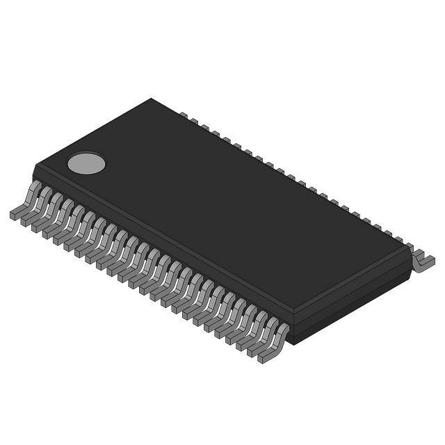
Device Information(1)
PACKAGE
BODY SIZE (NOM)
SN74CB3Q16244DGG TSSOP (48)
PART NUMBER
12.50 mm × 6.10 mm
SN74CB3Q16244DGV TVSOP (48)
9.70 mm × 4.40 mm
SN74CB3Q16244DL
15.88 mm × 7.49 mm
SSOP (48)
(1) For all available packages, see the orderable addendum at
the end of the data sheet.
Logic Diagram (Positive Logic)
47
1A1
2
SW
43
1A4
41
1B1
2A1
1B4
2A4
6
SW
37
1
For additional information regarding the performance
characteristics of the CB3Q family, refer to the TI application
report CBT-C, CB3T, and CB3Q Signal-Switch Families,
(SCDA008).
2B1
12
2B4
SW
48
1OE
2OE
36
3A1
13
SW
SW
25
30
3B1
4A1
3B4
4A4
17
32
3A4
3OE
8
SW
19
23
26
4OE
4B1
SW
SW
4B4
24
1
An IMPORTANT NOTICE at the end of this data sheet addresses availability, warranty, changes, use in safety-critical applications,
intellectual property matters and other important disclaimers. PRODUCTION DATA.
�SN74CB3Q16244
SCDS168A – MAY 2004 – REVISED SEPTEMBER 2015
www.ti.com
Table of Contents
1
2
3
4
5
6
7
8
9
Features ..................................................................
Applications ...........................................................
Description .............................................................
Revision History.....................................................
Description continued ...........................................
Pin Configuration and Functions .........................
Specifications.........................................................
1
1
1
2
3
4
5
7.1
7.2
7.3
7.4
7.5
7.6
7.7
5
5
5
5
6
6
7
Absolute Maximum Ratings .....................................
ESD Ratings..............................................................
Recommended Operating Conditions ......................
Thermal Information ..................................................
Electrical Characteristics ..........................................
Switching Characteristics ..........................................
Typical Characteristics ..............................................
Parameter Measurement Information .................. 8
Detailed Description .............................................. 9
9.1 Overview ................................................................... 9
9.2 Functional Block Diagram ......................................... 9
9.3 Feature Description................................................. 10
9.4 Device Functional Modes........................................ 10
10 Application and Implementation........................ 11
10.1 Application Information.......................................... 11
10.2 Typical Application ............................................... 11
11 Power Supply Recommendations ..................... 12
12 Layout................................................................... 13
12.1 Layout Guidelines ................................................. 13
12.2 Layout Example .................................................... 13
13 Device and Documentation Support ................. 14
13.1
13.2
13.3
13.4
13.5
Documentation Support ........................................
Community Resources..........................................
Trademarks ...........................................................
Electrostatic Discharge Caution ............................
Glossary ................................................................
14
14
14
14
14
14 Mechanical, Packaging, and Orderable
Information ........................................................... 14
4 Revision History
NOTE: Page numbers for previous revisions may differ from page numbers in the current version.
Changes from Revision A (March 2005) to Revision B
Page
•
Added Applications, Device Information table, Pin Configuration and Functions section, ESD Ratings table, Feature
Description section, Device Functional Modes, Application and Implementation section, Power Supply
Recommendations section, Layout section, Device and Documentation Support section, and Mechanical,
Packaging, and Orderable Information section ..................................................................................................................... 1
•
Removed Ordering Information table. ................................................................................................................................... 1
2
Submit Documentation Feedback
Copyright © 2004–2015, Texas Instruments Incorporated
Product Folder Links: SN74CB3Q16244
�SN74CB3Q16244
www.ti.com
SCDS168A – MAY 2004 – REVISED SEPTEMBER 2015
5 Description continued
The SN74CB3Q16244 device is organized as four 4-bit bus switches with separate output-enable (1OE, 2OE,
3OE, 4OE) inputs. It can be used as four 4-bit bus switches, two 8-bit bus switches, or one 16-bit bus switch.
When OE is low, the associated 4-bit bus switch is ON, and the A port is connected to the B port, allowing
bidirectional data flow between ports. When OE is high, the associated 4-bit bus switch is OFF, and a highimpedance state exists between the A and B ports.
This device is fully specified for partial-power-down applications using Ioff. The Ioff circuitry prevents damaging
current backflow through the device when it is powered down. The device has isolation during power off.
To ensure the high-impedance state during power up or power down, OE should be tied to VCC through a pullup
resistor; the minimum value of the resistor is determined by the current-sinking capability of the driver.
Submit Documentation Feedback
Copyright © 2004–2015, Texas Instruments Incorporated
Product Folder Links: SN74CB3Q16244
3
�SN74CB3Q16244
SCDS168A – MAY 2004 – REVISED SEPTEMBER 2015
www.ti.com
6 Pin Configuration and Functions
DGG, DGV, or DL Package
48-Pin TSSOP, TVSOP, or SSOP
Top View
1OE
1B1
1B2
GND
1B3
1B4
VCC
2B1
2B2
GND
2B3
2B4
3B1
3B2
GND
3B3
3B4
VCC
4B1
4B2
GND
4B3
4B4
4OE
1
48
2
47
3
46
4
45
5
44
6
43
7
42
8
41
9
40
10
39
11
38
12
37
13
36
14
35
15
34
16
33
17
32
18
31
19
30
20
29
21
28
22
27
23
26
24
25
2OE
1A1
1A2
GND
1A3
1A4
VCC
2A1
2A2
GND
2A3
2A4
3A1
3A2
GND
3A3
3A4
VCC
4A1
4A2
GND
4A3
4A4
3OE
Pin Functions
PIN
NAME
NO.
I/O
DESCRIPTION
1A1, 1A2
1A3, 1A4
47, 46
44, 43
I/O
Bidirectional signal to be switched
1B1, 1B2
1B3, 1B4
2, 3
5, 6
I/O
Bidirectional signal to be switched
1
I
2A1, 2A2
2A3, 2A4
41, 40
38, 37
I/O
Bidirectional signal to be switched
2B1, 2B2
2B3, 2B4
8, 9
11, 12
I/O
Bidirectional signal to be switched
48
I
3A1, 3A2
3A3, 3A4
36, 35
33, 32
I/O
Bidirectional signal to be switched
3B1, 3B2
3B3, 3B4
13, 14
16, 17
I/O
Bidirectional signal to be switched
25
I
4A1, 4A2
4A3, 4A4
30, 29
27, 26
I/O
Bidirectional signal to be switched
4B1, 4B2
4B3, 4B4
19, 20
22, 23
I/O
Bidirectional signal to be switched
4OE
24
I
VCC
7, 18, 31, 42
—
Power Supply
GND
4, 10, 15, 21
28, 34, 39, 45
—
Ground
1OE
2OE
3OE
4
Switch Output Enable to connect pins 1A1, 1A2, 1A3, 1A4 to 1B1, 1B2, 1B3, 1B4
(Active Low: L = ON, H = OFF)
Switch Output Enable to connect pins 2A1, 2A2, 2A3, 2A4 to 2B1, 2B2, 2B3, 2B4
(Active Low: L = ON, H = OFF)
Switch Output Enable to connect pins 3A1, 3A2, 3A3, 3A4 to 3B1, 3B2, 3B3, 3B4
(Active Low: L = ON, H = OFF)
Switch Output Enable to connect pins 4A1, 4A2, 4A3, 4A4 to 4B1, 4B2, 4B3, 4B4
(Active Low: L = ON, H = OFF)
Submit Documentation Feedback
Copyright © 2004–2015, Texas Instruments Incorporated
Product Folder Links: SN74CB3Q16244
�SN74CB3Q16244
www.ti.com
SCDS168A – MAY 2004 – REVISED SEPTEMBER 2015
7 Specifications
7.1 Absolute Maximum Ratings
over operating free-air temperature range (unless otherwise noted) (1)
MIN
MAX
UNIT
–0.5
4.6
V
VIN
Control input voltage
(2) (3)
–0.5
7
V
VI/O
Switch I/O voltage (2) (3) (4)
–0.5
7
V
IIK
Control input clamp current
VIN < 0
–50
mA
II/OK
I/O port clamp current
VI/O < 0
–50
mA
II/O
ON-state switch current (5)
±64
mA
Continuous current through VCC or GND
±100
mA
Supply voltage (2)
VCC
TJ
Junction temperature
Tstg
Storage temperature
(1)
(2)
(3)
(4)
(5)
150
–65
°C
150
Stresses beyond those listed under Absolute Maximum Ratings may cause permanent damage to the device. These are stress ratings
only, and functional operation of the device at these or any other conditions beyond those indicated under Recommended Operating
Conditions is not implied. Exposure to absolute-maximum-rated conditions for extended periods may affect device reliability.
All voltages are with respect to ground, unless otherwise specified.
The input and output voltage ratings may be exceeded if the input and output clamp-current ratings are observed.
VI and VO are used to denote specific conditions for VI/O.
II and IO are used to denote specific conditions for II/O.
7.2 ESD Ratings
VALUE
V(ESD)
(1)
(2)
Electrostatic discharge
Human body model (HBM), per ANSI/ESDA/JEDEC JS-001 (1)
+2000
Charged-device model (CDM), per JEDEC specification JESD22C101 (2)
+1000
UNIT
V
JEDEC document JEP155 states that 500-V HBM allows safe manufacturing with a standard ESD control process.
JEDEC document JEP157 states that 250-V CDM allows safe manufacturing with a standard ESD control process.
7.3 Recommended Operating Conditions
over operating free-air temperature range (unless otherwise noted) (1)
VCC
Supply voltage
VIH
High-level control input voltage
VIL
Low-level control input voltage
VI/O
Data input/output voltage
TA
Operating free-air temperature
(1)
MIN
MAX
UNIT
2.3
3.6
VCC = 2.3 V to 2.7 V
1.7
5.5
V
VCC = 2.7 V to 3.6 V
2
5.5
VCC = 2.3 V to 2.7 V
0
0.7
VCC = 2.7 V to 3.6 V
0
0.8
0
5.5
V
–40
85
°C
V
V
All unused control inputs of the device must be held at VCC or GND to ensure proper device operation. Refer to the TI application report,
Implications of Slow or Floating CMOS Inputs (SCBA004).
7.4 Thermal Information
SN74CB3Q16244
THERMAL METRIC (1)
RθJA
(1)
Junction-to-ambient thermal resistance
DGG (TSSOP)
DGV (TVSOP)
DL (SSOP)
48 PINS
48 PINS
48 PINS
70
58
63
UNIT
°C/W
For more information about traditional and new thermal metrics, see the Semiconductor and IC Package Thermal Metrics application
report, SPRA953.
Submit Documentation Feedback
Copyright © 2004–2015, Texas Instruments Incorporated
Product Folder Links: SN74CB3Q16244
5
�SN74CB3Q16244
SCDS168A – MAY 2004 – REVISED SEPTEMBER 2015
www.ti.com
7.5 Electrical Characteristics
over recommended operating free-air temperature range (unless otherwise noted) (1)
PARAMETER
VIK
MIN TYP (2)
TEST CONDITIONS
VCC = 3.6 V,
II = –18 mA
VCC = 3.6 V,
VIN = 0 to 5.5 V
IOZ (3)
VCC = 3.6 V,
VO = 0 to 5.5 V,
VI = 0,
Switch OFF,
VIN = VCC or GND
Ioff
VCC = 0,
VO = 0 to 5.5 V,
VI = 0
VCC = 3.6 V,
II/O = 0,
Switch ON or OFF,
VIN = VCC or GND
Other inputs at VCC or GND
IIN
Control inputs
ICC
ΔICC (4)
VCC = 3.6 V,
One input at 3 V,
Per control
input
VCC = 3.6 V,
A and B ports open,
Control input switching at 50% duty cycle
Control inputs
VCC = 3.3 V,
VIN = 5.5 V, 3.3 V, or 0
Cio(OFF)
VCC = 3.3 V,
Switch OFF,
VIN = VCC or GND,
Cio(ON)
VCC = 3.3 V,
ICCD
(5)
Cin
Control inputs
VCC = 2.3 V,
TYP at VCC = 2.5 V
ron (6)
VCC = 3 V
(1)
(2)
(3)
(4)
(5)
MAX
UNIT
–1.8
V
±1
µA
±1
µA
1
µA
2
mA
1
30
µA
mA/
MHz
0.15
0.25
3.5
5
pF
VI/O = 5.5 V, 3.3 V, or 0
4
6
pF
Switch ON,
VIN = VCC or GND,
VI/O = 5.5 V, 3.3 V, or 0
10
13
pF
VI = 0,
IO = 30 mA
6
8
VI = 1.7 V,
IO = –15 mA
5
10
VI = 0,
IO = 30 mA
6
8
VI = 2.4 V,
IO = –15 mA
5
9
Ω
VIN and IIN refer to control inputs. VI, VO, II, and IO refer to data pins.
All typical values are at VCC = 3.3 V (unless otherwise noted), TA = 25°C.
For I/O ports, the parameter IOZ includes the input leakage current.
This is the increase in supply current for each input that is at the specified TTL voltage level, rather than VCC or GND.
This parameter specifies the dynamic power-supply current associated with the operating frequency of a single control input
(see Figure 1).
Measured by the voltage drop between the A and B terminals at the indicated current through the switch. ON-state resistance is
determined by the lower of the voltages of the two (A or B) terminals.
(6)
7.6 Switching Characteristics
over recommended operating free-air temperature range (unless otherwise noted) (see Figure 2)
VCC = 2.5 V
± 0.2 V
VCC = 3.3 V
± 0.3 V
FROM
(INPUT)
TO
(OUTPUT)
fOE (1)
OE
A or B
10
20
MHz
tpd (2)
A or B
B or A
0.18
0.3
ns
ten
OE
A or B
1.5
8
1.5
7
ns
tdis
OE
A or B
1
8
1
7
ns
PARAMETER
(1)
(2)
6
MIN
MAX
MIN
UNIT
MAX
Maximum switching frequency for control input (VO > VCC, VI = 5 V, RL ≥ 1 MΩ, CL = 0)
The propagation delay is the calculated RC time constant of the typical ON-state resistance of the switch and the specified load
capacitance, when driven by an ideal voltage source (zero output impedance).
Submit Documentation Feedback
Copyright © 2004–2015, Texas Instruments Incorporated
Product Folder Links: SN74CB3Q16244
�SN74CB3Q16244
www.ti.com
SCDS168A – MAY 2004 – REVISED SEPTEMBER 2015
7.7 Typical Characteristics
12
VCC = 3.3 V
TA = 25°C
A and B Ports Open
10
ICC − mA
8
6
4
One OE Switching
2
0
0
2
4
6
8
10
12
14
16
18
20
OE Switching Frequency − MHz
Figure 1. Typical ICC vs OE Switching Frequency
Submit Documentation Feedback
Copyright © 2004–2015, Texas Instruments Incorporated
Product Folder Links: SN74CB3Q16244
7
�SN74CB3Q16244
SCDS168A – MAY 2004 – REVISED SEPTEMBER 2015
www.ti.com
8 Parameter Measurement Information
VCC
Input Generator
VIN
50 Ω
50 Ω
VG1
TEST CIRCUIT
DUT
2 × VCC
Input Generator
VI
S1
RL
VO
50 Ω
50 Ω
VG2
RL
CL
(see Note A)
TEST
VCC
S1
RL
VI
CL
tpd(s)
2.5 V ± 0.2 V
3.3 V ± 0.3 V
Open
Open
500 Ω
500 Ω
VCC or GND
VCC or GND
30 pF
50 pF
tPLZ/tPZL
2.5 V ± 0.2 V
3.3 V ± 0.3 V
2 × VCC
2 × VCC
500 Ω
500 Ω
GND
GND
30 pF
50 pF
0.15 V
0.3 V
tPHZ/tPZH
2.5 V ± 0.2 V
3.3 V ± 0.3 V
GND
GND
500 Ω
500 Ω
VCC
VCC
30 pF
50 pF
0.15 V
0.3 V
V∆
VCC
Output
Control
(VIN)
VCC/2
VCC
VCC/2
VCC/2
0V
tPLH
VOH
Output
VCC/2
Output
Waveform 1
S1 at 2 × VCC
(see Note B)
tPLZ
VCC
VCC/2
VCC/2
VOL
Output
Waveform 2
S1 at GND
(see Note B)
VOLTAGE WAVEFORMS
PROPAGATION DELAY TIMES (tpd(s))
VOL + V∆
VOL
tPZH
tPHL
VCC/2
0V
tPZL
Output
Control
(VIN)
Open
GND
tPHZ
VOH
VCC/2
VOH − V∆
0V
VOLTAGE WAVEFORMS
ENABLE AND DISABLE TIMES
NOTES: A. CL includes probe and jig capacitance.
B. Waveform 1 is for an output with internal conditions such that the output is low, except when disabled by the output control.
Waveform 2 is for an output with internal conditions such that the output is high, except when disabled by the output control.
C. All input pulses are supplied by generators having the following characteristics: PRR ≤ 10 MHz, ZO = 50 Ω, tr ≤ 2.5 ns, tf ≤ 2.5 ns.
D. The outputs are measured one at a time, with one transition per measurement.
E. tPLZ and tPHZ are the same as tdis.
F. tPZL and tPZH are the same as ten.
G. tPLH and tPHL are the same as tpd(s). The tpd propagation delay is the calculated RC time constant of the typical ON-state resistance
of the switch and the specified load capacitance, when driven by an ideal voltage source (zero output impedance).
H. All parameters and waveforms are not applicable to all devices.
Figure 2. Test Circuit and Voltage Waveforms
8
Submit Documentation Feedback
Copyright © 2004–2015, Texas Instruments Incorporated
Product Folder Links: SN74CB3Q16244
�SN74CB3Q16244
www.ti.com
SCDS168A – MAY 2004 – REVISED SEPTEMBER 2015
9 Detailed Description
9.1 Overview
The SN74CB3Q16244 is part of the CB3Q family of switches. The SN74CB3Q16244 is a 16-bit FET bus switch
in which 4 Output Enable pins each control a set of 4 switches totaling 16 switches.
B
A
VCC
Charge
Pump
EN(1)
(1)
EN is the internal enable signal applied to the switch.
Figure 3. Simplified Schematic, Each FET Switch (SW)
9.2 Functional Block Diagram
47
1A1
2
SW
2A1
1B4
2A4
6
43
1A4
41
1B1
SW
1
2B1
12
37
2B4
SW
48
1OE
2OE
36
3A1
13
SW
30
3B1
4A1
3B4
4A4
17
32
3A4
3OE
8
SW
SW
25
19
23
26
4OE
4B1
SW
SW
4B4
24
Figure 4. Logic Diagram (Positive Logic)
Submit Documentation Feedback
Copyright © 2004–2015, Texas Instruments Incorporated
Product Folder Links: SN74CB3Q16244
9
�SN74CB3Q16244
SCDS168A – MAY 2004 – REVISED SEPTEMBER 2015
www.ti.com
9.3 Feature Description
The SN74CB3Q16244 device has a high-bandwidth data path (up to 500 MHz) and has 5-V tolerant I/Os with the
device powered up or powered down. It also has low and flat ON-state resistance (ron) characteristics over
operating range (ron = 5 Ω Typical)
This device also has rail-to-rail switching on data I/O ports for 0 to 5-V switching with 3.3-V VCC and 0 to 3.3-V
switching with 2.5-V VCCas well as bidirectional data flow with near-zero propagation delay and low input and
output capacitance that minimizes loading and signal distortion (Cio(OFF) = 4 pF Typical)
The SN74CB3Q16244 also provides a fast switching frequency (fOE = 20 MHz Maximum) with data and control
inputs that provide undershoot clamp diodes as well as low power consumption (ICC = 1 mA Typical)
The VCC operating range is from 2.3 V to 3.6 V and the data I/Os support 0 to 5-V signal levels of (0.8-V, 1.2-V,
1.5-V, 1.8-V, 2.5-V, 3.3-V, 5-V)
The control inputs can be driven by TTL or 5-V and 3.3-V CMOS outputs, and Ioff supports partial-power-down
mode operation.
9.4 Device Functional Modes
Table 1 lists the functional modes of the SN74CB3Q16244.
Table 1. Function Table
(Each Multiplexer/Demultiplexer)
10
INPUT
INPUT/OUTPUT
OE
A
L
B
A port = B port
H
Z
Disconnect
Submit Documentation Feedback
FUNCTION
Copyright © 2004–2015, Texas Instruments Incorporated
Product Folder Links: SN74CB3Q16244
�SN74CB3Q16244
www.ti.com
SCDS168A – MAY 2004 – REVISED SEPTEMBER 2015
10 Application and Implementation
NOTE
Information in the following applications sections is not part of the TI component
specification, and TI does not warrant its accuracy or completeness. TI’s customers are
responsible for determining suitability of components for their purposes. Customers should
validate and test their design implementation to confirm system functionality.
10.1 Application Information
The SN74CB3Q16244 device can be used to control up to 16 bits with 4 channels simultaneously.
10.2 Typical Application
The application shown in Figure 5 is a 16-bit bus being controlled. The OE pins are used to control the chip from
the bus controller. This is a generic example and can apply to many situations. If an application requires fewer
than 16 bits, ensure that the A side is tied either high or low on unused channels.
1OE
1
ron
1A1
47
1A2
1A3
1B2
1B3
ron
1A4
43
2OE
6
1B4
8
2B1
48
ron
2A1
41
2A2
2A3
2B2
2B3
ron
2A4
Bus
Controller
1B1
2
37
2B4
12
16
16
3OE
Device
25
ron
3A1
36
3A2
3A3
3B2
3B3
ron
3A4
32
4OE
ron
30
4B1
19
4B2
4B3
4A2
4A3
ron
26
4, 10,
15, 21
28, 34,
39, 45
4B4
23
7
GND
3B4
17
24
4A1
4A4
3B1
13
18
31
42
VCC
0.022 �F
VCC
0.022 �F
VCC
0.022 �F
VCC
0.022 �F
Figure 5. Typical Application of the SN74CB3Q16244
Submit Documentation Feedback
Copyright © 2004–2015, Texas Instruments Incorporated
Product Folder Links: SN74CB3Q16244
11
�SN74CB3Q16244
SCDS168A – MAY 2004 – REVISED SEPTEMBER 2015
www.ti.com
Typical Application (continued)
10.2.1 Design Requirements
A 0.022-µF bypass capacitor should be placed between each VCC pin and GND. Each capacitor must be placed
as close as possible to the SN74CB3Q16244 device.
10.2.2 Detailed Design Procedure
1. Recommended input conditions:
– For specified high and low levels, see VIH and VIL in Recommended Operating Conditions
– Inputs and outputs are overvoltage tolerant, which allows them to go as high as 5.5 V at any valid VCC
2. Recommended output conditions:
– Load currents must not exceed ±64 mA per channel
3. Frequency selection criterion:
– Added trace resistance or capacitance can reduce maximum frequency capability; use layout practices as
directed in Layout
10.2.3 Application Curve
ron – ON-State Resistance – W
16
14
12
VCC = 3.3 V
TA = 25°C
IO = −15 mA
10
8
6
4
2
0
0.0
0.5
1.0
1.5
2.0
2.5
3.0
3.5
4.0
4.5
5.0
VI − V
Figure 6. Typical ron vs VI
11 Power Supply Recommendations
The power supply can be any voltage between the minimum and maximum supply voltage rating listed in the
Absolute Maximum Ratings table.
Each VCC terminal should have a good bypass capacitor to prevent power disturbance. For devices with a single
supply, a 0.1-μF bypass capacitor is recommended. If multiple pins are labeled VCC, then a 0.01-μF or 0.022-μF
capacitor is recommended for each VCC because the VCC pins are tied together internally. For devices with dualsupply pins operating at different voltages, for example VCC and VDD, a 0.1-µF bypass capacitor is recommended
for each supply pin. To reject different frequencies of noise, use multiple bypass capacitors in parallel. Capacitors
with values of 0.1 μF and 1 μF are commonly used in parallel. The bypass capacitor must be installed as close to
the power terminal as possible for best results.
12
Submit Documentation Feedback
Copyright © 2004–2015, Texas Instruments Incorporated
Product Folder Links: SN74CB3Q16244
�SN74CB3Q16244
www.ti.com
SCDS168A – MAY 2004 – REVISED SEPTEMBER 2015
12 Layout
12.1 Layout Guidelines
Reflections and matching are closely related to the loop antenna theory but are different enough to be discussed
separately from the theory. When a PCB trace turns a corner at a 90° angle, a reflection can occur. A reflection
occurs primarily because of the change of width of the trace. At the apex of the turn, the trace width increases to
1.414 times the width. This increase upsets the transmission-line characteristics, especially the distributed
capacitance and self-inductance of the trace, which results in the reflection. Not all PCB traces can be straight;
therefore, some traces must turn corners. Figure 7 shows progressively better techniques of rounding corners.
Only the last example (BEST) maintains constant trace width and minimizes reflections.
12.2 Layout Example
BETTER
BEST
2W
WORST
1W min.
W
Figure 7. Trace Example
Submit Documentation Feedback
Copyright © 2004–2015, Texas Instruments Incorporated
Product Folder Links: SN74CB3Q16244
13
�SN74CB3Q16244
SCDS168A – MAY 2004 – REVISED SEPTEMBER 2015
www.ti.com
13 Device and Documentation Support
13.1 Documentation Support
13.1.1 Related Documentation
For related documentation see the following:
• CBT-C, CB3T, and CB3Q Signal-Switch Families, SCDA008
• Implications of Slow or Floating CMOS Inputs, SCBA004
• Selecting the Right Texas Instruments Signal Switch, SZZA030
13.2 Community Resources
The following links connect to TI community resources. Linked contents are provided "AS IS" by the respective
contributors. They do not constitute TI specifications and do not necessarily reflect TI's views; see TI's Terms of
Use.
TI E2E™ Online Community TI's Engineer-to-Engineer (E2E) Community. Created to foster collaboration
among engineers. At e2e.ti.com, you can ask questions, share knowledge, explore ideas and help
solve problems with fellow engineers.
Design Support TI's Design Support Quickly find helpful E2E forums along with design support tools and
contact information for technical support.
13.3 Trademarks
E2E is a trademark of Texas Instruments.
All other trademarks are the property of their respective owners.
13.4 Electrostatic Discharge Caution
These devices have limited built-in ESD protection. The leads should be shorted together or the device placed in conductive foam
during storage or handling to prevent electrostatic damage to the MOS gates.
13.5 Glossary
SLYZ022 — TI Glossary.
This glossary lists and explains terms, acronyms, and definitions.
14 Mechanical, Packaging, and Orderable Information
The following pages include mechanical, packaging, and orderable information. This information is the most
current data available for the designated devices. This data is subject to change without notice and revision of
this document. For browser-based versions of this data sheet, refer to the left-hand navigation.
14
Submit Documentation Feedback
Copyright © 2004–2015, Texas Instruments Incorporated
Product Folder Links: SN74CB3Q16244
�PACKAGE OPTION ADDENDUM
www.ti.com
10-Dec-2020
PACKAGING INFORMATION
Orderable Device
Status
(1)
Package Type Package Pins Package
Drawing
Qty
Eco Plan
(2)
Lead finish/
Ball material
MSL Peak Temp
Op Temp (°C)
Device Marking
(3)
(4/5)
(6)
74CB3Q16244DGGRG4
ACTIVE
TSSOP
DGG
48
2000
RoHS & Green
NIPDAU
Level-1-260C-UNLIM
-40 to 85
CB3Q16244
SN74CB3Q16244DGGR
ACTIVE
TSSOP
DGG
48
2000
RoHS & Green
NIPDAU
Level-1-260C-UNLIM
-40 to 85
CB3Q16244
SN74CB3Q16244DGVR
ACTIVE
TVSOP
DGV
48
2000
RoHS & Green
NIPDAU
Level-1-260C-UNLIM
-40 to 85
BW244
SN74CB3Q16244DL
ACTIVE
SSOP
DL
48
25
RoHS & Green
NIPDAU
Level-1-260C-UNLIM
-40 to 85
CB3Q16244
SN74CB3Q16244DLR
ACTIVE
SSOP
DL
48
1000
RoHS & Green
NIPDAU
Level-1-260C-UNLIM
-40 to 85
CB3Q16244
(1)
The marketing status values are defined as follows:
ACTIVE: Product device recommended for new designs.
LIFEBUY: TI has announced that the device will be discontinued, and a lifetime-buy period is in effect.
NRND: Not recommended for new designs. Device is in production to support existing customers, but TI does not recommend using this part in a new design.
PREVIEW: Device has been announced but is not in production. Samples may or may not be available.
OBSOLETE: TI has discontinued the production of the device.
(2)
RoHS: TI defines "RoHS" to mean semiconductor products that are compliant with the current EU RoHS requirements for all 10 RoHS substances, including the requirement that RoHS substance
do not exceed 0.1% by weight in homogeneous materials. Where designed to be soldered at high temperatures, "RoHS" products are suitable for use in specified lead-free processes. TI may
reference these types of products as "Pb-Free".
RoHS Exempt: TI defines "RoHS Exempt" to mean products that contain lead but are compliant with EU RoHS pursuant to a specific EU RoHS exemption.
Green: TI defines "Green" to mean the content of Chlorine (Cl) and Bromine (Br) based flame retardants meet JS709B low halogen requirements of


 工商网监
湘ICP备2023018690号
工商网监
湘ICP备2023018690号
