��������� ��
�����
��
� ������ �
�
����������������������
���� ����
�� �������
SDFS064A − D2032, MARCH 1987 − REVISED OCTOBER 1993
•
•
•
•
SN54F253 . . . J PACKAGE
SN74F253 . . . D OR N PACKAGE
(TOP VIEW)
3-State Versions of SN54F153 and
SN74F153
Permits Multiplexing From N Lines to
One Line
Performs Parallel-to-Serial Conversion
Package Options Include Plastic
Small-Outline Packages, Ceramic Chip
Carriers, and Standard Plastic and Ceramic
300-mil DIPs
1G
B
1C3
1C2
1C1
1C0
1Y
GND
description
These data selectors/multiplexers contain
inverters and drivers to supply full binary decoding
data selection to the AND-OR gates. Separate
output-control inputs are provided for each of the
two 4-line sections.
1
16
2
15
3
14
4
13
5
12
6
11
7
10
8
9
VCC
2G
A
2C3
2C2
2C1
2C0
2Y
B
1G
NC
VCC
2G
SN54F253 . . . FK PACKAGE
(TOP VIEW)
The 3-state outputs can interface with and drive
data lines of bus-organized systems. With all but
one of the common outputs disabled (at a
high-impedance state), the low impedance of the
single enabled output will drive the bus line to a
high or low logic level. Each output has its own
strobe (G) inputs. The output is disabled when its
strobe is high.
4
3 2 1 20 19
18
5
17
6
16
7
15
8
14
9 10 11 12 13
A
2C3
NC
2C2
2C1
1Y
GND
NC
2Y
2C0
1C3
1C2
NC
1C1
1C0
The SN54F253 is characterized for operation over
the full military temperature range of − 55°C to
125°C. The SN74F253 is characterized for
operation from 0°C to 70°C.
NC − No internal connection
FUNCTION TABLE
INPUTS
SELECT
DATA
STROBE
G
OUTPUT
Y
Z
B
A
C0
C1
C2
C3
X
X
X
X
X
X
H
L
L
L
X
X
X
L
L
L
L
H
X
X
X
L
H
L
H
X
L
X
X
L
L
L
H
X
H
X
X
L
H
H
L
X
X
L
X
L
L
H
L
X
X
H
X
L
H
H
H
X
X
X
L
L
L
H
H
X
X
X
H
L
H
Select inputs A and B are common to both sections.
Copyright 1993, Texas Instruments Incorporated
���������� �
�
���!"#$%�!� �& '("")�% $& !� *(+,�'$%�!� -$%).
�"!-('%& '!��!"# %! &*)'���'$%�!�& *)" %/) %)"#& !� �)0$& ��&%"(#)�%&
&%$�-$"- 1$""$�%2. �"!-('%�!� *"!')&&��3 -!)& �!% �)')&&$"�,2 ��',(-)
%)&%��3 !� $,, *$"$#)%)"&.
• DALLAS, TEXAS 75265
• HOUSTON, TEXAS 77251−1443
POST OFFICE BOX 655303
POST OFFICE BOX 1443
2−1
���������� ��
�����
��
� ������ �
�
����������������������
���� ����
�� �������
SDFS064A − D2032, MARCH 1987 − REVISED OCTOBER 1993
logic symbol†
A
B
1G
1C0
1C1
1C2
1C3
2G
2C0
2C1
2C2
2C3
14
2
1
6
5
4
3
0
1
G 0
3
MUX
EN
0
7
1
2
3
15
10
9
11
12
13
† This symbol is in accordance with ANSI/IEEE Std 91-1984 and IEC Publication 617-12.
Pin numbers shown are for the D, J, and N packages.
2−2
1Y
•
POST OFFICE BOX 655303 DALLAS, TEXAS 75265
POST OFFICE BOX 1443 HOUSTON, TEXAS 77251−1443
•
2Y
���������� ��
�����
��
� ������ �
�
����������������������
���� ����
�� �������
SDFS064A − D2032, MARCH 1987 − REVISED OCTOBER 1993
logic diagram (positive logic)
1G
1C0
1C1
1
6
5
7
1Y
Data 1
1C2
1C3
B
4
3
2
Select
A
2C0
2C1
14
10
11
Data 2
9
2C2
12
2Y
13
2C3
2G
15
Pin numbers shown are for the D, J, and N packages.
•
POST OFFICE BOX 655303 DALLAS, TEXAS 75265
POST OFFICE BOX 1443 HOUSTON, TEXAS 77251−1443
•
2−3
���������� ��
�����
��
� ������ �
�
����������������������
���� ����
�� �������
SDFS064A − D2032, MARCH 1987 − REVISED OCTOBER 1993
absolute maximum ratings over operating free-air temperature range (unless otherwise noted)†
Supply voltage range, VCC . . . . . . . . . . . . . . . . . . . . . . . . . . . . . . . . . . . . . . . . . . . . . . . . . . . . . . . . . . −0.5 V to 7 V
Input voltage range (see Note 1) . . . . . . . . . . . . . . . . . . . . . . . . . . . . . . . . . . . . . . . . . . . . . . . . . . . . . −1.2 V to 7 V
Input current range . . . . . . . . . . . . . . . . . . . . . . . . . . . . . . . . . . . . . . . . . . . . . . . . . . . . . . . . . . . . . . −30 mA to 5 mA
Voltage range applied to any output in the disabled or power-off state . . . . . . . . . . . . . . . . . . . −0.5 V to 5.5 V
Voltage range applied to any output in the high state . . . . . . . . . . . . . . . . . . . . . . . . . . . . . . . . . . −0.5 V to VCC
Current into any output in the low state: SN54F253 . . . . . . . . . . . . . . . . . . . . . . . . . . . . . . . . . . . . . . . . . . . 40 mA
SN74F253 . . . . . . . . . . . . . . . . . . . . . . . . . . . . . . . . . . . . . . . . . . . 48 mA
Operating free-air temperature range: SN54F253 . . . . . . . . . . . . . . . . . . . . . . . . . . . . . . . . . . . −55°C to 125°C
SN74F253 . . . . . . . . . . . . . . . . . . . . . . . . . . . . . . . . . . . . . . 0°C to 70°C
Storage temperature range . . . . . . . . . . . . . . . . . . . . . . . . . . . . . . . . . . . . . . . . . . . . . . . . . . . . . . . . −65°C to 150°C
† Stresses beyond those listed under “absolute maximum ratings” may cause permanent damage to the device. These are stress ratings only and
functional operation of the device at these or any other conditions beyond those indicated under “recommended operating conditions” is not
implied. Exposure to absolute-maximum-rated conditions for extended periods may affect device reliability.
NOTE 1: The input voltage ratings may be exceeded provided the input current ratings are observed.
recommended operating conditions
SN54F253
SN74F253
MIN
NOM
MAX
MIN
NOM
MAX
4.5
5
5.5
4.5
5
5.5
UNIT
VCC
VIH
Supply voltage
VIL
IIK
Low-level input voltage
0.8
0.8
V
Input clamp current
−18
−18
mA
IOH
IOL
High-level output current
−3
−3
mA
Low-level output current
20
24
mA
TA
Operating free-air temperature
70
°C
2−4
High-level input voltage
2
−55
•
POST OFFICE BOX 655303 DALLAS, TEXAS 75265
POST OFFICE BOX 1443 HOUSTON, TEXAS 77251−1443
•
2
125
0
V
V
���������� ��
�����
��
� ������ �
�
����������������������
���� ����
�� �������
SDFS064A − D2032, MARCH 1987 − REVISED OCTOBER 1993
electrical characteristics over recommended operating free-air temperature range (unless
otherwise noted)
PARAMETER
VIK
VOH
VCC = 4.5 V,
VCC = 4.5 V
VCC = 4.75 V,
MIN
II = − 18 mA
IOH = − 1 mA
VOL
VCC = 4.5 V
IOZH
IOZL
VCC = 5.5 V,
VCC = 5.5 V,
VO = 2.7 V
VO = 0.5 V
II
IIH
VCC = 5.5 V,
VCC = 5.5 V,
IIL
IOS‡
VCC = 5.5 V,
VCC = 5.5 V,
SN74F253
TYP†
MAX
MIN
−1.2
IOH = − 3 mA
IOH = − 1 mA to − 3 mA
IOL = 20 mA
IOL = 24 mA
ICCH
ICCL
SN54F253
TYP†
MAX
TEST CONDITIONS
−1.2
2.5
3.4
2.5
3.4
2.4
3.3
2.4
3.3
V
V
2.7
0.3
0.5
0.35
0.5
V
50
50
µA
−50
−50
µA
VI = 7 V
VI = 2.7 V
0.1
0.1
mA
20
20
µA
VI = 0.5 V
VO = 0
− 0.6
− 0.6
mA
−150
mA
−60
−150
−60
Condition A
11.5
16
11.5
16
Condition B
16
23
16
23
ICCZ
Condition C
16
23
16
† All typical values are at VCC = 5 V, TA = 25°C.
‡ Not more than one output should be shorted at a time, and the duration of the short circuit should not exceed one second.
NOTE 2: ICC is measured with the outputs open under the following conditions:
A. Inputs A, B, 1C3, and 2C3 at 4.5 V, other inputs grounded
B. All inputs grounded
C. Inputs 1G and 2G at 4.5 V, other inputs grounded
23
VCC = 5.5 V,
See Note 2
UNIT
mA
switching characteristics (see Note 3)
PARAMETER
FROM
(INPUT)
VCC = 5 V,
CL = 50 pF,
R1 = 500 Ω,
R2 = 500 Ω,
TA = 25°C
TO
(OUTPUT)
VCC = 4.5 V to 5.5 V,
CL = 50 pF,
R1 = 500 Ω,
R2 = 500 Ω,
TA = MIN to MAX§
′F253
tPLH
tPHL
A or B
Any Y
tPLH
tPHL
Any C
Any Y
tPZH
tPZL
G
Any Y
tPHZ
tPLZ
G
Any Y
UNIT
SN54F253
SN74F253
MIN
TYP
MAX
MIN
MAX
MIN
MAX
3.7
8.1
11.5
2.7
15
3.7
13
2.2
6.1
9
1.7
11
2.2
10
2.2
5.1
7
1.7
9
2.2
8
1.7
4.1
6
1.7
8
1.7
7
2.2
5.6
8
1.7
10
2.2
9
2.2
5.6
8
1.7
10
2.2
9
1.2
3.3
5
1.2
6.5
1.2
6
1.2
4
6
1.2
8
1.2
7
ns
ns
ns
ns
§ For conditions shown as MIN or MAX, use the appropriate value specified under recommended operating conditions.
NOTE 3: Load circuit and waveforms are shown in Section 1.
•
POST OFFICE BOX 655303 DALLAS, TEXAS 75265
POST OFFICE BOX 1443 HOUSTON, TEXAS 77251−1443
•
2−5
�PACKAGE MATERIALS INFORMATION
www.ti.com
5-Jan-2022
TAPE AND REEL INFORMATION
*All dimensions are nominal
Device
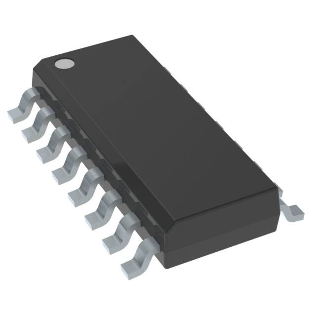
SN74F253DR
Package Package Pins
Type Drawing
SOIC
D
16
SPQ
Reel
Reel
A0
Diameter Width (mm)
(mm) W1 (mm)
2500
330.0
16.4
Pack Materials-Page 1
6.5
B0
(mm)
K0
(mm)
P1
(mm)
10.3
2.1
8.0
W
Pin1
(mm) Quadrant
16.0
Q1
�PACKAGE MATERIALS INFORMATION
www.ti.com
5-Jan-2022
*All dimensions are nominal
Device
Package Type
Package Drawing
Pins
SPQ
Length (mm)
Width (mm)
Height (mm)
SN74F253DR
SOIC
D
16
2500
340.5
336.1
32.0
Pack Materials-Page 2
�PACKAGE MATERIALS INFORMATION
www.ti.com
5-Jan-2022
TUBE
*All dimensions are nominal
Device
Package Name
Package Type
Pins
SPQ
L (mm)
SN74F253D
D
SOIC
16
40
507
SN74F253N
N
PDIP
16
25
506
SN74F253N
N
PDIP
16
25
506
13.97
Pack Materials-Page 3
W (mm)
T (µm)
B (mm)
8
3940
4.32
13.97
11230
4.32
11230
4.32
�IMPORTANT NOTICE AND DISCLAIMER
TI PROVIDES TECHNICAL AND RELIABILITY DATA (INCLUDING DATA SHEETS), DESIGN RESOURCES (INCLUDING REFERENCE
DESIGNS), APPLICATION OR OTHER DESIGN ADVICE, WEB TOOLS, SAFETY INFORMATION, AND OTHER RESOURCES “AS IS”
AND WITH ALL FAULTS, AND DISCLAIMS ALL WARRANTIES, EXPRESS AND IMPLIED, INCLUDING WITHOUT LIMITATION ANY
IMPLIED WARRANTIES OF MERCHANTABILITY, FITNESS FOR A PARTICULAR PURPOSE OR NON-INFRINGEMENT OF THIRD
PARTY INTELLECTUAL PROPERTY RIGHTS.
These resources are intended for skilled developers designing with TI products. You are solely responsible for (1) selecting the appropriate
TI products for your application, (2) designing, validating and testing your application, and (3) ensuring your application meets applicable
standards, and any other safety, security, regulatory or other requirements.
These resources are subject to change without notice. TI grants you permission to use these resources only for development of an
application that uses the TI products described in the resource. Other reproduction and display of these resources is prohibited. No license
is granted to any other TI intellectual property right or to any third party intellectual property right. TI disclaims responsibility for, and you
will fully indemnify TI and its representatives against, any claims, damages, costs, losses, and liabilities arising out of your use of these
resources.
TI’s products are provided subject to TI’s Terms of Sale or other applicable terms available either on ti.com or provided in conjunction with
such TI products. TI’s provision of these resources does not expand or otherwise alter TI’s applicable warranties or warranty disclaimers for
TI products.
TI objects to and rejects any additional or different terms you may have proposed. IMPORTANT NOTICE
Mailing Address: Texas Instruments, Post Office Box 655303, Dallas, Texas 75265
Copyright © 2022, Texas Instruments Incorporated
�


 工商网监
湘ICP备2023018690号
工商网监
湘ICP备2023018690号
