��������� �� �����
��
� ��
������ ��
���������� ���
�����
�
�� ������� ��������
�
The SN54F299 is obsolete and no
longer supplied.
SDFS071B − MARCH 1987 − REVISED APRIL 2004
D Four Modes of Operation:
D
D
D
D
D
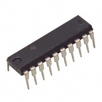
SN54F299 . . . J PACKAGE
SN74F299 . . . DW, N, OR NS PACKAGE
(TOP VIEW)
− Hold (Store)
− Shift Right
− Shift Left
− Load Data
Operates With Outputs Enabled or at High
Impedance
3-State Outputs Drive Bus Lines Directly
Can Be Cascaded for N-Bit Word Lengths
Direct Overriding Clear
Applications:
− Stacked or Pushdown Registers
− Buffer Storage
− Accumulator Registers
S0
OE1
OE2
G/QG
E/QE
C/QC
A/QA
QA′
CLR
GND
1
20
2
19
3
18
4
17
5
16
6
15
7
14
8
13
9
12
10
11
VCC
S1
SL
QH′
H/QH
F/QF
D/QD
B/QB
CLK
SR
SN54F299 . . . FK PACKAGE
(TOP VIEW)
OE2
OE1
S0
VCC
S1
description/ordering information
These 8-bit universal shift /storage registers
feature multiplexed I/O ports to achieve full 8-bit
data handling in a single 20-pin package. Two
function-select (S0, S1) inputs and two
output-enable (OE1, OE2) inputs can be used to
choose the modes of operation listed in the
function table.
G/QG
E/QE
C/QC
A/QA
QA′
4
3 2 1 20 19
18
5
17
6
16
7
15
8
14
SL
QH′
H/QH
F/QF
D/QD
CLR
GND
SR
CLK
B/QB
9 10 11 12 13
Synchronous parallel loading is accomplished by
taking both S0 and S1 high. This places the
3-state outputs in a high-impedance state and
permits data that is applied on the I/O ports to
be clocked into the register. Reading out of the register can be accomplished while the outputs are enabled in
any mode. Clearing occurs when the clear (CLR) input is low. Taking either OE1 or OE2 high disables the outputs
but has no effect on clearing, shifting, or storage of data.
ORDERING INFORMATION
PDIP − N
0°C to 70°C
ORDERABLE
PART NUMBER
PACKAGE†
TA
SOIC − DW
Tube of 20
SN74F299N
Tube of 25
SN74F299DW
Reel of 2000
SN74F299DWR
TOP-SIDE
MARKING
SN74F299N
F299
SOP − NS
Reel of 2000
SN74F299NSR
74F299
† Package drawings, standard packing quantities, thermal data, symbolization, and PCB design guidelines are
available at www.ti.com/sc/package.
Please be aware that an important notice concerning availability, standard warranty, and use in critical applications of
Texas Instruments semiconductor products and disclaimers thereto appears at the end of this data sheet.
Copyright 2004, Texas Instruments Incorporated
�������
�� ���� �!"#$%&'�#! �( )*$$+!' &( #" ,*-.�)&'�#! /&'+0
�$#/*)'( )#!"#$% '# (,+)�"�)&'�#!( ,+$ '1+ '+$%( #" �+2&(
!('$*%+!'(
('&!/&$/ 3&$$&!'40 �$#/*)'�#! ,$#)+((�!5 /#+( !#' !+)+((&$�.4 �!).*/+
'+('�!5 #" &.. ,&$&%+'+$(0
POST OFFICE BOX 655303
• DALLAS, TEXAS 75265
1
���������� �� �����
��
� ��
������ ��
���������� ���
�����
�
�� ������� ��������
�
The SN54F299 is obsolete and no
longer supplied.
SDFS071B − MARCH 1987 − REVISED APRIL 2004
FUNCTION TABLE
INPUTS
MODE
OE2†
I/O PORTS
OUTPUTS
CLR
S1
S0
OE1†
CLK
SL
SR
A/QA
B/QB
C/QC
D/QD
QA′
QH′
Clear
L
X
H
L
L
X
L
L
X
X
X
X
X
X
X
X
X
X
L
L
X
L
L
X
L
L
X
L
L
X
F/QF
L
L
X
H/QH
X
L
H
E/QE
L
L
X
G/QG
L
L
L
L
L
X
L
L
X
L
L
L
L
L
L
Hold
H
H
L
X
L
X
L
L
L
L
X
L
X
X
X
X
QA0
QA0
QB0
QB0
QC0
QC0
QD0
QD0
QE0
QE0
QF0
QF0
QG0
QG0
QH0
QH0
QA0
QA0
QH0
QH0
Shift
Right
H
H
L
L
H
H
L
L
L
L
↑
↑
X
X
H
L
H
L
QAn
QAn
QBn
QBn
QCn
QCn
QDn
QDn
QEn
QEn
QFn
QFn
QGn
QGn
H
L
QGn
QGn
Shift
Left
H
H
H
H
L
L
L
L
L
L
↑
↑
H
L
X
X
QBn
QBn
QCn
QCn
QDn
QDn
QEn
QEn
QFn
QFn
QGn
QGn
QHn
QHn
H
L
QBn
QBn
H
L
Load
H
H
H
X
X
↑
X
X
a
b
c
d
e
f
g
h
a
h
NOTE: a . . . h = the level of the steady-state input at inputs A through H, respectively. This data is loaded into the flip-flops while the flip-flop
outputs are isolated from the I/O terminals.
† When one or both output-enable inputs are high, the eight I/O terminals are disabled to the high-impedance state; however, sequential operation
or clearing of the register is not affected.
logic diagram (positive logic)
S0
S1
SR
(shift right
serial input)
CLK
1
19
18
11
Six
Identical
Channels
Not
Shown‡
12
1D
1D
C1
C1
R
QA′
CLR
OE1
OE2
R
8
17
9
2
3
7
16
A /QA
H /QH
‡ I/O ports not shown: B/QB (13), C/QC (6), D/QD (14), E/QE (5), F/QF (15), and G/QG (4).
2
SL
(shift left
serial input)
POST OFFICE BOX 655303
• DALLAS, TEXAS 75265
QH′
��
The SN54F299 is obsolete and no
longer supplied.
��������� �� �����
��
� ��
������ ��
���������� ���
�����
�
�� ������� ��������
SDFS071B − MARCH 1987 − REVISED APRIL 2004
absolute maximum ratings over operating free-air temperature range (unless otherwise noted)†
Supply voltage range, VCC . . . . . . . . . . . . . . . . . . . . . . . . . . . . . . . . . . . . . . . . . . . . . . . . . . . . . . . . . . −0.5 V to 7 V
Input voltage range, VI (see Note 1) . . . . . . . . . . . . . . . . . . . . . . . . . . . . . . . . . . . . . . . . . . . . . . . . . . −1.2 V to 7 V
Input current range . . . . . . . . . . . . . . . . . . . . . . . . . . . . . . . . . . . . . . . . . . . . . . . . . . . . . . . . . . . . . . . −30 mA to 5 mA
Voltage range applied to any output in the disabled or power-off state . . . . . . . . . . . . . . . . . . . . −0.5 V to 5.5 V
Voltage range applied to any output in the high state . . . . . . . . . . . . . . . . . . . . . . . . . . . . . . . . . . −0.5 V to VCC
Current into any output in the low state: QA′ or QH′ . . . . . . . . . . . . . . . . . . . . . . . . . . . . . . . . . . . . . . . . . . 40 mA
SN54F299 (QA thru QH) . . . . . . . . . . . . . . . . . . . . . . . . . . . . . . 40 mA
SN74F299 (QA thru QH) . . . . . . . . . . . . . . . . . . . . . . . . . . . . . . 48 mA
Package thermal impedance, θJA (see Note 2): DW package . . . . . . . . . . . . . . . . . . . . . . . . . . . . . . . . . 58°C/W
N package . . . . . . . . . . . . . . . . . . . . . . . . . . . . . . . . . . . 69°C/W
NS package . . . . . . . . . . . . . . . . . . . . . . . . . . . . . . . . . 60°C/W
Storage temperature range, Tstg . . . . . . . . . . . . . . . . . . . . . . . . . . . . . . . . . . . . . . . . . . . . . . . . . . . −65°C to 150°C
† Stresses beyond those listed under “absolute maximum ratings” may cause permanent damage to the device. These are stress ratings only, and
functional operation of the device at these or any other conditions beyond those indicated under “recommended operating conditions” is not
implied. Exposure to absolute-maximum-rated conditions for extended periods may affect device reliability.
NOTES: 1. The input voltage ratings may be exceeded provided the input current ratings are observed.
2. The package thermal impedance is calculated in accordance with JESD 51-7.
recommended operating conditions (see Note 3)
SN54F299
SN74F299
MIN
NOM
MAX
MIN
NOM
MAX
4.5
5
5.5
4.5
5
5.5
UNIT
VCC
VIH
Supply voltage
VIL
IIK
Low-level input voltage
0.8
0.8
V
Input clamp current
−18
−18
mA
−1
High-level output current
QA′ or QH′
−1
IOH
QA thru QH
−3
−3
20
Low-level output current
QA′ or QH′
20
IOL
QA thru QH
20
24
High-level input voltage
2
2
V
V
mA
mA
TA
Operating free-air temperature
−55
125
0
70
°C
NOTE 3: All unused inputs of the device must be held at VCC or GND to ensure proper device operation. Refer to the TI application report,
Implications of Slow or Floating CMOS Inputs, literature number SCBA004.
POST OFFICE BOX 655303
• DALLAS, TEXAS 75265
3
���������� �� �����
��
� ��
������ ��
���������� ���
�����
�
�� ������� ��������
�
The SN54F299 is obsolete and no
longer supplied.
SDFS071B − MARCH 1987 − REVISED APRIL 2004
electrical characteristics over recommended operating free-air temperature range (unless
otherwise noted)
PARAMETER
VIK
VCC = 4.5 V,
QA thru QH
Any output
VCC = 4.75 V,
QA thru QH
IIH‡
IIL‡
3.4
2.5
3.4
2.5
3.4
2.5
3.4
2.4
3.3
2.4
3.3
VCC = 5.5 V
VI = 5.5 V
VI = 7 V
VCC = 5.5 V,
VI = 2.7 V
0.3
0.5
0.3
0.5
0.3
0.5
0.35
0.5
V
1
1
0.1
70
70
20
20
A thru H
−0.65
−0.65
S0 or S1
−1.2
−1.2
−0.6
−0.6
A thru H
Any other
VCC = 5.5 V,
V
V
0.1
Any other
UNIT
2.7
IOL = 20 mA
IOL = 24 mA
A thru H
II
−1.2
2.5
IOH = − 1 mA to − 3 mA
IOL = 20 mA
VCC = 4.5 V
SN74F299
TYP†
MAX
MIN
−1.2
IOH = − 1 mA
IOH = − 3 mA
VCC = 4.5 V
QA′ or QH′
VOL
MIN
II = − 18 mA
IOH = − 1 mA
QA′ or QH′
VOH
SN54F299
TYP†
MAX
TEST CONDITIONS
VI = 0.5 V
Any other
IOS§
VCC = 5.5 V,
VO = 0
−60
−150
−60
ICC
VCC = 5.5 V,
See Note 4
68
95
68
† All typical values are at VCC = 5 V, TA = 25°C.
‡ For I/O ports (QA thru QH), the parameters IIH and IIL include the off-state output current.
§ Not more than one output should be shorted at a time, and the duration of the short circuit should not exceed one second.
NOTE 4: ICC is measured with OE1, OE2, and CLK at 4.5 V.
mA
µA
A
mA
−150
mA
95
mA
timing requirements over recommended ranges of supply voltage and operating free-air
temperature (unless otherwise noted)
VCC = 5 V,
TA = 25°C
SN54F299
SN74F299
MIN
MIN
′F299
MIN
fclock
tw
tsu
th
Clock frequency
Pulse duration
Setup time before
CLK↑
Inactive-state setup
time before CLK↑¶
Hold time after CLK↑
70
MAX
65
7
8
7
CLR low
7
8
7
S0 or S1
High or low
8.5
9.5
8.5
A/QA thru H/QH, SR, or SL
High or low
5.5
6.5
5.5
CLR
High
7
13
7
S0 or S1
High or low
0
0
0
A /QA thru H /QH, SR, or SL
High or low
2
2
2
POST OFFICE BOX 655303
• DALLAS, TEXAS 75265
MAX
70
CLK high or low
¶ Inactive-state setup time also is referred to as recovery time.
4
MAX
UNIT
MHz
ns
ns
ns
���������� �� �����
��
� ��
������ ��
���������� ���
�����
�
�� ������� ��������
�
The SN54F299 is obsolete and no
longer supplied.
SDFS071B − MARCH 1987 − REVISED APRIL 2004
switching characteristics (see Figure 1)
PARAMETER
FROM
(INPUT)
TO
(OUTPUT)
VCC = 5 V,
CL = 50 pF,
RL = 500 Ω,
TA = 25°C
VCC = 4.5 V to 5.5 V,
CL = 50 pF,
RL = 500 Ω,
TA = MIN to MAX†
′F299
fmax
tPLH
tPHL
tPLH
tPHL
CLK
QA
A′ or QH
H′
CLK
QA thru QH
MAX
UNIT
SN54F299
SN74F299
MIN
MIN
MIN
TYP
70
100
MAX
3.2
6.6
9
2.7
10.5
3.2
10
2.7
6.1
8.5
2.2
10
2.7
9.5
3.2
6.6
9
2.7
11
3.2
10
4.2
8.1
11
3.7
12.5
4.2
12
65
MAX
70
MHz
QA′ or QH′
3.7
7.1
9.5
3.2
11.5
3.7
10.5
QA thru QH
5.7
10.6
14
5
15.5
5.7
15
2.7
5.6
8
2.2
10.5
2.7
9
3.2
6.6
10
2.7
12
3.2
11
1.7
4.1
6
1.7
9
1.7
7
1.2
3.6
5.5
1.2
7.5
1.2
6.5
tPHL
CLR
tPZH
tPZL
OE1 or OE2
QA thru QH
tPHZ
tPLZ
OE1 or OE2
QA thru QH
ns
ns
ns
ns
ns
† For conditions shown as MIN or MAX, use the appropriate value specified under recommended operating conditions.
POST OFFICE BOX 655303
• DALLAS, TEXAS 75265
5
���������� �� �����
��
� ��
������ ��
���������� ���
�����
�
�� ������� ��������
�
The SN54F299 is obsolete and no
longer supplied.
SDFS071B − MARCH 1987 − REVISED APRIL 2004
PARAMETER MEASUREMENT INFORMATION
7V
From Output
Under Test
CL
(see Note A)
500 Ω S1
From Output
Under Test
Test
Point
CL
(see Note A)
500 Ω
Open
500 Ω
TEST
S1
tPLH/tPHL
tPLZ/tPZL
tPHZ/tPZH
Open
7V
Open
7V
Open Collector
LOAD CIRCUIT FOR
3-STATE AND OPEN-DRAIN OUTPUTS
LOAD CIRCUIT FOR
TOTEM-POLE OUTPUTS
3V
Timing Input
1.5 V
0V
tw
tsu
3V
1.5 V
Input
1.5 V
th
3V
1.5 V
1.5 V
Data Input
0V
1.5 V
VOLTAGE WAVEFORMS
SETUP AND HOLD TIMES
3V
1.5 V
Input
1.5 V
0V
tPLH
tPHL
1.5 V
1.5 V
VOL
tPHL
1.5 V
VOH
1.5 V
VOL
Output
Waveform 2
S1 at GND
(see Note B)
1.5 V
0V
Output
Waveform 1
S1 at 7 V
(see Note B)
tPLH
1.5 V
3V
Output
Control
tPZL
VOH
In-Phase
Output
Out-of-Phase
Output
0V
VOLTAGE WAVEFORMS
PULSE DURATION
tPLZ
1.5 V
tPZH
VOLTAGE WAVEFORMS
PROPAGATION DELAY TIMES
INVERTING AND NONINVERTING OUTPUTS
≈3.5 V
VOL + 0.3 V
VOL
tPHZ
1.5 V
VOH − 0.3 V
VOH
≈0 V
VOLTAGE WAVEFORMS
ENABLE AND DISABLE TIMES
LOW- AND HIGH-LEVEL ENABLING
NOTES: A. CL includes probe and jig capacitance.
B. Waveform 1 is for an output with internal conditions such that the output is low, except when disabled by the output control.
Waveform 2 is for an output with internal conditions such that the output is high, except when disabled by the output control.
C. All input pulses are supplied by generators having the following characteristics: PRR ≤ 1 MHz, ZO = 50 Ω, tr ≤ 2.5 ns, tf ≤ 2.5 ns,
duty cycle = 50%.
D. The outputs are measured one at a time, with one input transition per measurement.
Figure 1. Load Circuit and Voltage Waveforms
6
POST OFFICE BOX 655303
• DALLAS, TEXAS 75265
�PACKAGE OPTION ADDENDUM
www.ti.com
10-Dec-2020
PACKAGING INFORMATION
Orderable Device
Status
(1)
Package Type Package Pins Package
Drawing
Qty
Eco Plan
(2)
Lead finish/
Ball material
MSL Peak Temp
Op Temp (°C)
Device Marking
(3)
(4/5)
(6)
SN74F299DW
ACTIVE
SOIC
DW
20
25
RoHS & Green
NIPDAU
Level-1-260C-UNLIM
0 to 70
F299
SN74F299DWR
ACTIVE
SOIC
DW
20
2000
RoHS & Green
NIPDAU
Level-1-260C-UNLIM
0 to 70
F299
SN74F299N
ACTIVE
PDIP
N
20
20
RoHS &
Non-Green
NIPDAU
N / A for Pkg Type
0 to 70
SN74F299N
(1)
The marketing status values are defined as follows:
ACTIVE: Product device recommended for new designs.
LIFEBUY: TI has announced that the device will be discontinued, and a lifetime-buy period is in effect.
NRND: Not recommended for new designs. Device is in production to support existing customers, but TI does not recommend using this part in a new design.
PREVIEW: Device has been announced but is not in production. Samples may or may not be available.
OBSOLETE: TI has discontinued the production of the device.
(2)
RoHS: TI defines "RoHS" to mean semiconductor products that are compliant with the current EU RoHS requirements for all 10 RoHS substances, including the requirement that RoHS substance
do not exceed 0.1% by weight in homogeneous materials. Where designed to be soldered at high temperatures, "RoHS" products are suitable for use in specified lead-free processes. TI may
reference these types of products as "Pb-Free".
RoHS Exempt: TI defines "RoHS Exempt" to mean products that contain lead but are compliant with EU RoHS pursuant to a specific EU RoHS exemption.
Green: TI defines "Green" to mean the content of Chlorine (Cl) and Bromine (Br) based flame retardants meet JS709B low halogen requirements of