�������� ��
����
��
������ ������� ����������
�� �������
���� �������������� �������
SDFS013A − MARCH 1987 − REVISED OCTOBER 1993
•
SN54F38 . . . J PACKAGE
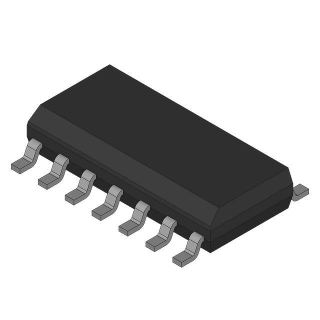
SN74F38 . . . D OR N PACKAGE
(TOP VIEW)
Package Options Include Plastic
Small-Outline Packages, Ceramic Chip
Carriers, and Standard Plastic and Ceramic
300-mil DIPs
1A
1B
1Y
2A
2B
2Y
GND
description
These devices contain four independent 2-input
NAND buffer gates with open-collector outputs.
They perform the Boolean functions Y = A • B or
Y = A + B in positive logic.
The open-collector outputs require pullup
resistors to perform correctly. They may be
connected to other open-collector outputs to
implement active-low wired-OR or active-high
wired-AND functions. Open-collector devices are
often used to generate higher VOH levels.
OUTPUT
Y
H
H
L
L
X
H
X
L
H
1B
2A
2B
3A
3B
4A
4B
1
12
4
11
5
10
6
9
7
8
4
3 2 1 20 19
18
5
17
6
16
7
15
8
14
9 10 11 12 13
4A
NC
4Y
NC
3B
NC − No internal connection
logic symbol†
1A
3
VCC
4B
4A
4Y
3B
3A
3Y
2Y
GND
NC
3Y
3A
B
13
1B
1A
NC
VCC
4B
1Y
NC
2A
NC
2B
FUNCTION TABLE
(each gate)
INPUTS
14
2
SN54F38 . . . FK PACKAGE
(TOP VIEW)
The SN54F38 is characterized for operation over
the full military temperature range of − 55°C to
125°C. The SN74F38 is characterized for
operation from 0°C to 70°C.
A
1
logic diagram (positive logic)
3
&
2
1A
1Y
1B
4
6
5
2A
2Y
2B
9
8
10
3A
3Y
3B
12
11
13
4Y
4A
4B
1
2
3
1Y
4
5
6
2Y
9
10
8
3Y
12
13
11
4Y
† This symbol is in accordance with ANSI/IEEE Std 91-1984 and
IEC Publication 617-12.
Pin numbers shown are for the D, J, and N packages.
Copyright 1993, Texas Instruments Incorporated
���������� �
�
���!"#$%�!� �& '("")�% $& !� *(+,�'$%�!� -$%).
�"!-('%& '!��!"# %! &*)'���'$%�!�& *)" %/) %)"#& !� �)0$& ��&%"(#)�%&
&%$�-$"- 1$""$�%2. �"!-('%�!� *"!')&&��3 -!)& �!% �)')&&$"�,2 ��',(-)
%)&%��3 !� $,, *$"$#)%)"&.
• DALLAS, TEXAS 75265
• HOUSTON, TEXAS 77251−1443
POST OFFICE BOX 655303
POST OFFICE BOX 1443
2−1
��������� ��
����
��
������ ������� ����������
�� �������
���� �������������� �������
SDFS013A − MARCH 1987 − REVISED OCTOBER 1993
absolute maximum ratings over operating free-air temperature range (unless otherwise noted)†
Supply voltage range, VCC . . . . . . . . . . . . . . . . . . . . . . . . . . . . . . . . . . . . . . . . . . . . . . . . . . . . . . . . . . −0.5 V to 7 V
Input voltage range, VI (see Note 1) . . . . . . . . . . . . . . . . . . . . . . . . . . . . . . . . . . . . . . . . . . . . . . . . . . −0.5 V to 7 V
Input current range . . . . . . . . . . . . . . . . . . . . . . . . . . . . . . . . . . . . . . . . . . . . . . . . . . . . . . . . . . . . . . −30 mA to 5 mA
Voltage range applied to any output in the high state . . . . . . . . . . . . . . . . . . . . . . . . . . . . . . . . . . −0.5 V to VCC
Current into any output in the low state . . . . . . . . . . . . . . . . . . . . . . . . . . . . . . . . . . . . . . . . . . . . . . . . . . . . 128 mA
Operating free-air temperature range: SN54F38 . . . . . . . . . . . . . . . . . . . . . . . . . . . . . . . . . . . . . −55°C to 125°C
SN74F38 . . . . . . . . . . . . . . . . . . . . . . . . . . . . . . . . . . . . . . . . 0°C to 70°C
Storage temperature range . . . . . . . . . . . . . . . . . . . . . . . . . . . . . . . . . . . . . . . . . . . . . . . . . . . . . . . . −65°C to 150°C
† Stresses beyond those listed under “absolute maximum ratings” may cause permanent damage to the device. These are stress ratings only and
functional operation of the device at these or any other conditions beyond those indicated under “recommended operating conditions” is not
implied. Exposure to absolute-maximum-rated conditions for extended periods may affect device reliability.
NOTE 1: The input voltage ratings may be exceeded provided the input current ratings are observed.
recommended operating conditions
SN54F38
SN74F38
MIN
NOM
MAX
MIN
NOM
MAX
4.5
5
5.5
4.5
5
5.5
UNIT
VCC
VIH
Supply voltage
VIL
IIK
Low-level input voltage
0.8
0.8
V
Input clamp current
−18
−18
mA
VOH
IOL
High-level output voltage
4.5
4.5
V
Low-level output current
48
64
mA
TA
Operating free-air temperature
70
°C
High-level input voltage
2
2
−55
125
V
V
0
electrical characteristics over recommended operating free-air temperature range (unless
otherwise noted)
PARAMETER
VIK
VOL
II
IIH
IIL
IOH
ICCH
ICCL
TEST CONDITIONS
SN54F38
TYP‡
MAX
MIN
SN74F38
TYP‡
MAX
VCC = 4.5 V,
VCC = 4.5 V,
II = − 18 mA
IOL = 48 mA
−0.73
−1.2
0.3
0.5
0.3
0.5
VCC = 4.5 V,
VCC = 5.5 V,
IOL = 64 mA
VI = 7 V
0.3
0.5
0.3
0.5
VCC = 5.5 V,
VCC = 5.5 V,
VI = 2.7 V
VI = 0.5 V
VCC = 4.5 V
VCC = 5.5 V,
−1.2
VI = 0
VI = 4.5 V
•
POST OFFICE BOX 655303 DALLAS, TEXAS 75265
POST OFFICE BOX 1443 HOUSTON, TEXAS 77251−1443
•
UNIT
V
V
0.1
0.1
20
20
µA
− 0.6
− 0.6
mA
mA
250
µA
4
7
4
7
mA
22
30
22
30
mA
250
VCC = 5.5 V,
‡ All typical values are at VCC = 5 V, TA = 25°C.
2−2
MIN
��������� ��
����
��
������ ������� ����������
�� �������
���� �������������� �������
SDFS013A − MARCH 1987 − REVISED OCTOBER 1993
switching characteristics (see Note 2)
PARAMETER
FROM
(INPUT)
VCC = 5 V,
CL = 50 pF,
RL = 500 Ω,
TA = 25°C
TO
(OUTPUT)
VCC = 4.5 V to 5.5 V,
CL = 50 pF,
RL = 500 Ω,
TA = MIN to MAX†
′F38
tPLH
tPHL
A or B
Y
SN54F38
UNIT
SN74F38
MIN
TYP
MAX
MIN
MAX
MIN
MAX
6.7
9.6
12.5
6.2
14
6.7
13
1
2.6
5
1
6.5
1
5.5
ns
† For conditions shown as MIN or MAX, use the appropriate value specified under recommended operating conditions.
NOTE 2: Load circuits and waveforms are shown in Section 1.
•
POST OFFICE BOX 655303 DALLAS, TEXAS 75265
POST OFFICE BOX 1443 HOUSTON, TEXAS 77251−1443
•
2−3
��������� ��
����
��
������ ������� ����������
�� �������
���� �������������� �������
SDFS013A − MARCH 1987 − REVISED OCTOBER 1993
2−4
•
POST OFFICE BOX 655303 DALLAS, TEXAS 75265
POST OFFICE BOX 1443 HOUSTON, TEXAS 77251−1443
•
�PACKAGE MATERIALS INFORMATION
www.ti.com
30-Dec-2020
TAPE AND REEL INFORMATION
*All dimensions are nominal
Device
Package Package Pins
Type Drawing
SPQ
Reel
Reel
A0
Diameter Width (mm)
(mm) W1 (mm)
B0
(mm)
K0
(mm)
P1
(mm)
W
Pin1
(mm) Quadrant
SN74F38DR
SOIC
D
14
2500
330.0
16.4
6.5
9.0
2.1
8.0
16.0
Q1
SN74F38NSR
SO
NS
14
2000
330.0
16.4
8.2
10.5
2.5
12.0
16.0
Q1
Pack Materials-Page 1
�PACKAGE MATERIALS INFORMATION
www.ti.com
30-Dec-2020
*All dimensions are nominal
Device
Package Type
Package Drawing
Pins
SPQ
Length (mm)
Width (mm)
Height (mm)
SN74F38DR
SN74F38NSR
SOIC
D
14
2500
853.0
449.0
35.0
SO
NS
14
2000
853.0
449.0
35.0
Pack Materials-Page 2
�IMPORTANT NOTICE AND DISCLAIMER
TI PROVIDES TECHNICAL AND RELIABILITY DATA (INCLUDING DATASHEETS), DESIGN RESOURCES (INCLUDING REFERENCE
DESIGNS), APPLICATION OR OTHER DESIGN ADVICE, WEB TOOLS, SAFETY INFORMATION, AND OTHER RESOURCES “AS IS”
AND WITH ALL FAULTS, AND DISCLAIMS ALL WARRANTIES, EXPRESS AND IMPLIED, INCLUDING WITHOUT LIMITATION ANY
IMPLIED WARRANTIES OF MERCHANTABILITY, FITNESS FOR A PARTICULAR PURPOSE OR NON-INFRINGEMENT OF THIRD
PARTY INTELLECTUAL PROPERTY RIGHTS.
These resources are intended for skilled developers designing with TI products. You are solely responsible for (1) selecting the appropriate
TI products for your application, (2) designing, validating and testing your application, and (3) ensuring your application meets applicable
standards, and any other safety, security, or other requirements. These resources are subject to change without notice. TI grants you
permission to use these resources only for development of an application that uses the TI products described in the resource. Other
reproduction and display of these resources is prohibited. No license is granted to any other TI intellectual property right or to any third party
intellectual property right. TI disclaims responsibility for, and you will fully indemnify TI and its representatives against, any claims, damages,
costs, losses, and liabilities arising out of your use of these resources.
TI’s products are provided subject to TI’s Terms of Sale (https:www.ti.com/legal/termsofsale.html) or other applicable terms available either
on ti.com or provided in conjunction with such TI products. TI’s provision of these resources does not expand or otherwise alter TI’s
applicable warranties or warranty disclaimers for TI products.IMPORTANT NOTICE
Mailing Address: Texas Instruments, Post Office Box 655303, Dallas, Texas 75265
Copyright © 2021, Texas Instruments Incorporated
�


 工商网监
湘ICP备2023018690号
工商网监
湘ICP备2023018690号
