GTL2010
10-BIT BIDIRECTIONAL LOW-VOLTAGE TRANSLATOR
www.ti.com
SCDS221 – SEPTEMBER 2006
FEATURES
•
•
•
•
•
•
•
•
•
•
Provides Bidirectional Voltage Translation
With No Direction Control Required
Allows Voltage Level Translation From 1 V up
to 5 V
Provides Direct Interface With GTL, GTL+,
LVTTL/TTL, and 5-V CMOS Levels
Low On-State Resistance Between Input and
Output Pins (Sn/Dn)
Supports Hot Insertion
No Power Supply Required – Will Not Latch
Up
5-V-Tolerant Inputs
Low Standby Current
Flow-Through Pinout for Ease of Printed
Circuit Board Trace Routing
ESD Protection Exceeds JESD 22
– 2000-V Human-Body Model (A114-4)
– 1000-V Charged-Device Model (C101)
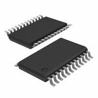
PW PACKAGE
(TOP VIEW)
GND 1
24 GREF
SREF 2
23 DREF
S1 3
22 D1
S2 4
21 D2
S3 5
20 D3
S4 6
19 D4
S5 7
18 D5
S6 8
17 D6
S7 9
16 D7
S8 10
15 D8
S9 11
14 D9
S10 12
13 D10
APPLICATIONS
•
•
•
Bidirectional or Unidirectional Applications
Requiring Voltage-Level Translation From
Any Voltage (1 V to 5 V) to Any Voltage (1 V
to 5 V)
Low Voltage Processor I2C Port Translation
to 3.3-V and/or 5-V I2C Bus Signal Levels
GTL/GTL+ Translation to LVTTL/TTL Signal
Levels
DESCRIPTION/ORDERING INFORMATION
The GTL2010 provides ten NMOS pass transistors (Sn and Dn) with a common gate (GREF) and a reference
transistor (SREF and DREF). The low ON-state resistance of the switch allows connections to be made with
minimal propagation delay. With no direction control pin required, the device allows bidirectional voltage
translations any voltage (1 V to 5 V) to any voltage (1 V to 5 V).
When the Sn or Dn port is LOW, the clamp is in the ON state and a low-resistance connection exists between
the Sn and Dn ports. Assuming the higher voltage is on the Dn port, when the Dn port is HIGH, the voltage on
the Sn port is limited to the voltage set by the reference transistor (SREF). When the Sn port is HIGH, the Dn port
is pulled to VCC by the pullup resistors.
Please be aware that an important notice concerning availability, standard warranty, and use in critical applications of Texas
Instruments semiconductor products and disclaimers thereto appears at the end of this data sheet.
PRODUCTION DATA information is current as of publication date.
Products conform to specifications per the terms of the Texas
Instruments standard warranty. Production processing does not
necessarily include testing of all parameters.
Copyright © 2006, Texas Instruments Incorporated
�GTL2010
10-BIT BIDIRECTIONAL LOW-VOLTAGE TRANSLATOR
www.ti.com
SCDS221 – SEPTEMBER 2006
DESCRIPTION/ORDERING INFORMATION (CONTINUED)
All transistors in the GTL2010 have the same electrical characteristics, and there is minimal deviation from one
output to another in voltage or propagation delay. This offers superior matching over discrete transistor
voltage-translation solutions where the fabrication of the transistors is not symmetrical. With all transistors being
identical, the reference transistor (SREF/DREF) can be located on any of the other ten matched Sn/Dn transistors,
allowing for easier board layout. The translator transistors with integrated ESD circuitry provides excellent ESD
protection.
ORDERING INFORMATION
PACKAGE (1)
TA
–40°C to 85°C
(1)
TSSOP – PW
ORDERABLE PART NUMBER
Tape and reel
SN74GTL2010PWR
GK2010
Package drawings, standard packing quantities, thermal data, symbolization, and PCB design guidelines are available at
www.ti.com/sc/package.
PIN DESCRIPTION
2
TOP-SIDE MARKING
PIN NO.
NAME
DESCRIPTION
1
GND
Ground (0 V)
2
SREF
Source of reference transistor
3–12
Sn
Ports S1–10
13–22
Dn
Ports D10–D1
23
DREF
Drain of reference transistor
24
GREF
Gate of reference transistor
Submit Documentation Feedback
�GTL2010
10-BIT BIDIRECTIONAL LOW-VOLTAGE TRANSLATOR
www.ti.com
SCDS221 – SEPTEMBER 2006
FUNCTION TABLES
(1)
ABC
HIGH-to-LOW Translation (Assuming Dn is at the Higher Voltage Level)
(1)
(2)
(3)
(4)
(5)
GREF (2)
DREF
H
H
0V
H
H
VTT (3)
INPUTS
D10–D1
SREF
OUTPUTS
S10–S1
TRANSISTOR
X
X
Off
H
VTT (4)
On
On
Off
H
H
VTT
L
L (5)
L
L
0 – VTT
X
X
H = HIGH voltage level, L = LOW voltage level, X = don't care
GREF should be at least 1.5 V higher than SREF for best translator operation.
VTT is equal to the SREF voltage.
Sn is not pulled up or pulled down.
Sn follows the Dn input LOW.
LOW-to-HIGH Translation (Assuming Dn is at the Higher Voltage Level) (1)
(1)
(2)
(3)
(4)
(5)
INPUTS
D10–D1
OUTPUTS
S10–S1
GREF (2)
DREF
H
H
0V
X
X
Off
H
H
VTT (3)
VTT
H (4)
Nearly off
H
H
VTT
L
L (5)
On
L
L
0 – VTT
X
X
Off
SREF
TRANSISTOR
H = HIGH voltage level, L = LOW voltage level, X = don't care
GREF should be at least 1.5 V higher than SREF for best translator operation.
VTT is equal to the SREF voltage.
Dn is pulled up to VCC through an external resistor.
Dn follows the Sn input LOW.
CLAMP SCHEMATIC
DREF
SREF
GREF
D1
D10
S1
S10
SA00647
Submit Documentation Feedback
3
�GTL2010
10-BIT BIDIRECTIONAL LOW-VOLTAGE TRANSLATOR
www.ti.com
SCDS221 – SEPTEMBER 2006
Absolute Maximum Ratings (1) (2) (3)
MIN
MAX
UNIT
VSREF
DC source reference voltage
–0.5
7
V
VDREF
DC drain reference voltage
–0.5
7
V
VGREF
DC gate reference voltage
–0.5
7
V
VSn
DC voltage port Sn
–0.5
7
V
VDn
DC voltage port Dn
–0.5
7
IREFK
DC diode current on reference pins
VI < 0 V
–50
mA
ISK
DC diode current port Sn
VI < 0 V
–50
mA
IDK
DC diode current port Dn
VI < 0 V
–50
mA
IMAX
DC clamp current per channel
Channel in ON state
θJA
Package thermal impedance
Tstg
Storage temperature range
(1)
(2)
(3)
±128
–65
V
mA
88
°C/W
150
°C
Stresses beyond those listed under "absolute maximum ratings" may cause permanent damage to the device. These are stress ratings
only, and functional operation of the device at these or any other conditions beyond those indicated under "recommended operating
conditions" is not implied. Exposure to absolute-maximum-rated conditions for extended periods may affect device reliability.
The performance capability of a high-performance integrated circuit in conjunction with its thermal environment can create junction
temperatures that are detrimental to reliability. The maximum junction temperature of this integrated circuit should not exceed 150°C.
The input and output negative voltage ratings may be exceeded if the input and output clamp current ratings are observed.
Recommended Operating Conditions
MIN
MAX
VI/O
Input/output voltage (Sn, Dn)
0
5.5
V
VSREF
DC source reference voltage (1)
0
5.5
V
VDREF
DC drain reference voltage
0
5.5
V
VGREF
DC gate reference voltage
0
5.5
V
IPASS
Pass transistor current
64
mA
Tamb
Operating ambient temperature range (in free air)
85
°C
(1)
4
VSREF = VDREF – 1.5 V for best results in level-shifting applications.
Submit Documentation Feedback
–40
UNIT
�GTL2010
10-BIT BIDIRECTIONAL LOW-VOLTAGE TRANSLATOR
www.ti.com
SCDS221 – SEPTEMBER 2006
Electrical Characteristics
over recommended operating free-air temperature range (unless otherwise noted)
PARAMETER
TEST CONDITIONS
MIN
TYP (1)
MAX
UNIT
260
350
mV
VOL
Low-level output voltage
VDD = 3 V, VSREF = 1.365 V, VSn or VDn = 0.175 V,
Iclamp = 15.2 mA
VIK
Input clamp voltage
II = –18 mA,
VGREF = 0 V
–1.2
V
IIH
Gate input leakage
VI = 5 V,
VGREF = 0 V
5
µA
CI(GREF)
Gate capacitance
VI = 3 V or 0 V
CIO(OFF)
OFF capacitance
VO = 3 V or 0 V,
CIO(ON)
ON capacitance
VO = 3 V or 0 V,
56
pF
VGREF = 0 V
7.4
pF
VGREF = 3 V
18.6
VGREF = 4.5 V
VGREF = 3 V
VI = 0 V
ron (2)
ON-state resistance
VGREF = 1.5 V,
VI = 1.7 V
4.4
7
9
67
105
IO = 30 mA
9
15
7
10
IO = 15 mA
58
80
50
70
VGREF = 4.5 V
VGREF = 3 V
5
5.5
VGREF = 1.5 V
VI = 2.4 V
(1)
(2)
VGREF = 2.3 V
IO = 64 mA
pF
3.5
VGREF = 2.3 V
Ω
All typical values are measured at Tamb = 25°C.
Measured by the voltage drop between the Sn and the Dn terminals at the indicated current through the switch. On-state resistance is
determined by the lowest voltage of the two (Sn or Dn) terminals.
Submit Documentation Feedback
5
�GTL2010
10-BIT BIDIRECTIONAL LOW-VOLTAGE TRANSLATOR
www.ti.com
SCDS221 – SEPTEMBER 2006
AC Characteristics for Translator-Type Applications (1)
VREF = 1.365 V to 1.635 V, VDD1 = 3 V to 3.6 V, VDD2 = 2.36 V to 2.64 V, GND = 0 V, tr = tf ≤ 3 ns, Tamb = –40°C to 85°C
(see Figure 5)
PARAMETER
tPLH
(1)
(2)
(3)
(3)
MIN
TYP (2)
MAX
0.5
1.5
5.5
Propagation delay (Sn to Dn, Dn to Sn)
CON(max) of 30 pF and a COFF(max) of 15 pF is specified by design.
All typical values are measured at VDD1 = 3.3 V, VDD2 = 2.5 V, VREF = 1.5 V and Tamb = 25°C.
Propagation delay specified by characterization.
AC Waveforms
Vm = 1.5 V, VIN = GND to 3 V
VI
Input
VM
VM
tPHL0
tPLH0
GND
VDD2
VM
Low-to-High
VOL
VM
tPHL
tPLH
tPHL1
VDD2
tPLH1
VM
Low-to-High
VOL
VM
Figure 1. Input (Sn) to Output (Dn) Propagation Delays
VDD2
VDD2
200 W
150 W
VDD2
VDD2
150 W
150 W
DUT
DREF GREF
D1 . . . D10
SREF
S1 . . . S10
Test
Jig
VREF
Pulse
Generator
Figure 2. Load Circuit
6
Submit Documentation Feedback
UNIT
ns
�GTL2010
10-BIT BIDIRECTIONAL LOW-VOLTAGE TRANSLATOR
www.ti.com
SCDS221 – SEPTEMBER 2006
AC Characteristics for CBT-Type Applications
GND = 0 V, tR, CL = 50 pF, GREF = 5 V ± 0.5 V, Tamb = –40°C to 85°C
PARAMETER
tpd
(1)
MIN
Propagation delay (1)
MAX
UNIT
250
ps
This parameter is warranted but not production tested. The propagation delay is based on the RC time constant of the typical on-state
resistance of the switch and a load capacitance of 50 pF, when driven by an ideal voltage source (zero output impedance).
AC Waveforms
3V
Input
1.5 V
1.5 V
tPLH
tPHL
0V
VOH
1.5 V
Output
1.5 V
VOL
Figure 3. Input (Sn) to Output (Dn) Propagation Delays
500 W
From Ouput
Under Test
CL = 50 pF
S1
7V
500 W
Load Circuit
TEST
tpd
S1
Open
tPLZ/tPZL
7V
tPHZ/tPZH
Open
CL = Load capacitance, includes jig and probe capacitance
(see AC Characteristics for value).
Figure 4. Load Circuit
Submit Documentation Feedback
7
�GTL2010
10-BIT BIDIRECTIONAL LOW-VOLTAGE TRANSLATOR
www.ti.com
SCDS221 – SEPTEMBER 2006
APPLICATION INFORMATION
Bidirectional Translation
For the bidirectional clamping configuration (higher voltage to lower voltage or lower voltage to higher voltage),
the GREF input must be connected to DREF and both pins pulled to HIGH-side VCC through a pullup resistor
(typically 200 kΩ). A filter capacitor on DREF is recommended. The processor output can be totem pole or open
drain (pullup resistors) and the chipset output can be totem pole or open drain (pullup resistors are required to
pull the Dn outputs to VCC). However, if either output is totem pole, data must be unidirectional or the outputs
must be 3-statable, and the outputs must be controlled by some direction-control mechanism to prevent
HIGH-to-LOW contentions in either direction. If both outputs are open drain, no direction control is needed. The
opposite side of the reference transistor (SREF) is connected to the processor core power-supply voltage. When
DREF is connected through a 200-kΩ resistor to a 3.3-V to 5.5-V VCC supply and SREF is set between 1 V to VCC
1.5 V, the output of each Sn has a maximum output voltage equal to SREF, and the output of each Dn has a
maximum output voltage equal to VCC.
8
Submit Documentation Feedback
�GTL2010
10-BIT BIDIRECTIONAL LOW-VOLTAGE TRANSLATOR
www.ti.com
SCDS221 – SEPTEMBER 2006
APPLICATION INFORMATION (continued)
VDPU = 5V
200K Ω
VREF = 1.8V
GTL2010
GREF
RPU
RPU
RPU
DREF
SREF
RPU
S1
D1
SW
CPU I/O
Chipset
I/O
S2
D2
SW
VDPU = 3.3V
RPU
S9
RPU
D9
Chipset
I/O
S10
D10
GND
Figure 5. Bidirectional Translation to Multiple Higher Voltage Levels (Such as an I2C or SMBus
Applications)
Submit Documentation Feedback
9
�GTL2010
10-BIT BIDIRECTIONAL LOW-VOLTAGE TRANSLATOR
www.ti.com
SCDS221 – SEPTEMBER 2006
APPLICATION INFORMATION (continued)
Unidirectional Down Translation
For unidirectional clamping (higher voltage to lower voltage), the GREF input must be connected to DREF and both
pins pulled to the higher-side VCC through a pullup resistor (typically 200 kΩ). A filter capacitor on DREF is
recommended. Pullup resistors are required if the chipset I/Os are open drain. The opposite side of the
reference transistor (SREF) is connected to the processor core power-supply voltage. When DREF is connected
through a 200-kΩ resistor to a 3.3-V to 5.5-V VCC supply and SREF is set between 1 V to VCC – 1.5 V, the output
of each Sn has a maximum output voltage equal to SREF.
VDPU = 5V
200K Ω
GTL2010
VREF = 1.8V
DREF
SREF
S1
GREF
SW
D1
CPU I/O
S2
D2
Chipset
I/O
SW
Sn
Dn
GND
Figure 6. Unidirectional Down Translation to Protect Low-Voltage Processor Pins
10
Submit Documentation Feedback
�GTL2010
10-BIT BIDIRECTIONAL LOW-VOLTAGE TRANSLATOR
www.ti.com
SCDS221 – SEPTEMBER 2006
APPLICATION INFORMATION (continued)
Unidirectional Up Translation
For unidirectional up translation (lower voltage to higher voltage), the reference transistor is connected the same
as for a down translation. A pullup resistor is required on the higher voltage side (Dn or Sn) to get the full HIGH
level, since the GTL device only passes the reference source (SREF) voltage as a HIGH when doing an up
translation. The driver on the lower voltage side only needs pullup resistors if it is open drain.
VDPU = 5V
200K Ω
GTL2010
VREF = 1.8V
GREF
RPU
RPU
RPU
DREF
SREF
RPU
S1
SW
D1
CPU I/O
Chipset
I/O
S2
SW
Sn
D2
Dn
GND
Figure 7. Unidirectional Up Translation to Higher-Voltage Chipsets
Submit Documentation Feedback
11
�GTL2010
10-BIT BIDIRECTIONAL LOW-VOLTAGE TRANSLATOR
www.ti.com
SCDS221 – SEPTEMBER 2006
APPLICATION INFORMATION (continued)
Sizing Pullup Resistor
The pullup resistor value should limit the current through the pass transistor when it is in the on state to about
15 mA. This ensures a pass voltage of 260 mV to 350 mV. If the current through the pass transistor is higher
than 15 mA, the pass voltage also is higher in the on state. To set the current through each pass transistor at
15 mA, the pullup resistor value is calculated as:
Resistor value (W) +
Pullup voltage (V) * 0.35 V
0.015 A
Table 1 shows resistor values for various reference voltages and currents at 15 mA, 10 mA, and 3 mA. The
resistor value shown in the +10% column, or a larger value, should be used to ensure that the pass voltage of
the transistor would be 350 mV or less. The external driver must be able to sink the total current from the
resistors on both sides of the GTL device at 0.175 V, although the 15 mA only applies to current flowing through
the GTL2010.
Table 1. Pullup Resistor Values (1) (2) (3)
PULLUP RESISTOR VALUE (Ω)
VOLTAGE
(1)
(2)
(3)
12
15 mA
10 mA
3 mA
NOMINAL
+10%
NOMINAL
+10%
NOMINAL
+10%
5.0 V
310
341
465
512
1550
1705
3.3 V
197
217
295
325
983
1082
2.5 V
143
158
215
237
717
788
1.8 V
97
106
145
160
483
532
1.5 V
77
85
115
127
383
422
1.2 V
57
63
85
94
283
312
Calculated for VOL = 0.35 V
Assumes output driver VOL = 0.175 V at stated current
+10% to compensate for VDD range and resistor tolerance
Submit Documentation Feedback
�PACKAGE OPTION ADDENDUM
www.ti.com
10-Dec-2020
PACKAGING INFORMATION
Orderable Device
Status
(1)
Package Type Package Pins Package
Drawing
Qty
Eco Plan
(2)
Lead finish/
Ball material
MSL Peak Temp
Op Temp (°C)
Device Marking
(3)
(4/5)
(6)
SN74GTL2010PW
ACTIVE
TSSOP
PW
24
60
RoHS & Green
NIPDAU
Level-1-260C-UNLIM
-40 to 85
GK2010
SN74GTL2010PWR
ACTIVE
TSSOP
PW
24
2000
RoHS & Green
NIPDAU
Level-1-260C-UNLIM
-40 to 85
GK2010
(1)
The marketing status values are defined as follows:
ACTIVE: Product device recommended for new designs.
LIFEBUY: TI has announced that the device will be discontinued, and a lifetime-buy period is in effect.
NRND: Not recommended for new designs. Device is in production to support existing customers, but TI does not recommend using this part in a new design.
PREVIEW: Device has been announced but is not in production. Samples may or may not be available.
OBSOLETE: TI has discontinued the production of the device.
(2)
RoHS: TI defines "RoHS" to mean semiconductor products that are compliant with the current EU RoHS requirements for all 10 RoHS substances, including the requirement that RoHS substance
do not exceed 0.1% by weight in homogeneous materials. Where designed to be soldered at high temperatures, "RoHS" products are suitable for use in specified lead-free processes. TI may
reference these types of products as "Pb-Free".
RoHS Exempt: TI defines "RoHS Exempt" to mean products that contain lead but are compliant with EU RoHS pursuant to a specific EU RoHS exemption.
Green: TI defines "Green" to mean the content of Chlorine (Cl) and Bromine (Br) based flame retardants meet JS709B low halogen requirements of