��������
��
�
��� �����
��
���� ����������
����
���� ���������� �����������
���� ����� ����� ���� ��� �������� ����
SCES352C − JUNE 2001 − REVISED SEPTEMBER 2001
D Member of the Texas Instruments
D
D
D
D
D
D
D
D
D
D
D
D
Widebus Family
TI-OPC Circuitry Limits Ringing on
Unevenly Loaded Backplanes
OEC Circuitry Improves Signal Integrity
and Reduces Electromagnetic Interference
Bidirectional Interface Between GTLP
Signal Levels and LVTTL Logic Levels
Split LVTTL Port Provides a Feedback Path
for Control and Diagnostics Monitoring
LVTTL Interfaces Are 5-V Tolerant
High-Drive GTLP Open-Drain Outputs
(100 mA)
LVTTL Outputs (−24 mA/24 mA)
Variable Edge-Rate Control (ERC) Input
Selects GTLP Rise and Fall Times for
Optimal Data-Transfer Rate and Signal
Integrity in Distributed Loads
Ioff, Power-Up 3-State, and BIAS VCC
Support Live Insertion
Distributed VCC and GND Pins Minimize
High-Speed Switching Noise
Latch-Up Performance Exceeds 100 mA Per
JESD 78, Class II
ESD Protection Exceeds JESD 22
− 2000-V Human-Body Model (A114-A)
− 1000-V Charged-Device Model (C101)
DGG OR DGV PACKAGE
(TOP VIEW)
IMODE1
AI1
AO1
GND
AI2
AO2
VCC
AI3
AO3
GND
AI4
AO4
AO5
AI5
GND
AO6
AI6
VCC
AO7
AI7
GND
AO8
AI8
OMODE0
1
48
2
47
3
46
4
45
5
44
6
43
7
42
8
41
9
40
10
39
11
38
12
37
13
36
14
35
15
34
16
33
17
32
18
31
19
30
20
29
21
28
22
27
23
26
24
25
IMODE0
BIAS VCC
B1
GND
OEAB
B2
ERC
OEAB
B3
GND
CLKAB/LEAB
B4
B5
CLKBA/LEBA
GND
B6
OEBA
VCC
B7
LOOPBACK
GND
B8
VREF
OMODE1
description
The SN74GTLP2033 is a high-drive, 8-bit, three-wire registered transceiver that provides inverted
LVTTL-to-GTLP and GTLP-to-LVTTL signal-level translation. The device allows for transparent, latched, and
flip-flop modes of data transfer with separate LVTTL input and LVTTL output pins, which provides a feedback
path for control and diagnostics monitoring, the same functionality as the SN74FB2033. The device provides
a high-speed interface between cards operating at LVTTL logic levels and a backplane operating at GTLP signal
levels. High-speed (about three times faster than standard LVTTL or TTL) backplane operation is a direct result
of GTLP’s reduced output swing ( VCC.
3. The package thermal impedance is calculated in accordance with JESD 51-7.
POST OFFICE BOX 655303
• DALLAS, TEXAS 75265
7
���������
��
�
��� �����
��
���� ����������
����
���� ���������� �����������
���� ����� ����� ���� ��� �������� ����
SCES352C − JUNE 2001 − REVISED SEPTEMBER 2001
recommended operating conditions (see Notes 4 through 7)
VCC,
BIAS VCC
Supply voltage
VTT
Termination voltage
VREF
Reference voltage
VI
Input voltage
VIH
High-level input voltage
VIL
Low-level input voltage
IIK
IOH
Input clamp current
MIN
NOM
MAX
UNIT
3.15
3.3
3.45
V
GTL
1.14
1.2
1.26
GTLP
1.35
1.5
1.65
GTL
0.74
0.8
0.87
GTLP
0.87
1
1.1
VCC
VTT
5.5
B port
Except B port and VREF
B port
Except B port
VREF+0.05
2
B port
High-level output current
IOL
Low-level output current
∆t/∆v
Input transition rise or fall rate
∆t/∆VCC
TA
Power-up ramp rate
V
V
V
VREF−0.05
0.8
Except B port
V
V
−18
mA
AO
−24
mA
AO
24
B port
100
Outputs enabled
10
−40
ns/V
µs/V
20
Operating free-air temperature
mA
85
°C
NOTES: 4. All unused control and B-port inputs of the device must be held at VCC or GND to ensure proper device operation. Refer to the TI
application report, Implications of Slow or Floating CMOS Inputs, literature number SCBA004.
5. Proper connection sequence for use of the B-port I/O precharge feature is GND and BIAS VCC = 3.3 V first, I/O second, and
VCC = 3.3 V last, because the BIAS VCC precharge circuitry is disabled when any VCC pin is connected. The control and VREF inputs
can be connected anytime, but normally are connected during the I/O stage. If B-port precharge is not required, any connection
sequence is acceptable but, generally, GND is connected first.
6. VTT and RTT can be adjusted to accommodate backplane impedances if the dc recommended IOL ratings are not exceeded.
7. VREF can be adjusted to optimize noise margins, but normally is two-thirds VTT. TI-OPC circuitry is enabled in the A-to-B direction
and is activated when VTT > 0.7 V above VREF. If operated in the A-to-B direction, VREF should be set to within 0.6 V of VTT to
minimize current drain.
8
POST OFFICE BOX 655303
• DALLAS, TEXAS 75265
���������
��
�
��� �����
��
���� ����������
����
���� ���������� �����������
���� ����� ����� ���� ��� �������� ����
SCES352C − JUNE 2001 − REVISED SEPTEMBER 2001
electrical characteristics over recommended operating free-air temperature range for GTLP
(unless otherwise noted)
PARAMETER
VIK
VOH
AO
TEST CONDITIONS
VCC = 3.15 V,
VCC = 3.15 V to 3.45 V,
II = −18 mA
IOH = −100 µA
VCC = 3.15 V
IOH = −12 mA
IOH = −24 mA
VCC = 3.15 V to 3.45 V,
AO
VCC = 3.15 V
VOL
B port
II‡
IOZ‡
ICC
MIN
VCC = 3.15 V
TYP†
MAX
UNIT
−1.2
V
VCC−0.2
2.4
V
2
IOL = 100 µA
IOL = 12 mA
0.2
IOL = 24 mA
IOL = 10 mA
0.5
IOL = 64 mA
IOL = 100 mA
0.4
0.55
0.4
0.2
AI and
control inputs
VCC = 3.45 V,
VI = 0 or 5.5 V
±10
AO
VCC = 3.45 V,
VO = 0 to 5.5 V
±10
B port
VCC = 3.45 V, VREF within 0.6 V of VTT,
VO = 0 to 2.3 V
±10
VCC = 3.45 V, IO = 0,
VI (A-port or control input) = VCC or GND,
VI (B port) = VTT or GND
Outputs high
40
AO or B port
Outputs low
40
Outputs disabled
40
VCC = 3.45 V, One AI or control input at VCC − 0.6 V,
Other AI or control inputs at VCC or GND
∆ICC§
AI
Ci
Control inputs
Co
AO
Cio
B port
1.5
V
µA
µA
A
mA
mA
3.5
4.5
VI = 3.15 V or 0
3.5
5.5
VO = 3.15 V or 0
VO = 1.5 V or 0
5
6
pF
8.5
10
pF
pF
† All typical values are at VCC = 3.3 V, TA = 25°C.
‡ For I/O ports, the parameter IOZ includes the input leakage current.
§ This is the increase in supply current for each input that is at the specified TTL voltage level rather than VCC or GND.
hot-insertion specifications for A port over recommended operating free-air temperature range
PARAMETER
TEST CONDITIONS
Ioff
IOZPU
VCC = 0,
VCC = 0 to 1.5 V,
VI or VO = 0 to 5.5 V
VO = 0.5 V to 3 V,
IOZPD
VCC = 1.5 V to 0,
VO = 0.5 V to 3 V,
MIN
MAX
UNIT
10
µA
OEBA = VCC
±30
µA
OEBA = VCC
±30
µA
live-insertion specifications for B port over recommended operating free-air temperature range
PARAMETER
TEST CONDITIONS
Ioff
IOZPU
VCC = 0,
BIAS VCC = 0,
VI or VO = 0 to 1.5 V
VCC = 0 to 1.5 V, BIAS VCC = 0, VO = 0.5 V to 1.5 V, OEAB = 0 and OEAB = VCC
IOZPD
VCC = 1.5 V to 0, BIAS VCC = 0, VO = 0.5 V to 1.5 V, OEAB = 0 and OEAB = VCC
VCC = 0 to 3.15 V
BIAS VCC = 3.15 V to 3.45 V, VO (B port) = 0 to 1.5 V
VCC = 3.15 V to 3.45 V
VCC = 0,
BIAS VCC = 3.3 V,
IO = 0
ICC
(BIAS VCC)
VO
IO
VCC = 0,
BIAS VCC = 3.15 V to 3.45 V,
POST OFFICE BOX 655303
VO (B port) = 0.6 V
• DALLAS, TEXAS 75265
MIN
0.95
−1
MAX
UNIT
10
µA
±30
µA
±30
µA
5
mA
10
µA
1.05
V
µA
9
���������
��
�
��� �����
��
���� ����������
����
���� ���������� �����������
���� ����� ����� ���� ��� �������� ����
SCES352C − JUNE 2001 − REVISED SEPTEMBER 2001
timing requirements over recommended ranges of supply voltage and operating free-air
temperature, VTT = 1.5 V and VREF = 1 V for GTLP (unless otherwise noted)
MIN
fclock
tw
Clock frequency
Pulse duration
CLKAB/LEAB or CLKBA/LEBA
2.8
AI before CLKAB↑
1.1
AI before CLKBA↑
1.4
B before CLKBA↑
tsu
th
10
Setup time
Hold time
POST OFFICE BOX 655303
UNIT
175
MHz
ns
1
AI before LEAB↓
1.6
AI before LEBA↓
2.1
B before LEBA↓
2.2
AI after CLKAB↑
0.3
AI after CLKBA↑
0.2
B after CLKBA↑
0.6
AI after LEAB↓
0.3
AI after LEBA↓
0
B after LEBA↓
0
• DALLAS, TEXAS 75265
MAX
ns
ns
���������
��
�
��� �����
��
���� ����������
����
���� ���������� �����������
���� ����� ����� ���� ��� �������� ����
SCES352C − JUNE 2001 − REVISED SEPTEMBER 2001
switching characteristics over recommended ranges of supply voltage and operating free-air
temperature, VTT = 1.5 V and VREF = 1 V for GTLP (see Figure 1)
PARAMETER
FROM
(INPUT)
TO
(OUTPUT)
EDGE RATE†
fmax
MIN
TYP‡
MAX
175
tPLH
tPHL
AI
(buffer)
B
Slow
tPLH
tPHL
AI
(buffer)
B
Fast
tPLH
tPHL
B
(buffer)
AO
−
tPLH
tPHL
LEAB
(latch mode)
B
Slow
tPLH
tPHL
LEAB
(latch mode)
B
Fast
tPLH
tPHL
LEAB
(latch mode)
AO
−
tPLH
tPHL
LEBA
(latch mode)
AO
−
tPLH
tPHL
OEAB
B
Slow
tPLH
tPHL
OEAB
B
Fast
tPLH
tPHL
OEAB
B
Slow
tPLH
tPHL
OEAB
B
Fast
tPZH
tPZL
OEBA
AO
−
tPHZ
tPLZ
OEBA
AO
−
tPLH
tPHL
CLKAB
(flip-flop mode)
B
Slow
tPLH
tPHL
CLKAB
(flip-flop mode)
B
Fast
tPLH
tPHL
CLKAB
(flip-flop mode)
AO
−
tPLH
tPHL
CLKBA
(flip-flop mode)
AO
−
tPLH
tPHL
OMODE
B
Slow
tPLH
tPHL
OMODE
B
Fast
tPLH
tPHL
IMODE
AO
−
UNIT
MHz
3
7.4
3
7.1
2
5.9
2
5.8
1
5.7
1
5
4.2
8.6
3.2
7.7
3.2
7.6
2.8
6.7
2
7
1.8
6.3
1
5.7
1
4.7
3.8
7.5
3.1
7
2.5
6
2.5
6
3.5
7.5
3
7.2
2.5
6
2.5
6
1
4.7
1
3.4
1
5.2
1
4.9
4.4
8.8
3.6
8.1
3.2
7.2
3.1
6.9
2
6.9
1.8
6.4
1
5.6
1
4.9
3.8
8.7
3.2
8.2
2.7
7.2
2.7
7.2
1
5.6
1
4.6
ns
ns
ns
ns
ns
ns
ns
ns
ns
ns
ns
ns
ns
ns
ns
ns
ns
ns
ns
ns
† Slow (ERC = H) and Fast (ERC = L)
‡ All typical values are at VCC = 3.3 V, TA = 25°C.
POST OFFICE BOX 655303
• DALLAS, TEXAS 75265
11
���������
��
�
��� �����
��
���� ����������
����
���� ���������� �����������
���� ����� ����� ���� ��� �������� ����
SCES352C − JUNE 2001 − REVISED SEPTEMBER 2001
switching characteristics over recommended ranges of supply voltage and operating free-air
temperature, VTT = 1.5 V and VREF = 1 V for GTLP (see Figure 1) (continued)
PARAMETER
FROM
(INPUT)
TO
(OUTPUT)
EDGE RATE†
tPLH
tPHL
LOOPBACK
AO
−
tPLH
tPHL
AI
(loopback high)
AO
−
tr
Rise time, B-port outputs (20% to 80%)
MIN
TYP‡
MAX
2.5
6.2
6.2
2
5
5
1
5.6
5.6
1
5
5
Slow
2.8
Fast
1.5
Rise time, AO (10% to 90%)
tf
UNIT
ns
ns
ns
3.5
Fall time, B-port outputs (80% to 20%)
Slow
3
Fast
1.8
Fall time, AO (90% to 10%)
ns
1.5
† Slow (ERC = H) and Fast (ERC = L)
‡ All typical values are at VCC = 3.3 V, TA = 25°C.
skew characteristics over recommended ranges of supply voltage and operating free-air
temperature (see Figure 1)§
PARAMETER
tsk(LH)¶
tsk(HL)¶
tsk(LH)¶
tsk(HL)¶
tsk(LH)¶
tsk(HL)¶
tsk(LH)¶
tsk(HL)¶
FROM
(INPUT)
TO
(OUTPUT)
EDGE RATE†
AI
B
Slow
AI
B
CLKAB/LEAB
CLKAB/LEAB
AI
B
B
B
tsk(t)¶
CLKAB/LEAB
B
TYP‡
MAX
0.5
1
0.5
1
0.4
0.9
0.4
0.9
0.5
1
0.5
1
0.4
0.9
0.4
0.9
Slow
1.4
2
Fast
0.6
1.4
Slow
1.8
2.5
Fast
0.9
1.8
MIN
UNIT
ns
Fast
ns
Slow
ns
Fast
ns
ns
† Slow (ERC = L) and Fast (ERC = H)
‡ All typical values are at VCC = 3.3 V, TA = 25°C.
§ Actual skew values between the GTLP outputs could vary on the backplane due to the loading and impedance seen by the device.
¶ tsk(LH)/tsk(HL) and tsk(t) − Output-to-output skew is defined as the absolute value of the difference between the actual propagation delay for all
outputs with the same packaged device. The specifications are given for specific worst-case VCC and temperature and apply to any outputs
switching in the same direction either high to low [tsk(HL)] or low to high [tsk(LH)] or in opposite directions, both low to high and high to low [tsk(t)].
12
POST OFFICE BOX 655303
• DALLAS, TEXAS 75265
���������
��
�
��� �����
��
���� ����������
����
���� ���������� �����������
���� ����� ����� ���� ��� �������� ����
SCES352C − JUNE 2001 − REVISED SEPTEMBER 2001
PARAMETER MEASUREMENT INFORMATION
1.5 V
6V
S1
500 Ω
From Output
Under Test
Open
GND
CL = 50 pF
(see Note A)
500 Ω
12.5 Ω
S1
Open
6V
GND
TEST
tPLH/tPHL
tPLZ/tPZL
tPHZ/tPZH
From Output
Under Test
Test
Point
CL = 30 pF
(see Note A)
LOAD CIRCUIT FOR B OUTPUTS
LOAD CIRCUIT FOR A OUTPUTS
tw
3V
3V
1.5 V
Input
1.5 V
Timing
Input
1.5 V
0V
0V
VOLTAGE WAVEFORMS
PULSE DURATION
tsu
th
VOH
Data
Input
VM
VM
0V
3V
Input
1.5 V
1.5 V
0V
tPLH
tPHL
VOLTAGE WAVEFORMS
SETUP AND HOLD TIMES
(VM = 1.5 V for A port and 1 V for B port)
(VOH = 3 V for A port and 1.5 V for B port)
VOH
1V
Output
1V
3V
VOL
VOLTAGE WAVEFORMS
PROPAGATION DELAY TIMES
(AI to B port)
1V
1V
0V
tPLH
1.5 V
1.5 V
0V
Output
Waveform 1
S1 at 6 V
(see Note B)
tPLZ
3V
1.5 V
VOL + 0.3 V
VOL
tPHZ
tPZH
tPHL
VOH
Output
1.5 V
tPZL
1.5 V
Input
Output
Control
1.5 V
VOL
Output
Waveform 2
S1 at GND
(see Note B)
1.5 V
VOH
VOH − 0.3 V
≈0 V
VOLTAGE WAVEFORMS
ENABLE AND DISABLE TIMES
(AO)
VOLTAGE WAVEFORMS
PROPAGATION DELAY TIMES
(B port to AO)
NOTES: A. CL includes probe and jig capacitance.
B. Waveform 1 is for an output with internal conditions such that the output is low except when disabled by the output control.
Waveform 2 is for an output with internal conditions such that the output is high except when disabled by the output control.
C. All input pulses are supplied by generators having the following characteristics: PRR ≈ 10 MHz, ZO = 50 Ω, tr ≈ 2 ns, tf ≈ 2 ns.
D. The outputs are measured one at a time with one transition per measurement.
Figure 1. Load Circuits and Voltage Waveforms
POST OFFICE BOX 655303
• DALLAS, TEXAS 75265
13
���������
��
�
��� �����
��
���� ����������
����
���� ���������� �����������
���� ����� ����� ���� ��� �������� ����
SCES352C − JUNE 2001 − REVISED SEPTEMBER 2001
DISTRIBUTED-LOAD BACKPLANE SWITCHING CHARACTERISTICS
The preceding switching characteristics table shows the switching characteristics of the device into a lumped load
(Figure 1). However, the designer’s backplane application is probably a distributed load. The physical representation
is shown in Figure 2. This backplane, or distributed load, can be approximated closely to a resistor inductance
capacitance (RLC) circuit, as shown in Figure 3. This device has been designed for optimum performance in this RLC
circuit. The following switching characteristics table shows the switching characteristics of the device into the RLC
load, to help the designer to better understand the performance of the GTLP device in this typical backplane. See
www.ti.com/sc/gtlp for more information.
1.5 V
ZO = 50 Ω
.25”
1”
1.5 V
1”
.25”
22 Ω
22 Ω
1.5 V
11 Ω
Conn.
1”
Conn.
1”
Conn.
1”
Conn.
From Output
Under Test
1”
Rcvr
Rcvr
Rcvr
Slot 2
Slot 19
Slot 20
LL = 14 nH
Test
Point
CL = 18 pF
Drvr
Slot 1
Figure 2. High-Drive Test Backplane
14
POST OFFICE BOX 655303
Figure 3. High-Drive RLC Network
• DALLAS, TEXAS 75265
���������
��
�
��� �����
��
���� ����������
����
���� ���������� �����������
���� ����� ����� ���� ��� �������� ����
SCES352C − JUNE 2001 − REVISED SEPTEMBER 2001
switching characteristics over recommended operating conditions for the bus transceiver
function (unless otherwise noted) (see Figure 3)
PARAMETER
FROM
(INPUT)
TO
(OUTPUT)
EDGE RATE†
tPLH
tPHL
AI
(buffer)
B
Slow
tPLH
tPHL
AI
(buffer)
B
Fast
tPLH
tPHL
LEAB
(latch mode)
B
Slow
tPLH
tPHL
LEAB
(latch mode)
B
Fast
tPLH
tPHL
CLKAB
(flip-flop mode)
B
Slow
tPLH
tPHL
CLKAB
(flip-flop mode)
B
Fast
tPLH
tPHL
OMODE
B
Slow
tPLH
tPHL
OMODE
B
Fast
TYP‡
UNIT
4.7
5
ns
3.7
4
ns
5.5
5.8
ns
4.6
4.8
ns
5.8
6
ns
4.9
4.9
ns
5.5
5.7
ns
4.5
tr
Rise time, B-port outputs (20% to 80%)
tf
Fall time, B-port outputs (80% to 20%)
4.7
Slow
1.8
Fast
1.1
Slow
3.4
Fast
2.6
ns
ns
ns
† Slow (ERC = H) and Fast (ERC = L)
‡ All typical values are at VCC = 3.3 V, TA = 25°C. All values are derived from TI-SPICE models.
POST OFFICE BOX 655303
• DALLAS, TEXAS 75265
15
�PACKAGE OPTION ADDENDUM
www.ti.com
25-Jan-2013
PACKAGING INFORMATION
Orderable Device
Status
(1)
Package Type Package Pins Package Qty
Drawing
Eco Plan
Lead/Ball Finish
(2)
MSL Peak Temp
Op Temp (°C)
Top-Side Markings
(3)
(4)
74GTLP2033DGGRE4
ACTIVE
TSSOP
DGG
48
2000
Green (RoHS
& no Sb/Br)
CU NIPDAU
Level-1-260C-UNLIM
-40 to 85
GTLP2033
74GTLP2033DGGRG4
ACTIVE
TSSOP
DGG
48
2000
Green (RoHS
& no Sb/Br)
CU NIPDAU
Level-1-260C-UNLIM
-40 to 85
GTLP2033
SN74GTLP2033DGGR
ACTIVE
TSSOP
DGG
48
2000
Green (RoHS
& no Sb/Br)
CU NIPDAU
Level-1-260C-UNLIM
-40 to 85
GTLP2033
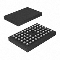
SN74GTLP2033ZQLR
ACTIVE
BGA
MICROSTAR
JUNIOR
ZQL
56
TBD
Call TI
Call TI
-40 to 85
GR033
(1)
The marketing status values are defined as follows:
ACTIVE: Product device recommended for new designs.
LIFEBUY: TI has announced that the device will be discontinued, and a lifetime-buy period is in effect.
NRND: Not recommended for new designs. Device is in production to support existing customers, but TI does not recommend using this part in a new design.
PREVIEW: Device has been announced but is not in production. Samples may or may not be available.
OBSOLETE: TI has discontinued the production of the device.
(2)
Eco Plan - The planned eco-friendly classification: Pb-Free (RoHS), Pb-Free (RoHS Exempt), or Green (RoHS & no Sb/Br) - please check http://www.ti.com/productcontent for the latest availability
information and additional product content details.
TBD: The Pb-Free/Green conversion plan has not been defined.
Pb-Free (RoHS): TI's terms "Lead-Free" or "Pb-Free" mean semiconductor products that are compatible with the current RoHS requirements for all 6 substances, including the requirement that
lead not exceed 0.1% by weight in homogeneous materials. Where designed to be soldered at high temperatures, TI Pb-Free products are suitable for use in specified lead-free processes.
Pb-Free (RoHS Exempt): This component has a RoHS exemption for either 1) lead-based flip-chip solder bumps used between the die and package, or 2) lead-based die adhesive used between
the die and leadframe. The component is otherwise considered Pb-Free (RoHS compatible) as defined above.
Green (RoHS & no Sb/Br): TI defines "Green" to mean Pb-Free (RoHS compatible), and free of Bromine (Br) and Antimony (Sb) based flame retardants (Br or Sb do not exceed 0.1% by weight
in homogeneous material)
(3)
MSL, Peak Temp. -- The Moisture Sensitivity Level rating according to the JEDEC industry standard classifications, and peak solder temperature.
(4)
Only one of markings shown within the brackets will appear on the physical device.
Important Information and Disclaimer:The information provided on this page represents TI's knowledge and belief as of the date that it is provided. TI bases its knowledge and belief on information
provided by third parties, and makes no representation or warranty as to the accuracy of such information. Efforts are underway to better integrate information from third parties. TI has taken and
continues to take reasonable steps to provide representative and accurate information but may not have conducted destructive testing or chemical analysis on incoming materials and chemicals.
TI and TI suppliers consider certain information to be proprietary, and thus CAS numbers and other limited information may not be available for release.
In no event shall TI's liability arising out of such information exceed the total purchase price of the TI part(s) at issue in this document sold by TI to Customer on an annual basis.
Addendum-Page 1
Samples
�PACKAGE OPTION ADDENDUM
www.ti.com
25-Jan-2013
Addendum-Page 2
��MECHANICAL DATA
MTSS003D – JANUARY 1995 – REVISED JANUARY 1998
DGG (R-PDSO-G**)
PLASTIC SMALL-OUTLINE PACKAGE
48 PINS SHOWN
0,27
0,17
0,50
48
0,08 M
25
6,20
6,00
8,30
7,90
0,15 NOM
Gage Plane
1
0,25
24
0°– 8°
A
0,75
0,50
Seating Plane
0,15
0,05
1,20 MAX
PINS **
0,10
48
56
64
A MAX
12,60
14,10
17,10
A MIN
12,40
13,90
16,90
DIM
4040078 / F 12/97
NOTES: A.
B.
C.
D.
All linear dimensions are in millimeters.
This drawing is subject to change without notice.
Body dimensions do not include mold protrusion not to exceed 0,15.
Falls within JEDEC MO-153
POST OFFICE BOX 655303
• DALLAS, TEXAS 75265
�IMPORTANT NOTICE
Texas Instruments Incorporated and its subsidiaries (TI) reserve the right to make corrections, enhancements, improvements and other
changes to its semiconductor products and services per JESD46, latest issue, and to discontinue any product or service per JESD48, latest
issue. Buyers should obtain the latest relevant information before placing orders and should verify that such information is current and
complete. All semiconductor products (also referred to herein as “components”) are sold subject to TI’s terms and conditions of sale
supplied at the time of order acknowledgment.
TI warrants performance of its components to the specifications applicable at the time of sale, in accordance with the warranty in TI’s terms
and conditions of sale of semiconductor products. Testing and other quality control techniques are used to the extent TI deems necessary
to support this warranty. Except where mandated by applicable law, testing of all parameters of each component is not necessarily
performed.
TI assumes no liability for applications assistance or the design of Buyers’ products. Buyers are responsible for their products and
applications using TI components. To minimize the risks associated with Buyers’ products and applications, Buyers should provide
adequate design and operating safeguards.
TI does not warrant or represent that any license, either express or implied, is granted under any patent right, copyright, mask work right, or
other intellectual property right relating to any combination, machine, or process in which TI components or services are used. Information
published by TI regarding third-party products or services does not constitute a license to use such products or services or a warranty or
endorsement thereof. Use of such information may require a license from a third party under the patents or other intellectual property of the
third party, or a license from TI under the patents or other intellectual property of TI.
Reproduction of significant portions of TI information in TI data books or data sheets is permissible only if reproduction is without alteration
and is accompanied by all associated warranties, conditions, limitations, and notices. TI is not responsible or liable for such altered
documentation. Information of third parties may be subject to additional restrictions.
Resale of TI components or services with statements different from or beyond the parameters stated by TI for that component or service
voids all express and any implied warranties for the associated TI component or service and is an unfair and deceptive business practice.
TI is not responsible or liable for any such statements.
Buyer acknowledges and agrees that it is solely responsible for compliance with all legal, regulatory and safety-related requirements
concerning its products, and any use of TI components in its applications, notwithstanding any applications-related information or support
that may be provided by TI. Buyer represents and agrees that it has all the necessary expertise to create and implement safeguards which
anticipate dangerous consequences of failures, monitor failures and their consequences, lessen the likelihood of failures that might cause
harm and take appropriate remedial actions. Buyer will fully indemnify TI and its representatives against any damages arising out of the use
of any TI components in safety-critical applications.
In some cases, TI components may be promoted specifically to facilitate safety-related applications. With such components, TI’s goal is to
help enable customers to design and create their own end-product solutions that meet applicable functional safety standards and
requirements. Nonetheless, such components are subject to these terms.
No TI components are authorized for use in FDA Class III (or similar life-critical medical equipment) unless authorized officers of the parties
have executed a special agreement specifically governing such use.
Only those TI components which TI has specifically designated as military grade or “enhanced plastic” are designed and intended for use in
military/aerospace applications or environments. Buyer acknowledges and agrees that any military or aerospace use of TI components
which have not been so designated is solely at the Buyer's risk, and that Buyer is solely responsible for compliance with all legal and
regulatory requirements in connection with such use.
TI has specifically designated certain components as meeting ISO/TS16949 requirements, mainly for automotive use. In any case of use of
non-designated products, TI will not be responsible for any failure to meet ISO/TS16949.
Products
Applications
Audio
www.ti.com/audio
Automotive and Transportation
www.ti.com/automotive
Amplifiers
amplifier.ti.com
Communications and Telecom
www.ti.com/communications
Data Converters
dataconverter.ti.com
Computers and Peripherals
www.ti.com/computers
DLP® Products
www.dlp.com
Consumer Electronics
www.ti.com/consumer-apps
DSP
dsp.ti.com
Energy and Lighting
www.ti.com/energy
Clocks and Timers
www.ti.com/clocks
Industrial
www.ti.com/industrial
Interface
interface.ti.com
Medical
www.ti.com/medical
Logic
logic.ti.com
Security
www.ti.com/security
Power Mgmt
power.ti.com
Space, Avionics and Defense
www.ti.com/space-avionics-defense
Microcontrollers
microcontroller.ti.com
Video and Imaging
www.ti.com/video
RFID
www.ti-rfid.com
OMAP Applications Processors
www.ti.com/omap
TI E2E Community
e2e.ti.com
Wireless Connectivity
www.ti.com/wirelessconnectivity
Mailing Address: Texas Instruments, Post Office Box 655303, Dallas, Texas 75265
Copyright © 2013, Texas Instruments Incorporated
�