Product
Folder
Sample &
Buy
Support &
Community
Tools &
Software
Technical
Documents
SN54HC00, SN74HC00
SCLS181F – DECEMBER 1982 – REVISED JULY 2016
SNx4HC00 Quadruple 2-Input Positive-NAND Gates
1 Features
3 Description
•
•
•
•
•
•
•
The SN54HC00 and SN74HC00 devices contain four
independent, 2-input NAND gates. They perform the
Boolean function Y = A × B or Y = A + B in positive
logic.
1
Wide Operating Voltage Range of 2 V to 6 V
Outputs Can Drive Up to 10 LSTTL Loads
Low Power Consumption: ICC 20-µA (Maximum)
Typical tpd: 8 ns
±4-mA Output Drive at 5 V
Low Input Current: 1 µA (Maximum)
On Products Compliant to MIL-PRF-38535,
All Parameters Are Tested Unless Otherwise
Noted. On All Other Products, Production
Processing Does Not Necessarily Include Testing
of All Parameters.
Device Information(1)
PART NUMBER
PACKAGE (PINS)
BODY SIZE (NOM)
CDIP (14)
6.92 mm × 19.94 mm
CFP (14)
6.20 mm × 9.41 mm
LCCC (20)
8.89 mm × 8.89 mm
SN74HC00D
SOIC (14)
8.65 mm × 3.91 mm
SN74HC00DB
SSOP (14)
6.20 mm × 5.30 mm
SN74HC00N
PDIP (14)
19.30 mm × 6.35 mm
2 Applications
SN74HC00NS
SOP (14)
10.30 mm × 5.30 mm
•
•
•
•
•
•
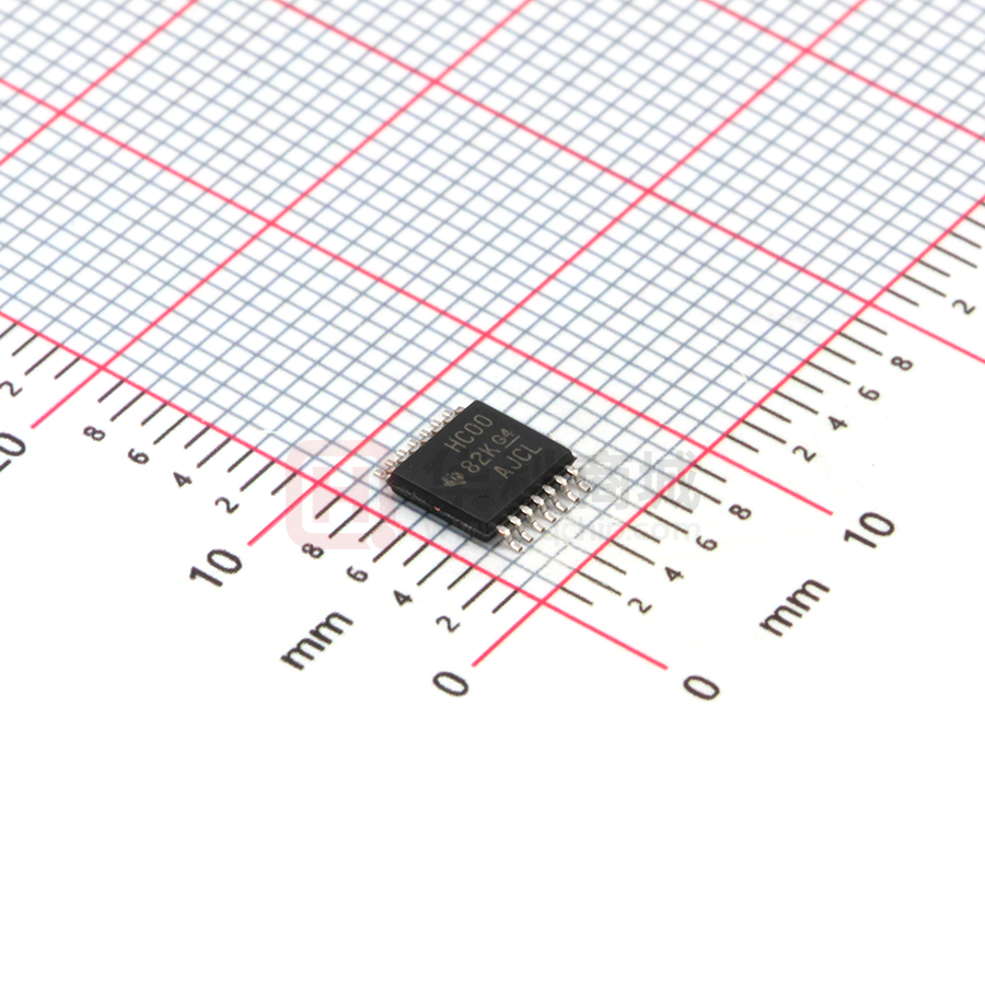
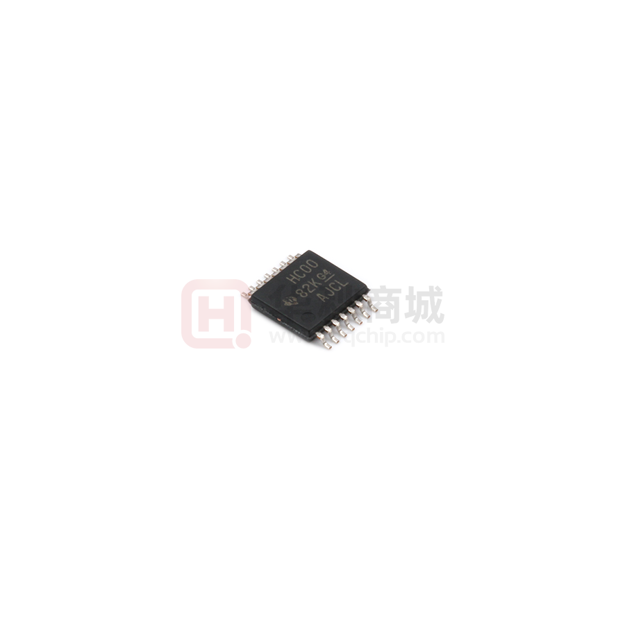
SN74HC00PW
TSSOP (14)
5.00 mm × 4.40 mm
•
•
•
•
•
AV Receivers
Portable Audio Docks
Blu-ray Players and Home Theater
MP3 Players or Recorders
Personal Digital Assistants (PDAs)
Power: Telecom or Server AC/DC Supply
(Single Controller: Analog and Digital)
Solid State Drives (SSDs): Client and Enterprise
TVs: LCD, Digital, and High-Definition (HDTV)
Tablets: Enterprise
Video Analytics: Server
Wireless Headsets, Keyboards, and Mice
SN54HC00
(1) For all available packages, see the orderable addendum at
the end of the data sheet.
Logic Diagram (Positive Logic)
A
B
Y
Copyright © 2016, Texas Instruments Incorporated
1
An IMPORTANT NOTICE at the end of this data sheet addresses availability, warranty, changes, use in safety-critical applications,
intellectual property matters and other important disclaimers. PRODUCTION DATA.
�SN54HC00, SN74HC00
SCLS181F – DECEMBER 1982 – REVISED JULY 2016
www.ti.com
Table of Contents
1
2
3
4
5
6
7
8
Features ..................................................................
Applications ...........................................................
Description .............................................................
Revision History.....................................................
Pin Configuration and Functions .........................
Specifications.........................................................
1
1
1
2
3
4
6.1
6.2
6.3
6.4
6.5
6.6
6.7
4
4
4
5
5
6
6
Absolute Maximum Ratings ......................................
ESD Ratings..............................................................
Recommended Operating Conditions.......................
Thermal Information ..................................................
Electrical Characteristics...........................................
Switching Characteristics ..........................................
Typical Characteristics ..............................................
Parameter Measurement Information .................. 7
Detailed Description .............................................. 8
8.1 Overview ................................................................... 8
8.2 Functional Block Diagram ......................................... 8
8.3 Feature Description................................................... 8
8.4 Device Functional Modes.......................................... 8
9
Application and Implementation .......................... 9
9.1 Application Information.............................................. 9
9.2 Typical Application .................................................... 9
10 Power Supply Recommendations ..................... 10
11 Layout................................................................... 10
11.1 Layout Guidelines ................................................ 10
11.2 Layout Example ................................................... 10
12 Device and Documentation Support ................. 11
12.1
12.2
12.3
12.4
12.5
12.6
12.7
Documentation Support ........................................
Related Links ........................................................
Receiving Notification of Documentation Updates
Community Resources..........................................
Trademarks ...........................................................
Electrostatic Discharge Caution ............................
Glossary ................................................................
11
11
11
11
11
11
11
13 Mechanical, Packaging, and Orderable
Information ........................................................... 11
4 Revision History
NOTE: Page numbers for previous revisions may differ from page numbers in the current version.
Changes from Revision E (August 2003) to Revision F
Page
•
Added Applications section, Device Information table, ESD Ratings table, Typical Characteristics section, Feature
Description section, Device Functional Modes, Application and Implementation section, Power Supply
Recommendations section, Layout section, Device and Documentation Support section, and Mechanical,
Packaging, and Orderable Information section ...................................................................................................................... 1
•
Added Military Disclaimer to Features list .............................................................................................................................. 1
•
Removed Ordering Information table; see POA at the end of data sheet.............................................................................. 1
•
Changed values in the Thermal Information table to align with JEDEC standards................................................................ 5
•
Deleted Operating Characteristics table; moved Cpd row to Electrical Characteristics......................................................... 5
2
Submit Documentation Feedback
Copyright © 1982–2016, Texas Instruments Incorporated
Product Folder Links: SN54HC00 SN74HC00
�SN54HC00, SN74HC00
www.ti.com
SCLS181F – DECEMBER 1982 – REVISED JULY 2016
5 Pin Configuration and Functions
D, DB, J, N, NS, PW, and W Package
14-Pin SOIC, SSOP, CDIP, PDIP, SOP, TSSOP, and CFP
Top View
10
3B
2Y
6
9
3A
GND
7
8
3Y
4B
5
19
2B
1Y
4
18
4A
NC
5
17
NC
2A
6
16
4Y
NC
7
15
NC
2B
8
14
3B
2Y
9
Not to scale
13
4Y
3A
11
VCC
4
20
2A
12
4A
3Y
12
NC
3
1
1Y
11
4B
NC
13
1A
2
2
1B
10
VCC
GND
14
1B
1
3
1A
FK Package
20-Pin LCCC
Top View
Not to scale
Pin Functions
PIN
SOIC, SSOP,
CDIP, PDIP, SOP,
TSSOP, CFP
LCCC
1A
1
2
I
Gate 1 input
1B
2
3
I
Gate 1 input
1Y
3
4
O
Gate 1 output
2A
4
6
I
Gate 2 input
2B
5
8
I
Gate 2 input
2Y
6
9
O
Gate 2 output
3A
9
13
I
Gate 3 input
3B
10
14
I
Gate 3 input
3Y
8
12
O
Gate 3 output
4A
12
18
I
Gate 4 input
4B
13
19
I
Gate 4 input
4Y
11
16
O
Gate 4 output
GND
7
10
—
Ground pin
NC
—
1, 5, 7,
11, 15,17
—
No internal connection
VCC
14
20
—
Power pin
NAME
I/O
DESCRIPTION
Copyright © 1982–2016, Texas Instruments Incorporated
Product Folder Links: SN54HC00 SN74HC00
Submit Documentation Feedback
3
�SN54HC00, SN74HC00
SCLS181F – DECEMBER 1982 – REVISED JULY 2016
www.ti.com
6 Specifications
6.1 Absolute Maximum Ratings
over operating free-air temperature range (unless otherwise noted) (1)
Supply voltage, VCC
Input clamp current, IIK (VI < 0 or VI > VCC)
MIN
MAX
UNIT
–0.5
7
V
(2)
±20
mA
Output clamp current, IOK (VO < 0 or VO > VCC) (2)
±20
mA
Continuous output current, IO (VO = 0 to VCC)
±25
mA
±50
mA
150
°C
Continuous current through VCC or GND
Storage temperature, Tstg
(1)
(2)
–65
Stresses beyond those listed under Absolute Maximum Ratings may cause permanent damage to the device. These are stress ratings
only, which do not imply functional operation of the device at these or any other conditions beyond those indicated under Recommended
Operating Conditions. Exposure to absolute-maximum-rated conditions for extended periods may affect device reliability.
The input and output voltage ratings may be exceeded if the input and output current ratings are observed.
6.2 ESD Ratings
VALUE
V(ESD)
(1)
(2)
Electrostatic discharge
Human-body model (HBM), per ANSI/ESDA/JEDEC JS-001 (1)
±2000
Charged-device model (CDM), per JEDEC specification JESD22-C101 (2)
±1000
UNIT
V
JEDEC document JEP155 states that 500-V HBM allows safe manufacturing with a standard ESD control process.
JEDEC document JEP157 states that 250-V CDM allows safe manufacturing with a standard ESD control process.
6.3 Recommended Operating Conditions
over operating free-air temperature range (unless otherwise noted) (1)
VCC
Supply voltage
VCC = 2 V
VIH
High-level input voltage
MIN
NOM
MAX
2
5
6
UNIT
V
1.5
VCC = 4.5 V
3.15
VCC = 6 V
V
4.2
VCC = 2 V
0.5
VIL
Low-level input voltage
VCC = 4.5 V
1.35
VI
Input voltage
0
VCC
V
VO
Output voltage
0
VCC
V
∆t/∆v
Input transition rise and fall time
VCC = 6 V
1.8
VCC = 2 V
TA
(1)
4
Operating free-air temperature
V
1000
VCC = 4.5 V
500
VCC = 6 V
400
SN54HC00
–55
125
SN74HC00
–40
85
ns
°C
All unused inputs of the device must be held at VCC or GND to ensure proper device operation. Refer to Implications of Slow or Floating
CMOS Inputs application report.
Submit Documentation Feedback
Copyright © 1982–2016, Texas Instruments Incorporated
Product Folder Links: SN54HC00 SN74HC00
�SN54HC00, SN74HC00
www.ti.com
SCLS181F – DECEMBER 1982 – REVISED JULY 2016
6.4 Thermal Information
SN74HC00
THERMAL METRIC (1)
D (SOIC)
DB (SSOP)
N (PDIP)
NS (SOP)
PW (TSSOP)
14 PINS
14 PINS
14 PINS
14 PINS
14 PINS
UNIT
RθJA
Junction-to-ambient thermal
resistance
94.7
108.3
57.5
91
122.9
°C/W
RθJC(top)
Junction-to-case (top) thermal
resistance
54.6
60.3
45.1
48.8
51.5
°C/W
RθJB
Junction-to-board thermal
resistance
49
55.7
37.3
49.8
64.6
°C/W
ψJT
Junction-to-top characterization
parameter
21.1
25
30.3
18.4
6.6
°C/W
ψJB
Junction-to-board
characterization parameter
48.7
55.2
37.2
49.5
64
°C/W
(1)
For more information about traditional and new thermal metrics, see the Semiconductor and IC Package Thermal Metrics application
report.
6.5 Electrical Characteristics
over recommended operating free-air temperature range (unless otherwise noted)
PARAMETER
TEST CONDITIONS
IOH = –20 µA
VOH
VI = VIH or VIL
IOH = –4 mA, VCC = 4.5 V
IOH = –5.2 mA, VCC = 6 V
IOL = 20 µA
VOL
VI = VIH or VIL
IOL = 4 mA, VCC = 4.5 V
MIN
TYP
VCC = 2 V
1.9
1.998
VCC = 4.5 V
4.4
4.499
VCC = 6 V
5.9
5.999
TA = 25°C
3.98
4.3
SN54HC00
3.7
SN74HC00
3.84
TA = 25°C
5.48
SN54HC00
5.2
SN74HC00
5.34
II
VI = VCC or 0, VCC = 6 V
ICC
VI = VCC or 0, IO = 0,
VCC = 6 V
Ci
0.002
0.1
0.001
0.1
VCC = 6 V
0.001
0.1
TA = 25°C
0.17
0.26
SN54HC00
0.4
SN74HC00
0.33
Cpd
0.15
0.4
SN74HC00
0.33
±0.1
SNx4HC00
±100
±1000
TA = 25°C
2
SN54HC00
40
SN74HC00
20
3
No load, TA = 25°C
10
20
Copyright © 1982–2016, Texas Instruments Incorporated
Product Folder Links: SN54HC00 SN74HC00
V
0.26
SN54HC00
VCC = 2 V to 6 V
Power
dissipation
capacitance
per gate
5.8
VCC = 4.5 V
TA = 25°C
UNIT
V
VCC = 2 V
TA = 25°C
IOL = 5.2 mA, VCC = 6 V
MAX
Submit Documentation Feedback
nA
µA
pF
pF
5
�SN54HC00, SN74HC00
SCLS181F – DECEMBER 1982 – REVISED JULY 2016
www.ti.com
6.6 Switching Characteristics
over recommended operating free-air temperature range, CL= 50 pF, see Figure 2 (unless otherwise noted)
PARAMETER
TEST CONDITIONS
MIN
TA = 25°C
VCC = 2 V
TYP
45
SN54HC00
VCC = 4.5 V
9
27
SN74HC00
23
8
SN54HC00
38
SN54HC00
95
TA = 25°C
VCC = 4.5 V
8
SN54HC00
15
22
SN74HC00
ns
19
TA = 25°C
VCC = 6 V
75
110
SN74HC00
To Y (output)
15
20
TA = 25°C
tt
ns
23
SN74HC00
VCC = 2 V
18
SN54HC00
TA = 25°C
VCC = 6 V
90
115
TA = 25°C
From A or B (input) to Y (output)
UNIT
135
SN74HC00
tpd
MAX
6
13
SN54HC00
19
SN74HC00
16
6.7 Typical Characteristics
50
45
40
tpd (ns)
35
30
25
20
15
10
5
CL=50pF
0
2.0
2.5
3.0
3.5
4.0
4.5
5.0
5.5
VCC (V)
6.0
C001
Figure 1. Propagation Delay vs VCC
6
Submit Documentation Feedback
Copyright © 1982–2016, Texas Instruments Incorporated
Product Folder Links: SN54HC00 SN74HC00
�SN54HC00, SN74HC00
www.ti.com
SCLS181F – DECEMBER 1982 – REVISED JULY 2016
7 Parameter Measurement Information
From Output
Under Test
Test
Point
Input
VCC
50%
50%
0V
CL = 50 pF
(see Note A)
tPLH
In-Phase
Output
LOAD CIRCUIT
tPHL
90%
50%
10%
90%
tr
Input
90%
50%
10%
90%
tPHL
VCC
50%
10% 0 V
tr
Out-of-Phase
Output
tPLH
90%
50%
10%
tf
50%
10%
90%
tf
VOH
VOL
tr
VOLTAGE WAVEFORMS
PROPAGATION DELAY AND OUTPUT TRANSITION TIMES
VOLTAGE WAVEFORM
INPUT RISE AND FALL TIMES
NOTES: A.
VOH
50%
10%
VOL
tf
CL includes probe and test-fixture capacitance.
B.
Phase relationships between waveforms were chosen arbitrarily. All input pulses are supplied by
generators having the following characteristics: PRR ≤ 1 MHz, ZO = 50 Ω, tr = 6 ns, tf = 6 ns.
C.
The outputs are measured one at a time with one input transition per measurement.
D.
tPLH and tPHL are the same as tpd.
Figure 2. Load Circuit and Voltage Waveforms
Copyright © 1982–2016, Texas Instruments Incorporated
Product Folder Links: SN54HC00 SN74HC00
Submit Documentation Feedback
7
�SN54HC00, SN74HC00
SCLS181F – DECEMBER 1982 – REVISED JULY 2016
www.ti.com
8 Detailed Description
8.1 Overview
The SNx4HC00 devices perform the NAND Boolean function Y = A × B or Y = A + B in positive logic. The
devices have a wide operating range of VCC from 2 V to 6 V.
8.2 Functional Block Diagram
A
Y
B
Copyright © 2016, Texas Instruments Incorporated
8.3 Feature Description
The SNx4HC00 devices have a wide operating voltage range that operates from 2 V to 6 V. They allow inputs
and outputs up to VCC. The devices can drive outputs at 4 mA at 5-V VCC.
8.4 Device Functional Modes
Table 1 lists the functional modes for the SNx4HC00.
Table 1. Function Table
INPUTS
8
Submit Documentation Feedback
OUTPUT
A
B
Y
H
H
L
L
X
H
X
L
H
Copyright © 1982–2016, Texas Instruments Incorporated
Product Folder Links: SN54HC00 SN74HC00
�SN54HC00, SN74HC00
www.ti.com
SCLS181F – DECEMBER 1982 – REVISED JULY 2016
9 Application and Implementation
NOTE
Information in the following applications sections is not part of the TI component
specification, and TI does not warrant its accuracy or completeness. TI’s customers are
responsible for determining suitability of components for their purposes. Customers should
validate and test their design implementation to confirm system functionality.
9.1 Application Information
The SNx4HC00 is a low-power, wide-operating-voltage NAND gate. This device can drive up to 10 LSTTL loads
and can drive 4-mA outputs at 5-V VCC.
9.2 Typical Application
S
Q
Q
R
Copyright © 2016,
Texas Instruments Incorporated
Figure 3. Typical NAND Gate Application and Supply Voltage
9.2.1 Design Requirements
The SNx4HC00 devices use CMOS technology and have balanced output drive. Take care to avoid bus
contention because it drives currents that would exceed maximum limits. The high drive also creates fast edges
into light loads. Routing and load conditions must be considered to prevent ringing.
9.2.2 Detailed Design Procedure
• Recommended input conditions:
– Specified high and low levels. See VIH and VIL in Recommended Operating Conditions.
• Recommended output conditions:
– Load currents must not exceed 25 mA per output and 50 mA total for the part.
– Outputs must not be pulled above VCC.
9.2.3 Application Curve
40
35
30
tt (ns)
25
20
15
10
5
CL=50pF
0
2.0
2.5
3.0
3.5
4.0
4.5
5.0
5.5
VCC (V)
6.0
C002
Figure 4. Transition Time vs VCC
Copyright © 1982–2016, Texas Instruments Incorporated
Product Folder Links: SN54HC00 SN74HC00
Submit Documentation Feedback
9
�SN54HC00, SN74HC00
SCLS181F – DECEMBER 1982 – REVISED JULY 2016
www.ti.com
10 Power Supply Recommendations
The power supply can be any voltage between the MIN and MAX supply voltage rating located in Recommended
Operating Conditions.
Each VCC pin must have a good bypass capacitor to prevent power disturbance. For devices with a single supply,
TI recommends a 0.1-µF bypass capacitor; if there are multiple VCC pins, then TI recommends 0.01-µF or
0.022-µF bypass capacitors for each power pin. It is acceptable to parallel multiple bypass capacitors to reject
different frequencies of noise. A 0.1 µF and a 1 µF are commonly used in parallel. The bypass capacitor must be
installed as close to the power pin as possible for best results.
11 Layout
11.1 Layout Guidelines
When using multiple bit logic devices inputs must never float.
In many cases, functions or parts of functions of digital logic devices are unused, for example, when only two
inputs of a triple-input and gate are used or only 3 of the 4 buffer gates are used. Such input pins must not be left
unconnected because the undefined voltages at the outside connections result in undefined operational states.
Figure 5 specifies the rules that must be observed under all circumstances. All unused inputs of digital logic
devices must be connected to a high or low bias to prevent them from floating. The logic level that must be
applied to any particular unused input depends on the function of the device. Generally they are tied to GND or
VCC, whichever makes more sense or is more convenient. It is generally acceptable to float outputs, unless the
part is a transceiver.
11.2 Layout Example
Vcc
Unused Input
Input
Output
Output
Unused Input
Input
Figure 5. Layout Diagram
10
Submit Documentation Feedback
Copyright © 1982–2016, Texas Instruments Incorporated
Product Folder Links: SN54HC00 SN74HC00
�SN54HC00, SN74HC00
www.ti.com
SCLS181F – DECEMBER 1982 – REVISED JULY 2016
12 Device and Documentation Support
12.1 Documentation Support
12.1.1 Related Documentation
For related documentation see the following:
Implications of Slow or Floating CMOS Inputs (SCBA004)
12.2 Related Links
The table below lists quick access links. Categories include technical documents, support and community
resources, tools and software, and quick access to sample or buy.
Table 2. Related Links
PARTS
PRODUCT FOLDER
SAMPLE & BUY
TECHNICAL
DOCUMENTS
TOOLS &
SOFTWARE
SUPPORT &
COMMUNITY
SN54HC00
Click here
Click here
Click here
Click here
Click here
SN74HC00
Click here
Click here
Click here
Click here
Click here
12.3 Receiving Notification of Documentation Updates
To receive notification of documentation updates, navigate to the device product folder on ti.com. In the upper
right corner, click on Alert me to register and receive a weekly digest of any product information that has
changed. For change details, review the revision history included in any revised document.
12.4 Community Resources
The following links connect to TI community resources. Linked contents are provided "AS IS" by the respective
contributors. They do not constitute TI specifications and do not necessarily reflect TI's views; see TI's Terms of
Use.
TI E2E™ Online Community TI's Engineer-to-Engineer (E2E) Community. Created to foster collaboration
among engineers. At e2e.ti.com, you can ask questions, share knowledge, explore ideas and help
solve problems with fellow engineers.
Design Support TI's Design Support Quickly find helpful E2E forums along with design support tools and
contact information for technical support.
12.5 Trademarks
E2E is a trademark of Texas Instruments.
All other trademarks are the property of their respective owners.
12.6 Electrostatic Discharge Caution
These devices have limited built-in ESD protection. The leads should be shorted together or the device placed in conductive foam
during storage or handling to prevent electrostatic damage to the MOS gates.
12.7 Glossary
SLYZ022 — TI Glossary.
This glossary lists and explains terms, acronyms, and definitions.
13 Mechanical, Packaging, and Orderable Information
The following pages include mechanical, packaging, and orderable information. This information is the most
current data available for the designated devices. This data is subject to change without notice and revision of
this document. For browser-based versions of this data sheet, refer to the left-hand navigation.
Copyright © 1982–2016, Texas Instruments Incorporated
Product Folder Links: SN54HC00 SN74HC00
Submit Documentation Feedback
11
�PACKAGE OPTION ADDENDUM
www.ti.com
24-Aug-2018
PACKAGING INFORMATION
Orderable Device
Status
(1)
Package Type Package Pins Package
Drawing
Qty
Eco Plan
Lead/Ball Finish
MSL Peak Temp
(2)
(6)
(3)
Op Temp (°C)
Device Marking
(4/5)
5962-8403701VCA
ACTIVE
CDIP
J
14
1
TBD
A42
N / A for Pkg Type
-55 to 125
5962-8403701VC
A
SNV54HC00J
5962-8403701VDA
ACTIVE
CFP
W
14
1
TBD
A42
N / A for Pkg Type
-55 to 125
5962-8403701VD
A
SNV54HC00W
84037012A
ACTIVE
LCCC
FK
20
1
TBD
POST-PLATE
N / A for Pkg Type
-55 to 125
84037012A
SNJ54HC
00FK
8403701CA
ACTIVE
CDIP
J
14
1
TBD
A42
N / A for Pkg Type
-55 to 125
8403701CA
SNJ54HC00J
8403701DA
ACTIVE
CFP
W
14
1
TBD
A42
N / A for Pkg Type
-55 to 125
8403701DA
SNJ54HC00W
JM38510/65001B2A
ACTIVE
LCCC
FK
20
1
TBD
POST-PLATE
N / A for Pkg Type
-55 to 125
JM38510/
65001B2A
JM38510/65001BCA
ACTIVE
CDIP
J
14
1
TBD
A42
N / A for Pkg Type
-55 to 125
JM38510/
65001BCA
JM38510/65001BDA
ACTIVE
CFP
W
14
1
TBD
A42
N / A for Pkg Type
-55 to 125
JM38510/
65001BDA
M38510/65001B2A
ACTIVE
LCCC
FK
20
1
TBD
POST-PLATE
N / A for Pkg Type
-55 to 125
JM38510/
65001B2A
M38510/65001BCA
ACTIVE
CDIP
J
14
1
TBD
A42
N / A for Pkg Type
-55 to 125
JM38510/
65001BCA
M38510/65001BDA
ACTIVE
CFP
W
14
1
TBD
A42
N / A for Pkg Type
-55 to 125
JM38510/
65001BDA
SN54HC00J
ACTIVE
CDIP
J
14
1
TBD
A42
N / A for Pkg Type
-55 to 125
SN54HC00J
SN74HC00D
ACTIVE
SOIC
D
14
50
Green (RoHS
& no Sb/Br)
CU NIPDAU
Level-1-260C-UNLIM
-40 to 85
HC00
SN74HC00DBR
ACTIVE
SSOP
DB
14
2000
Green (RoHS
& no Sb/Br)
CU NIPDAU
Level-1-260C-UNLIM
-40 to 85
HC00
SN74HC00DE4
ACTIVE
SOIC
D
14
50
Green (RoHS
& no Sb/Br)
CU NIPDAU
Level-1-260C-UNLIM
-40 to 85
HC00
SN74HC00DG4
ACTIVE
SOIC
D
14
50
Green (RoHS
& no Sb/Br)
CU NIPDAU
Level-1-260C-UNLIM
-40 to 85
HC00
Addendum-Page 1
Samples
�PACKAGE OPTION ADDENDUM
www.ti.com
24-Aug-2018
Orderable Device
Status
(1)
Package Type Package Pins Package
Drawing
Qty
Eco Plan
Lead/Ball Finish
MSL Peak Temp
(2)
(6)
(3)
Op Temp (°C)
Device Marking
(4/5)
SN74HC00DR
ACTIVE
SOIC
D
14
2500
Green (RoHS
& no Sb/Br)
CU NIPDAU | CU SN
Level-1-260C-UNLIM
-40 to 85
HC00
SN74HC00DRE4
ACTIVE
SOIC
D
14
2500
Green (RoHS
& no Sb/Br)
CU NIPDAU
Level-1-260C-UNLIM
-40 to 85
HC00
SN74HC00DRG4
ACTIVE
SOIC
D
14
2500
Green (RoHS
& no Sb/Br)
CU NIPDAU
Level-1-260C-UNLIM
-40 to 85
HC00
SN74HC00DT
ACTIVE
SOIC
D
14
250
Green (RoHS
& no Sb/Br)
CU NIPDAU
Level-1-260C-UNLIM
-40 to 85
HC00
SN74HC00DTE4
ACTIVE
SOIC
D
14
250
Green (RoHS
& no Sb/Br)
CU NIPDAU
Level-1-260C-UNLIM
-40 to 85
HC00
SN74HC00DTG4
ACTIVE
SOIC
D
14
250
Green (RoHS
& no Sb/Br)
CU NIPDAU
Level-1-260C-UNLIM
-40 to 85
HC00
SN74HC00N
ACTIVE
PDIP
N
14
25
Green (RoHS
& no Sb/Br)
CU NIPDAU | CU SN
N / A for Pkg Type
-40 to 85
SN74HC00N
SN74HC00NE4
ACTIVE
PDIP
N
14
25
Green (RoHS
& no Sb/Br)
CU NIPDAU
N / A for Pkg Type
-40 to 85
SN74HC00N
SN74HC00NSR
ACTIVE
SO
NS
14
2000
Green (RoHS
& no Sb/Br)
CU NIPDAU
Level-1-260C-UNLIM
-40 to 85
HC00
SN74HC00PW
ACTIVE
TSSOP
PW
14
90
Green (RoHS
& no Sb/Br)
CU NIPDAU
Level-1-260C-UNLIM
-40 to 85
HC00
SN74HC00PWR
ACTIVE
TSSOP
PW
14
2000
Green (RoHS
& no Sb/Br)
CU NIPDAU | CU SN
Level-1-260C-UNLIM
-40 to 85
HC00
SN74HC00PWRG4
ACTIVE
TSSOP
PW
14
2000
Green (RoHS
& no Sb/Br)
CU NIPDAU
Level-1-260C-UNLIM
-40 to 85
HC00
SN74HC00PWT
ACTIVE
TSSOP
PW
14
250
Green (RoHS
& no Sb/Br)
CU NIPDAU
Level-1-260C-UNLIM
-40 to 85
HC00
SNJ54HC00FK
ACTIVE
LCCC
FK
20
1
TBD
POST-PLATE
N / A for Pkg Type
-55 to 125
84037012A
SNJ54HC
00FK
SNJ54HC00J
ACTIVE
CDIP
J
14
1
TBD
A42
N / A for Pkg Type
-55 to 125
8403701CA
SNJ54HC00J
SNJ54HC00W
ACTIVE
CFP
W
14
1
TBD
A42
N / A for Pkg Type
-55 to 125
8403701DA
SNJ54HC00W
(1)
The marketing status values are defined as follows:
ACTIVE: Product device recommended for new designs.
LIFEBUY: TI has announced that the device will be discontinued, and a lifetime-buy period is in effect.
Addendum-Page 2
Samples
�PACKAGE OPTION ADDENDUM
www.ti.com
24-Aug-2018
NRND: Not recommended for new designs. Device is in production to support existing customers, but TI does not recommend using this part in a new design.
PREVIEW: Device has been announced but is not in production. Samples may or may not be available.
OBSOLETE: TI has discontinued the production of the device.
(2)
RoHS: TI defines "RoHS" to mean semiconductor products that are compliant with the current EU RoHS requirements for all 10 RoHS substances, including the requirement that RoHS substance
do not exceed 0.1% by weight in homogeneous materials. Where designed to be soldered at high temperatures, "RoHS" products are suitable for use in specified lead-free processes. TI may
reference these types of products as "Pb-Free".
RoHS Exempt: TI defines "RoHS Exempt" to mean products that contain lead but are compliant with EU RoHS pursuant to a specific EU RoHS exemption.
Green: TI defines "Green" to mean the content of Chlorine (Cl) and Bromine (Br) based flame retardants meet JS709B low halogen requirements of


 工商网监
湘ICP备2023018690号
工商网监
湘ICP备2023018690号