Sample &
Buy
Product
Folder
Support &
Community
Tools &
Software
Technical
Documents
SN54HC164, SN74HC164
SCLS115G – DECEMBER 1982 – REVISED SEPTEMBER 2015
SNx4HC164 8-Bit Parallel-Out Serial Shift Registers
1 Features
3 Description
•
•
•
•
•
•
•
•
•
•
These 8-bit shift registers feature AND-gated serial
inputs and an asynchronous clear (CLR) input. The
gated serial (A and B) inputs permit complete control
over incoming data; a low at either input inhibits entry
of the new data and resets the first flip-flop to the low
level at the next clock (CLK) pulse. A high-level input
enables the other input, which then determines the
state of the first flip-flop. Data at the serial inputs can
be changed while CLK is high or low, provided the
minimum set-up time requirements are met. Clocking
occurs on the low-to-high-level transition of CLK.
1
Wide Operating Voltage Range of 2 V to 6 V
Outputs Can Drive Up to 10 LSTTL Loads
Low Power Consumption, 80-μA Maximum ICC
Typical tpd = 20 ns
±4-mA Output Drive at 5 V
Low Input Current of 1-μA Maximum
AND-Gated (Enable/Disable) Serial Inputs
Fully Buffered Clock and Serial Inputs
Direct Clear
On Products Compliant to MIL-PRF-38535,
All Parameters Are Tested Unless Otherwise
Noted. On All Other Products, Production
Processing Does Not Necessarily Include Testing
of All Parameters.
Device Information(1)
PART NUMBER
PACKAGE
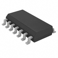
SN74HC164
2 Applications
•
•
•
•
Programable Logic Controllers
Appliances
Video Display Systems
Output Expander
SN54HC164
BODY SIZE (NOM)
SOIC (14)
8.65 mm × 3.91 mm
PDIP (14)
19.30 mm × 6.35 mm
SO (14)
10.30 mm × 5.30 mm
TSSOP (14)
5.00 mm × 4.40 mm
CDIP (14)
19.94 mm × 6.92 mm
CFP (14)
9.21 mm × 6.29 mm
LCCC (14)
9.39 mm × 9.39 mm
(1) For all available packages, see the orderable addendum at
the end of the data sheet.
Logic Diagram (Positive Logic)
CLK
A
B
CLR
8
1
2
C1
1D
R
C1
1D
R
C1
1D
R
C1
1D
R
C1
1D
R
C1
1D
R
C1
1D
R
C1
1D
R
9
3
QA
4
QB
5
QC
6
QD
10
QE
11
QF
12
QG
13
QH
Pin numbers shown are for the D, J, N, NS, PW, and W packages.
1
An IMPORTANT NOTICE at the end of this data sheet addresses availability, warranty, changes, use in safety-critical applications,
intellectual property matters and other important disclaimers. PRODUCTION DATA.
�SN54HC164, SN74HC164
SCLS115G – DECEMBER 1982 – REVISED SEPTEMBER 2015
www.ti.com
Table of Contents
1
2
3
4
5
6
7
Features ..................................................................
Applications ...........................................................
Description .............................................................
Revision History.....................................................
Device Comparison Table.....................................
Pin Configuration and Functions .........................
Specifications.........................................................
7.1
7.2
7.3
7.4
7.5
7.6
7.7
7.8
7.9
7.10
7.11
7.12
7.13
7.14
1
1
1
2
3
4
6
Absolute Maximum Ratings ...................................... 6
ESD Ratings ............................................................ 6
Recommended Operating Conditions....................... 6
Thermal Information .................................................. 7
Electrical Characteristics, TA = 25°C ........................ 7
Electrical Characteristics, TA = –55°C to 125°C ....... 7
Electrical Characteristics, TA = –55°C to 85°C ......... 8
Timing Requirements, TA = 25°C.............................. 8
Timing Requirements, TA = –55°C to 125°C ............ 9
Timing Requirements, TA = –55°C to 85°C ............ 9
Switching Characteristics, TA = 25°C.................... 10
Switching Characteristics, TA = –55°C to 125°C .. 10
Switching Characteristics, TA = –55°C to 85°C .... 11
Typical Characteristics .......................................... 12
8
9
Parameter Measurement Information ................ 13
Detailed Description ............................................ 14
9.1
9.2
9.3
9.4
Overview .................................................................
Functional Block Diagram .......................................
Feature Description.................................................
Device Functional Modes........................................
14
14
14
14
10 Application and Implementation........................ 15
10.1 Application Information.......................................... 15
10.2 Typical Application ............................................... 15
11 Power Supply Recommendations ..................... 17
12 Layout................................................................... 17
12.1 Layout Guidelines ................................................. 17
12.2 Layout Example .................................................... 17
13 Device and Documentation Support ................. 18
13.1
13.2
13.3
13.4
13.5
13.6
Documentation Support ........................................
Related Links ........................................................
Community Resources..........................................
Trademarks ...........................................................
Electrostatic Discharge Caution ............................
Glossary ................................................................
18
18
18
18
18
18
14 Mechanical, Packaging, and Orderable
Information ........................................................... 18
4 Revision History
NOTE: Page numbers for previous revisions may differ from page numbers in the current version.
Changes from Revision F (October 2013) to Revision G
Page
•
Added Applications section, Device Information table, Pin Configuration and Functions section, ESD Ratings table,
Thermal Information table, Typical Characteristics section, Feature Description section, Device Functional Modes,
Application and Implementation section, Power Supply Recommendations section, Layout section, Device and
Documentation Support section, and Mechanical, Packaging, and Orderable Information section....................................... 1
•
Added Military Disclaimer to Features list. ............................................................................................................................. 1
•
Added Handling Ratings table. ............................................................................................................................................... 6
Changes from Revision E (November 2010) to Revision F
Page
•
Updated document to new TI data sheet format. ................................................................................................................... 1
•
Removed Ordering Information table. .................................................................................................................................... 1
•
Updated operating temperature range. .................................................................................................................................. 6
2
Submit Documentation Feedback
Copyright © 1982–2015, Texas Instruments Incorporated
Product Folder Links: SN54HC164 SN74HC164
�SN54HC164, SN74HC164
www.ti.com
SCLS115G – DECEMBER 1982 – REVISED SEPTEMBER 2015
5 Device Comparison Table
PART NUMBER
PACKAGE
BODY SIZE (NOM)
SN74HC164D
SOIC (14)
8.65 mm × 3.91 mm
SN74HC164N
PDIP (14)
19.30 mm × 6.35 mm
SN74HC164NS
SO (14)
10.30 mm × 5.30 mm
SN74HC164PW
TSSOP (14)
5.00 mm × 4.40 mm
SN54HC164J
CDIP (14)
19.94 mm × 6.92 mm
SN54HC164W
CFP (14)
9.21 mm × 6.29 mm
SN54HC164FK
LCCC (14)
9.39 mm × 9.39 mm
Copyright © 1982–2015, Texas Instruments Incorporated
Product Folder Links: SN54HC164 SN74HC164
Submit Documentation Feedback
3
�SN54HC164, SN74HC164
SCLS115G – DECEMBER 1982 – REVISED SEPTEMBER 2015
www.ti.com
6 Pin Configuration and Functions
D, N, NS, J, W, or PW Package
14-Pin SOIC, PDIP, SO, CDIP, CFP, or TSSOP
Top View
A
B
QA
QB
QC
QD
GND
1
14
2
13
3
12
4
11
5
10
6
9
7
8
VCC
QH
QG
QF
QE
CLR
CLK
Pin Functions
PIN
SOIC, PDIP, SO,
CDIP, CFP, or
TSSOP NO.
NAME
I/O
DESCRIPTION
1
A
I
Gated Serial Input 1
2
B
I
Gated Serial Input 2
3
QA
O
Parallel Output
4
QB
O
Parallel Output
5
QC
O
Parallel Output
6
QD
O
Parallel Output
7
GND
-
Ground
8
CLK
I
Clock
9
CLR
I
Clear 1 Active-Low
10
QE
O
Parallel Output
11
QF
O
Parallel Output
12
QG
O
Parallel Output
13
QH
O
Parallel Output
14
VCC
—
Power
4
Submit Documentation Feedback
Copyright © 1982–2015, Texas Instruments Incorporated
Product Folder Links: SN54HC164 SN74HC164
�SN54HC164, SN74HC164
www.ti.com
SCLS115G – DECEMBER 1982 – REVISED SEPTEMBER 2015
B
A
NC
VCC
QH
FK Package
20-Pin LCCC
Top View
4
3 2 1 20 19
18
5
17
6
16
7
15
8
14
9 10 11 12 13
QG
NC
QF
NC
QE
QD
GND
NC
CLK
CLR
QA
NC
QB
NC
QC
NC – No internal connection
Pin Functions
PIN
LCCC NO.
NAME
I/O
DESCRIPTION
1
NC
—
2
A
I
No Connect
Gated Serial Input 1
3
B
I
Gated Serial Input 2
4
QA
O
Parallel Output
5
NC
—
No Connect
6
QB
O
Parallel Output
7
NC
—
No Connect
8
QC
O
Parallel Output
9
QD
O
Parallel Output
10
GND
—
Ground
11
NC
—
No Connect
12
CLK
I
Clock
13
CLR
I
Clear 1 Active-Low
14
QE
O
Parallel Output
15
NC
—
No Connect
16
QF
O
Parallel Output
17
NC
—
No Connect
18
QG
O
Parallel Output
19
QH
O
Parallel Output
20
VCC
—
Power
Copyright © 1982–2015, Texas Instruments Incorporated
Product Folder Links: SN54HC164 SN74HC164
Submit Documentation Feedback
5
�SN54HC164, SN74HC164
SCLS115G – DECEMBER 1982 – REVISED SEPTEMBER 2015
www.ti.com
7 Specifications
7.1 Absolute Maximum Ratings
over operating free-air temperature range (unless otherwise noted) (1)
VCC
Supply voltage
(2)
MIN
MAX
UNITS
−0.5
7
V
IIK
Input clamp current
VI < 0 or VI > VCC
±20
mA
IOK
Output clamp current (2)
VO < 0 or VO > VCC
±20
mA
IO
Continuous output current
VO = 0 to VCC
±25
mA
±50
mA
150
°C
Continuous current through VCC or GND
Tstg
(1)
(2)
Storage temperature
–65
Stresses beyond those listed under Absolute Maximum Ratings may cause permanent damage to the device. These are stress ratings
only, and functional operation of the device at these or any other conditions beyond those indicated under Recommended Operating
Conditions is not implied. Exposure to absolute-maximum-rated conditions for extended periods may affect device reliability.
The input and output voltage ratings may be exceeded if the input and output current ratings are observed.
7.2 ESD Ratings
VALUE
V(ESD)
(1)
(2)
Electrostatic discharge
Human body model (HBM), per ANSI/ESDA/JEDEC JS-001 (1)
±2000
Charged-device model (CDM), per JEDEC specification JESD22-C101 (2)
±1000
UNIT
V
JEDEC document JEP155 states that 500-V HBM allows safe manufacturing with a standard ESD control process.
JEDEC document JEP157 states that 250-V CDM allows safe manufacturing with a standard ESD control process.
7.3 Recommended Operating Conditions
over operating free-air temperature range (unless otherwise noted) (1)
SN54HC164
VCC
Supply voltage
VCC = 2 V
VIH
High-level input voltage
VCC = 4.5 V
VCC = 6 V
NOM
MAX
2
5
6
Low-level input voltage
Input voltage
VO
Output voltage
TA
(1)
(2)
6
Input transition rise and fall
time
Operating free-air temperature
MAX
2
5
6
3.15
3.15
4.2
4.2
VCC = 4.5 V
0
0
VCC = 2 V
Δt/Δv (2)
NOM
1.5
VCC = 6 V
VI
MIN
1.5
VCC = 2 V
VIL
SN74HC164
MIN
0.5
1.35
1.35
1.8
1.8
0
VCC
0
V
VCC
V
1000
VCC = 4.5 V
500
500
VCC = 6 V
400
400
125
–40
V
VCC
1000
–55
V
V
0.5
VCC
UNIT
125
ns
°C
All unused inputs of the device must be held at VCC or GND to ensure proper device operation. Refer to the TI application report,
Implications of Slow or Floating CMOS Inputs, SCBA004.
If this device is used in the threshold region (from VIL max = 0.5 V to VIH min = 1.5 V), there is a potential to go into the wrong state from
induced grounding, causing double clocking. Operating with the inputs at tt = 1000 ns and VCC = 2 V does not damage the device;
however, functionally, the CLK inputs are not ensured while in the shift, count, or toggle operating modes.
Submit Documentation Feedback
Copyright © 1982–2015, Texas Instruments Incorporated
Product Folder Links: SN54HC164 SN74HC164
�SN54HC164, SN74HC164
www.ti.com
SCLS115G – DECEMBER 1982 – REVISED SEPTEMBER 2015
7.4 Thermal Information
SN54HC164
THERMAL METRIC (1)
RθJA
(1)
SN74HC164
J
(CDIP)
W
(CFP)
FK
(LCCC)
D
(SOIC)
N
(PDIP)
NS
(SO)
PW
(TSSOP)
14
PINS
14
PINS
20
PINS
14
PINS
14
PINS
14
PINS
14
PINS
—
—
—
86
80
76
113
Junction-to-ambient thermal
resistance
UNIT
°C/W
For more information about traditional and new thermal metrics, see the Semiconductor and IC Package Thermal Metrics application
report, SPRA953.
7.5 Electrical Characteristics, TA = 25°C
over recommended operating free-air temperature range (unless otherwise noted)
PARAMETER
TEST CONDITIONS
IOH = –20 μA
VOH
VI = VIH or VIL
IOH = –4 mA
IOH = –5.2 mA
IOL = 20 μA
VOL
VI = VIH or VIL
IOL = 4 mA
IOL = 5.2 mA
II
VI = VCC or 0
ICC
VI = VCC or 0
IO = 0
VCC
MIN
TYP
2V
1.9
1.998
4.5 V
4.4
4.499
6V
5.9
5.999
4.5 V
3.98
4.3
6V
5.48
MAX
V
5.8
2V
0.002
0.1
4.5 V
0.001
0.1
6V
0.001
0.1
4.5 V
0.17
0.26
6V
0.15
0.26
6V
±0.1
±100
nA
8
µA
10
pF
6V
2 V to
6V
Ci
UNIT
3
V
7.6 Electrical Characteristics, TA = –55°C to 125°C
over recommended operating free-air temperature range (unless otherwise noted)
PARAMETER
TEST CONDITIONS
MIN
IOH = –20 μA
VOH
VI = VIH or VIL
IOH = –4 mA
IOH = –5.2 mA
IOL = 20 μA
VOL
VI = VIH or VIL
IOL = 4 mA
IOL = 5.2 mA
II
VI = VCC or 0
ICC
VI = VCC or 0
IO = 0
Ci
Recommended
SN74HC164
SN54HC164
VCC
TYP
MAX
MIN
2V
1.9
1.9
4.5 V
4.4
4.4
6V
5.9
5.9
4.5 V
3.7
3.7
6V
5.2
TYP
UNIT
MAX
V
5.2
2V
0.1
0.1
4.5 V
0.1
0.1
6V
0.1
0.1
4.5 V
0.4
0.4
6V
0.4
0.4
6V
±1000
±1000
nA
6V
160
160
µA
2 V to
6V
10
10
pF
Copyright © 1982–2015, Texas Instruments Incorporated
Product Folder Links: SN54HC164 SN74HC164
Submit Documentation Feedback
V
7
�SN54HC164, SN74HC164
SCLS115G – DECEMBER 1982 – REVISED SEPTEMBER 2015
www.ti.com
7.7 Electrical Characteristics, TA = –55°C to 85°C
over recommended operating free-air temperature range (unless otherwise noted)
PARAMETER
TEST CONDITIONS
IOH = –20 μA
VOH
VI = VIH or VIL
IOH = –4 mA
IOH = –5.2 mA
IOL = 20 μA
VOL
VI = VIH or VIL
IOL = 4 mA
IOL = 5.2 mA
II
VI = VCC or 0
ICC
VI = VCC or 0
SN74HC164
VCC
IO = 0
Ci
MIN
2V
1.9
4.5 V
4.4
6V
5.9
4.5 V
3.84
6V
5.34
TYP
MAX
UNIT
V
2V
0.1
4.5 V
0.1
6V
0.1
4.5 V
0.33
V
6V
0.33
6V
±1000
nA
6V
80
µA
2 V to
6V
10
pF
7.8 Timing Requirements, TA = 25°C
over recommended operating free-air temperature range (unless otherwise noted)
PARAMETER
fclock
VCC
Clock frequency
CLR low
tw
Pulse duration
CLK high or low
Data
tsu
Setup time before CLK↑
CLR inactive
th
8
Hold time, data after CLK↑
Submit Documentation Feedback
MIN
NOM
MAX
2V
6
4.5 V
31
6V
36
2V
100
4.5 V
20
6V
17
2V
80
4.5 V
16
6V
14
2V
100
4.5 V
20
6V
17
2V
100
4.5 V
20
6V
17
2V
5
4.5 V
5
6V
5
UNIT
MHz
ns
ns
ns
Copyright © 1982–2015, Texas Instruments Incorporated
Product Folder Links: SN54HC164 SN74HC164
�SN54HC164, SN74HC164
www.ti.com
SCLS115G – DECEMBER 1982 – REVISED SEPTEMBER 2015
7.9 Timing Requirements, TA = –55°C to 125°C
over recommended operating free-air temperature range (unless otherwise noted)
PARAMETER
VCC
MIN
fclock
Clock frequency
NOM
tw
Pulse duration
CLK high or low
Data
tsu
Setup time before CLK↑
CLR inactive
th
Hold time, data after CLK↑
MAX
MIN
NOM
UNIT
MAX
2V
4.2
4.2
4.5 V
21
21
6V
CLR low
RECOMMENDED
SN74HC164
SN54HC164
25
MHz
25
2V
150
125
4.5 V
30
25
6V
25
21
2V
120
120
4.5 V
24
24
6V
20
20
2V
150
125
4.5 V
30
25
6V
25
25
2V
150
125
4.5 V
30
25
6V
25
25
2V
5
5
4.5 V
5
5
6V
5
5
ns
ns
ns
7.10 Timing Requirements, TA = –55°C to 85°C
over recommended operating free-air temperature range (unless otherwise noted)
PARAMETER
fclock
VCC
Clock frequency
CLR low
tw
Pulse duration
CLK high or low
Data
tsu
Setup time before CLK↑
CLR inactive
th
Hold time, data after CLK↑
SN74HC164
MIN
NOM
MAX
2V
5
4.5 V
25
6V
28
2V
125
4.5 V
25
6V
21
2V
100
4.5 V
20
6V
18
2V
125
4.5 V
25
6V
21
2V
125
4.5 V
25
6V
21
2V
5
4.5 V
5
6V
5
Copyright © 1982–2015, Texas Instruments Incorporated
Product Folder Links: SN54HC164 SN74HC164
UNIT
MHz
Submit Documentation Feedback
ns
ns
ns
9
�SN54HC164, SN74HC164
SCLS115G – DECEMBER 1982 – REVISED SEPTEMBER 2015
www.ti.com
7.11 Switching Characteristics, TA = 25°C
over recommended operating free-air temperature range, CL = 50 pF (unless otherwise noted) (see Figure 3)
PARAMETER
FROM (INPUT)
TO (OUTPUT)
fmax
tPHL
CLR
tpd
Any Q
CLK
Any Q
tt
VCC
MIN
TYP
2V
6
10
4.5 V
31
54
6V
36
62
MAX
UNIT
MHz
2V
140
205
4.5 V
28
41
6V
24
35
2V
115
175
4.5 V
23
35
6V
20
30
2V
38
75
4.5 V
8
15
6V
6
13
ns
ns
7.12 Switching Characteristics, TA = –55°C to 125°C
over recommended operating free-air temperature range, CL = 50 pF (unless otherwise noted) (see Figure 3)
PARAMETER
FROM
(INPUT)
TO (OUTPUT)
MIN
fmax
tPHL
tpd
CLR
CLK
tt
10
Submit Documentation Feedback
Any Q
Any Q
RECOMMENDED
SN74HC164
SN54HC164
VCC
TYP
MAX
MIN
2V
4.2
4.2
4.5 V
21
21
6V
25
25
TYP
UNIT
MAX
MHz
2V
295
255
4.5 V
59
51
6V
51
46
2V
265
220
4.5 V
53
44
6V
45
38
2V
110
110
4.5 V
22
22
6V
19
19
ns
ns
Copyright © 1982–2015, Texas Instruments Incorporated
Product Folder Links: SN54HC164 SN74HC164
�SN54HC164, SN74HC164
www.ti.com
SCLS115G – DECEMBER 1982 – REVISED SEPTEMBER 2015
7.13 Switching Characteristics, TA = –55°C to 85°C
over recommended operating free-air temperature range, CL = 50 pF (unless otherwise noted) (see Figure 3)
PARAMETER
FROM (INPUT)
TO (OUTPUT)
fmax
tPHL
CLR
tpd
Any Q
CLK
Any Q
tt
VCC
SN74HC164
MIN
2V
5
4.5 V
25
6V
28
TYP
MAX
UNIT
MHz
2V
255
4.5 V
51
6V
46
2V
220
4.5 V
44
6V
38
2V
95
4.5 V
19
6V
16
ns
ns
Serial Inputs
CLR
A
B
CLK
QA
QB
Outputs
QC
QD
QE
QF
QG
QH
Clear
Clear
Figure 1. SN74HC164 Example Timing Diagram
Copyright © 1982–2015, Texas Instruments Incorporated
Product Folder Links: SN54HC164 SN74HC164
Submit Documentation Feedback
11
�SN54HC164, SN74HC164
SCLS115G – DECEMBER 1982 – REVISED SEPTEMBER 2015
www.ti.com
7.14 Typical Characteristics
TA = 25°C
120
110
100
90
tpd (ns)
80
70
60
50
40
30
20
10
0
1.5
2.0
2.5
3.0
3.5
4.0
4.5
5.0
5.5
6.0
VCC (V)
6.5
C001
Figure 2. Propagation Delay vs Supply Voltage at TA = 25°C
12
Submit Documentation Feedback
Copyright © 1982–2015, Texas Instruments Incorporated
Product Folder Links: SN54HC164 SN74HC164
�SN54HC164, SN74HC164
www.ti.com
SCLS115G – DECEMBER 1982 – REVISED SEPTEMBER 2015
8 Parameter Measurement Information
From Output
Under Test
VCC
High-Level
Pulse
Test
Point
50%
50%
0V
tw
CL = 50 pF
(see Note A)
VCC
Low-Level
Pulse
50%
50%
0V
LOAD CIRCUIT
VOLTAGE WAVEFORMS
PULSE DURATIONS
VCC
Input
50%
50%
0V
tPLH
Reference
Input
VCC
50%
In-Phase
Output
0V
tsu
Data
Input 50%
10%
90%
tr
tPHL
VCC
50%
10% 0 V
90%
50%
10%
Out-of-Phase
Output
VOH
50%
10%
VOL
tf
tPLH
90%
50%
10%
50%
10%
90%
tf
tf
VOLTAGE WAVEFORMS
SETUP AND HOLD AND INPUT RISE AND FALL TIMES
90%
tr
th
90%
tPHL
VOH
VOL
tr
VOLTAGE WAVEFORMS
PROPAGATION DELAY AND OUTPUT TRANSITION TIMES
NOTES: A. CL includes probe and test-fixture capacitance.
B. Phase relationships between waveforms were chosen arbitrarily. All input pulses are supplied by generators having the following
characteristics: PRR ≤ 1 MHz, ZO = 50 Ω, tr = 6 ns, tf = 6 ns.
C. For clock inputs, fmax is measured when the input duty cycle is 50%.
D. The outputs are measured one at a time with one input transition per measurement.
E. tPLH and tPHL are the same as tpd.
Figure 3. Load Circuit and Voltage Waveforms
Copyright © 1982–2015, Texas Instruments Incorporated
Product Folder Links: SN54HC164 SN74HC164
Submit Documentation Feedback
13
�SN54HC164, SN74HC164
SCLS115G – DECEMBER 1982 – REVISED SEPTEMBER 2015
www.ti.com
9 Detailed Description
9.1 Overview
The SN74HC164 is an 8-bit shift register with 2 serial inputs (A and B) connected through an AND gate, as well
as an asynchronous clear (CLR). The device requires a high signal on both A and B in order to set the input data
line high; a low signal on either input will set the input data line low. Data at A and B can be changed while CLK
is high or low, provided that the minimum set-up time requirements are met.
The CLK pin of the SN74HC164 is triggered on a positive or rising-edge signal, from LOW to HIGH. Upon a
positive-edge trigger, the device will store the result of the (A ● B) input data line in the first register and
propagate each register’s data to the next register. The data of the last register, QH, will be discarded at each
clock trigger. If a low signal is applied to the CLR pin of the SN74HC164, the device will set all registers to a
value of 0 immediately.
9.2 Functional Block Diagram
CLK
A
B
CLR
8
1
2
C1
1D
R
C1
1D
R
C1
1D
R
C1
1D
R
C1
1D
R
C1
1D
R
C1
1D
R
C1
1D
R
9
3
4
QA
5
QB
6
QC
10
QD
11
QE
QF
12
QG
13
QH
Pin numbers shown are for the D, J, N, NS, PW, and W packages.
9.3 Feature Description
The HC164 has a wide operating voltage range of 2 V to 6 V, outputs that can drive up to 10 LSTTL loads and
Low Power Consumption, 80-μA maximum I. It is typically tpd = 20 ns and has ±4-mA output drive at 5 V with low
input current of 1-μA maximum. It also has AND-gated (enable/disable) serial inputs a fully buffered clock and
serial inputs as well as a direct clear.
9.4 Device Functional Modes
Table 1 lists the functional modes of the SNx4HC164.
Table 1. Function Table (1) (2)
INPUTS
CLK
A
B
QA
QB
L
X
X
X
L
L
H
L
X
X
QA0
QB0
QH0
H
↑
H
H
H
QAn
QGn
H
↑
L
X
L
QAn
QGn
H
↑
X
L
L
QAn
QGn
(1)
(2)
14
OUTPUTS
CLR
...
QH
L
QA0, QB0, QH0 = the level of QA, QB, or QH, respectively, before the
indicated steady-state input conditions were established.
QAn, QGn = the level of QA or QG before the most recent ↑ transition
of CLK: indicates a 1-bit shift.
Submit Documentation Feedback
Copyright © 1982–2015, Texas Instruments Incorporated
Product Folder Links: SN54HC164 SN74HC164
�SN54HC164, SN74HC164
www.ti.com
SCLS115G – DECEMBER 1982 – REVISED SEPTEMBER 2015
10 Application and Implementation
10.1 Application Information
The SNx4HC164 is an 8-bit shift register that can be used as a deserializer in order to reduce the number of
GPIO's needed when driving multiple LED's. In order to correctly display the proper output in the LED's a sink
MOSFET was added to prevent the LED's from lighting up until the correct data or the proper clock signal has
been achieved.
10.2 Typical Application
SN74HC164
Data
Enable
Vcc
0.1 µF
Vcc 14
A1
D
Data
QA
3
QB
4
QC
5
B2
µCU
QD 6
CLR
7
GND
QF 11
«
9
QE 10
«
CLK
«
8
QG 12
«
QH 13
«
LED ON/OFF
GND
Figure 4. Typical Application Diagram
10.2.1 Design Requirements
Ensure that the incoming clock rising edge meets the criteria in Recommended Operating Conditions.
10.2.2 Detailed Design Procedure
Ensure that input and output voltages do not exceed ratings in Absolute Maximum Ratings.
Input voltage threshold information can be found in Recommended Operating Conditions.
Detailed timing requirements can be found in Timing Requirements, TA = 25°C.
Copyright © 1982–2015, Texas Instruments Incorporated
Product Folder Links: SN54HC164 SN74HC164
Submit Documentation Feedback
15
�SN54HC164, SN74HC164
SCLS115G – DECEMBER 1982 – REVISED SEPTEMBER 2015
www.ti.com
Typical Application (continued)
10.2.3 Application Curve
120
110
100
90
tpd (ns)
80
70
60
50
40
30
20
10
0
1.5
2.0
2.5
3.0
3.5
4.0
4.5
5.0
5.5
6.0
VCC (V)
6.5
C001
Figure 5. Propagation Delay vs Supply Voltage at TA = 25°C
16
Submit Documentation Feedback
Copyright © 1982–2015, Texas Instruments Incorporated
Product Folder Links: SN54HC164 SN74HC164
�SN54HC164, SN74HC164
www.ti.com
SCLS115G – DECEMBER 1982 – REVISED SEPTEMBER 2015
11 Power Supply Recommendations
The power supply can be any voltage between the minimum and maximum supply voltage rating located in the
Recommended Operating Conditions table.
Each VCC pin must have a good bypass capacitor in order to prevent power disturbance. For devices with a
single supply, a 0.1-μF capacitor is recommended and if there are multiple VCC pins then a 0.01-μF or 0.022-μF
capacitor is recommended for each power pin. It is ok to parallel multiple bypass caps to reject different
frequencies of noise. 0.1-μF and 1-μF capacitors are commonly used in parallel. The bypass capacitor should be
installed as close to the power pin as possible for best results.
12 Layout
12.1 Layout Guidelines
Reflections and matching are closely related to loop antenna theory, but different enough to warrant their own
discussion. When a PCB trace turns a corner at a 90° angle, a reflection can occur. This is primarily due to the
change of width of the trace. At the apex of the turn, the trace width is increased to 1.414 times its width. This
upsets the transmission line characteristics, especially the distributed capacitance and self–inductance of the
trace — resulting in the reflection. It is a given that not all PCB traces can be straight, and so they will have to
turn corners. Figure 6 shows progressively better techniques of rounding corners. Only the last example
maintains constant trace width and minimizes reflections.
12.2 Layout Example
BETTER
BEST
2W
WORST
1W min.
W
Figure 6. Trace Example
Copyright © 1982–2015, Texas Instruments Incorporated
Product Folder Links: SN54HC164 SN74HC164
Submit Documentation Feedback
17
�SN54HC164, SN74HC164
SCLS115G – DECEMBER 1982 – REVISED SEPTEMBER 2015
www.ti.com
13 Device and Documentation Support
13.1 Documentation Support
13.1.1 Related Documentation
For related docunmentation, see the following:
Implications of Slow or Floating CMOS Inputs, SCBA004
13.2 Related Links
The table below lists quick access links. Categories include technical documents, support and community
resources, tools and software, and quick access to sample or buy.
Table 2. Related Links
PARTS
PRODUCT FOLDER
SAMPLE & BUY
TECHNICAL
DOCUMENTS
TOOLS &
SOFTWARE
SUPPORT &
COMMUNITY
SN54HC164
Click here
Click here
Click here
Click here
Click here
SN74HC164
Click here
Click here
Click here
Click here
Click here
13.3 Community Resources
The following links connect to TI community resources. Linked contents are provided "AS IS" by the respective
contributors. They do not constitute TI specifications and do not necessarily reflect TI's views; see TI's Terms of
Use.
TI E2E™ Online Community TI's Engineer-to-Engineer (E2E) Community. Created to foster collaboration
among engineers. At e2e.ti.com, you can ask questions, share knowledge, explore ideas and help
solve problems with fellow engineers.
Design Support TI's Design Support Quickly find helpful E2E forums along with design support tools and
contact information for technical support.
13.4 Trademarks
E2E is a trademark of Texas Instruments.
All other trademarks are the property of their respective owners.
13.5 Electrostatic Discharge Caution
These devices have limited built-in ESD protection. The leads should be shorted together or the device placed in conductive foam
during storage or handling to prevent electrostatic damage to the MOS gates.
13.6 Glossary
SLYZ022 — TI Glossary.
This glossary lists and explains terms, acronyms, and definitions.
14 Mechanical, Packaging, and Orderable Information
The following pages include mechanical, packaging, and orderable information. This information is the most
current data available for the designated devices. This data is subject to change without notice and revision of
this document. For browser-based versions of this data sheet, refer to the left-hand navigation.
18
Submit Documentation Feedback
Copyright © 1982–2015, Texas Instruments Incorporated
Product Folder Links: SN54HC164 SN74HC164
�PACKAGE OPTION ADDENDUM
www.ti.com
10-Jun-2022
PACKAGING INFORMATION
Orderable Device
Status
(1)
Package Type Package Pins Package
Drawing
Qty
Eco Plan
(2)
Lead finish/
Ball material
MSL Peak Temp
Op Temp (°C)
Device Marking
(3)
Samples
(4/5)
(6)
5962-8416201VCA
ACTIVE
CDIP
J
14
1
Non-RoHS
& Green
SNPB
N / A for Pkg Type
-55 to 125
5962-8416201VC
A
SNV54HC164J
5962-8416201VDA
ACTIVE
CFP
W
14
25
Non-RoHS
& Green
SNPB
N / A for Pkg Type
-55 to 125
5962-8416201VD
A
SNV54HC164W
84162012A
ACTIVE
LCCC
FK
20
1
Non-RoHS
& Green
SNPB
N / A for Pkg Type
-55 to 125
84162012A
SNJ54HC
164FK
8416201CA
ACTIVE
CDIP
J
14
1
Non-RoHS
& Green
SNPB
N / A for Pkg Type
-55 to 125
8416201CA
SNJ54HC164J
Samples
SN54HC164J
ACTIVE
CDIP
J
14
1
Non-RoHS
& Green
SNPB
N / A for Pkg Type
-55 to 125
SN54HC164J
Samples
SN74HC164D
ACTIVE
SOIC
D
14
50
RoHS & Green
NIPDAU
Level-1-260C-UNLIM
-40 to 125
HC164
Samples
SN74HC164DR
ACTIVE
SOIC
D
14
2500
RoHS & Green
NIPDAU | SN
Level-1-260C-UNLIM
-40 to 125
HC164
Samples
SN74HC164DRG3
ACTIVE
SOIC
D
14
2500
RoHS & Green
SN
Level-1-260C-UNLIM
-40 to 125
HC164
Samples
SN74HC164DRG4
ACTIVE
SOIC
D
14
2500
RoHS & Green
NIPDAU
Level-1-260C-UNLIM
-40 to 125
HC164
Samples
SN74HC164DT
ACTIVE
SOIC
D
14
250
RoHS & Green
NIPDAU
Level-1-260C-UNLIM
-40 to 125
HC164
Samples
SN74HC164N
ACTIVE
PDIP
N
14
25
RoHS & Green
NIPDAU | SN
N / A for Pkg Type
-40 to 125
SN74HC164N
Samples
SN74HC164NE4
ACTIVE
PDIP
N
14
25
RoHS & Green
NIPDAU
N / A for Pkg Type
-40 to 125
SN74HC164N
Samples
SN74HC164NSR
ACTIVE
SO
NS
14
2000
RoHS & Green
NIPDAU
Level-1-260C-UNLIM
-40 to 125
HC164
Samples
SN74HC164PW
ACTIVE
TSSOP
PW
14
90
RoHS & Green
NIPDAU
Level-1-260C-UNLIM
-40 to 125
HC164
Samples
SN74HC164PWR
ACTIVE
TSSOP
PW
14
2000
RoHS & Green
NIPDAU | SN
Level-1-260C-UNLIM
-40 to 125
HC164
Samples
SN74HC164PWRE4
ACTIVE
TSSOP
PW
14
2000
RoHS & Green
NIPDAU
Level-1-260C-UNLIM
-40 to 125
HC164
Samples
SN74HC164PWRG4
ACTIVE
TSSOP
PW
14
2000
RoHS & Green
NIPDAU
Level-1-260C-UNLIM
-40 to 125
HC164
Samples
Addendum-Page 1
Samples
Samples
Samples
�PACKAGE OPTION ADDENDUM
www.ti.com
Orderable Device
10-Jun-2022
Status
(1)
Package Type Package Pins Package
Drawing
Qty
Eco Plan
(2)
Lead finish/
Ball material
MSL Peak Temp
Op Temp (°C)
Device Marking
(3)
Samples
(4/5)
(6)
SN74HC164PWT
ACTIVE
TSSOP
PW
14
250
RoHS & Green
NIPDAU
Level-1-260C-UNLIM
-40 to 125
HC164
SNJ54HC164FK
ACTIVE
LCCC
FK
20
1
Non-RoHS
& Green
SNPB
N / A for Pkg Type
-55 to 125
84162012A
SNJ54HC
164FK
SNJ54HC164J
ACTIVE
CDIP
J
14
1
Non-RoHS
& Green
SNPB
N / A for Pkg Type
-55 to 125
8416201CA
SNJ54HC164J
Samples
SNJ54HC164W
ACTIVE
CFP
W
14
1
Non-RoHS
& Green
SNPB
N / A for Pkg Type
-55 to 125
8416201DA
SNJ54HC164W
Samples
(1)
The marketing status values are defined as follows:
ACTIVE: Product device recommended for new designs.
LIFEBUY: TI has announced that the device will be discontinued, and a lifetime-buy period is in effect.
NRND: Not recommended for new designs. Device is in production to support existing customers, but TI does not recommend using this part in a new design.
PREVIEW: Device has been announced but is not in production. Samples may or may not be available.
OBSOLETE: TI has discontinued the production of the device.
(2)
RoHS: TI defines "RoHS" to mean semiconductor products that are compliant with the current EU RoHS requirements for all 10 RoHS substances, including the requirement that RoHS substance
do not exceed 0.1% by weight in homogeneous materials. Where designed to be soldered at high temperatures, "RoHS" products are suitable for use in specified lead-free processes. TI may
reference these types of products as "Pb-Free".
RoHS Exempt: TI defines "RoHS Exempt" to mean products that contain lead but are compliant with EU RoHS pursuant to a specific EU RoHS exemption.
Green: TI defines "Green" to mean the content of Chlorine (Cl) and Bromine (Br) based flame retardants meet JS709B low halogen requirements of


 工商网监
湘ICP备2023018690号
工商网监
湘ICP备2023018690号
