��������� ���������
���
����������� ������
������
���� �������
������
SCLS140D − DECEMBER 1982 − REVISED AUGUST 2003
D Wide Operating Voltage Range of 2 V to 6 V
D High-Current 3-State True Outputs Can
Drive Up To 15 LSTTL Loads
D Low Power Consumption, 80-µA Max ICC
D Typical tpd = 13 ns
D ±6-mA Output Drive at 5 V
D Low Input Current of 1 µA Max
D Eight High-Current Latches in a Single
D
Package
Full Parallel Access for Loading
SN54HC373 . . . J OR W PACKAGE
SN74HC373 . . . DB, DW, N, NS, OR PW PACKAGE
(TOP VIEW)
1
20
2
19
3
18
4
17
5
16
6
15
7
14
8
13
9
12
10
11
1D
1Q
OE
VCC
8Q
VCC
8Q
8D
7D
7Q
6Q
6D
5D
5Q
LE
2D
2Q
3Q
3D
4D
4
3 2 1 20 19
18
5
17
6
16
7
15
8
14
9 10 11 12 13
8D
7D
7Q
6Q
6D
4Q
GND
LE
5Q
5D
OE
1Q
1D
2D
2Q
3Q
3D
4D
4Q
GND
SN54HC373 . . . FK PACKAGE
(TOP VIEW)
description/ordering information
These 8-bit latches feature 3-state outputs designed specifically for driving highly capacitive or relatively
low-impedance loads. They are particularly suitable for implementing buffer registers, I/O ports, bidirectional
bus drivers, and working registers.
The eight latches of the ’HC373 devices are transparent D-type latches. While the latch-enable (LE) input is
high, the Q outputs follow the data (D) inputs. When LE is taken low, the Q outputs are latched at the levels that
were set up at the D inputs.
ORDERING INFORMATION
PACKAGE†
TA
PDIP − N
SN74HC373N
Tube of 25
SN74HC373DW
Reel of 2000
SN74HC373DWR
SOP − NS
Reel of 2000
SN74HC373NSR
HC373
SSOP − DB
Reel of 2000
SN74HC373DBR
HC373
Tube of 70
SN74HC373PW
Reel of 2000
SN74HC373PWR
Reel of 250
SN74HC373PWT
CDIP − J
Tube of 20
SNJ54HC373J
SNJ54HC373J
CFP − W
Tube of 85
SNJ54HC373W
SNJ54HC373W
LCCC − FK
Tube of 55
SNJ54HC373FK
TSSOP − PW
−55°C
−55
C to 125
125°C
C
TOP-SIDE
MARKING
Tube of 20
SOIC − DW
−40°C to 85°C
ORDERABLE
PART NUMBER
SN74HC373N
HC373
HC373
SNJ54HC373FK
† Package drawings, standard packing quantities, thermal data, symbolization, and PCB design guidelines are
available at www.ti.com/sc/package.
Please be aware that an important notice concerning availability, standard warranty, and use in critical applications of
Texas Instruments semiconductor products and disclaimers thereto appears at the end of this data sheet.
Copyright 2003, Texas Instruments Incorporated
��
�����
� ���� ����������� �� !"��#�� �� �� $"%&�!����� '��#(
���'"!�� !������ �� �$#!���!������ $#� �)# �#��� �� �#*�� �����"�#���
����'��' +������,( ���'"!���� $��!#����- '�#� ��� �#!#�����&, ��!&"'#
�#����- �� �&& $����#�#��(
� $��'"!�� !��$&���� �� .�
���/��0��� �&& $����#�#�� ��# �#��#'
"�&#�� ��)#�+��# ���#'(
� �&& ��)#� $��'"!�� $��'"!����
$��!#����- '�#� ��� �#!#�����&, ��!&"'# �#����- �� �&& $����#�#��(
POST OFFICE BOX 655303
• DALLAS, TEXAS 75265
1
���������� ���������
���
����������� ������
������
���� �������
������
SCLS140D − DECEMBER 1982 − REVISED AUGUST 2003
description/ordering information (continued)
An output-enable (OE) input places the eight outputs in either a normal logic state (high or low logic levels) or
the high-impedance state. In the high-impedance state, the outputs neither load nor drive the bus lines
significantly. The high-impedance state and increased drive provide the capability to drive bus lines without
interface or pullup components.
OE does not affect the internal operations of the latches. Old data can be retained or new data can be entered
while the outputs are off.
FUNCTION TABLE
(each latch)
INPUTS
OE
LE
D
OUTPUT
Q
L
H
H
H
L
H
L
L
L
L
X
Q0
H
X
X
Z
logic diagram (positive logic)
OE
LE
1
11
C1
1D
3
2
1D
1Q
To Seven Other Channels
absolute maximum ratings over operating free-air temperature range (unless otherwise noted)†
Supply voltage range, VCC . . . . . . . . . . . . . . . . . . . . . . . . . . . . . . . . . . . . . . . . . . . . . . . . . . . . . . . . . . −0.5 V to 7 V
Input clamp current, IIK (VI < 0 or VI > VCC) (see Note 1) . . . . . . . . . . . . . . . . . . . . . . . . . . . . . . . . . . . . ±20 mA
Output clamp current, IOK (VO < 0 or VO > VCC) (see Note 1) . . . . . . . . . . . . . . . . . . . . . . . . . . . . . . . . ±20 mA
Continuous output current, IO (VO = 0 to VCC) . . . . . . . . . . . . . . . . . . . . . . . . . . . . . . . . . . . . . . . . . . . . . . ±35 mA
Continuous current through VCC or GND . . . . . . . . . . . . . . . . . . . . . . . . . . . . . . . . . . . . . . . . . . . . . . . . . . . ±70 mA
Package thermal impedance, θJA (see Note 2): DB package . . . . . . . . . . . . . . . . . . . . . . . . . . . . . . . . . 70°C/W
DW package . . . . . . . . . . . . . . . . . . . . . . . . . . . . . . . . . 58°C/W
N package . . . . . . . . . . . . . . . . . . . . . . . . . . . . . . . . . . . 69°C/W
NS package . . . . . . . . . . . . . . . . . . . . . . . . . . . . . . . . . 60°C/W
PW package . . . . . . . . . . . . . . . . . . . . . . . . . . . . . . . . . 83°C/W
Storage temperature range, Tstg . . . . . . . . . . . . . . . . . . . . . . . . . . . . . . . . . . . . . . . . . . . . . . . . . . . −65°C to 150°C
† Stresses beyond those listed under “absolute maximum ratings” may cause permanent damage to the device. These are stress ratings only, and
functional operation of the device at these or any other conditions beyond those indicated under “recommended operating conditions” is not
implied. Exposure to absolute-maximum-rated conditions for extended periods may affect device reliability.
NOTES: 1. The input and output voltage ratings may be exceeded if the input and output current ratings are observed.
2. The package thermal impedance is calculated in accordance with JESD 51-7.
2
POST OFFICE BOX 655303
• DALLAS, TEXAS 75265
���������� ���������
���
����������� ������
������
���� �������
������
SCLS140D − DECEMBER 1982 − REVISED AUGUST 2003
recommended operating conditions (see Note 3)
SN54HC373
VCC
VIH
Supply voltage
VCC = 2 V
VCC = 4.5 V
High-level input voltage
VCC = 6 V
VCC = 2 V
VIL
VI
VO
∆t/∆v
MIN
NOM
MAX
2
5
6
Input voltage
MAX
2
5
6
3.15
3.15
4.2
4.2
0
VCC = 6 V
UNIT
V
V
0.5
0.5
1.35
1.35
1.8
1.8
VCC
VCC
VCC = 2 V
VCC = 4.5 V
Input transition rise/fall time
NOM
1.5
0
Output voltage
MIN
1.5
VCC = 4.5 V
VCC = 6 V
Low-level input voltage
SN74HC373
0
VCC
VCC
0
1000
1000
500
500
400
400
V
V
V
ns
TA
Operating free-air temperature
−55
125
−40
85
°C
NOTE 3: All unused inputs of the device must be held at VCC or GND to ensure proper device operation. Refer to the TI application report,
Implications of Slow or Floating CMOS Inputs, literature number SCBA004.
electrical characteristics over recommended operating free-air temperature range (unless
otherwise noted)
PARAMETER
VOH
VOL
TEST CONDITIONS
VI = VCC or 0,
MIN
MAX
SN74HC373
MIN
MAX
UNIT
1.9
1.998
1.9
1.9
IOH = −20 µA
4.4
4.499
4.4
4.4
6V
5.9
5.999
5.9
5.9
IOH = −6 mA
IOH = −7.8 mA
4.5 V
3.98
4.3
3.7
3.84
6V
5.48
5.8
5.2
5.34
2V
0.002
0.1
0.1
0.1
IOL = 20 µA
4.5 V
0.001
0.1
0.1
0.1
6V
0.001
0.1
0.1
0.1
4.5 V
0.17
0.26
0.4
0.33
6V
0.15
0.26
0.4
0.33
6V
±0.1
±100
±1000
±1000
nA
6V
±0.01
±0.5
±10
±5
µA
8
160
80
µA
10
10
10
pF
IOL = 6 mA
IOL = 7.8 mA
ICC
Ci
SN54HC373
2V
VI = VIH or VIL
VI = VCC or 0
VO = VCC or 0
TA = 25°C
MIN
TYP
MAX
4.5 V
VI = VIH or VIL
II
IOZ
VCC
IO = 0
6V
2 V to 6 V
POST OFFICE BOX 655303
3
• DALLAS, TEXAS 75265
V
V
3
���������� ���������
���
����������� ������
������
���� �������
������
SCLS140D − DECEMBER 1982 − REVISED AUGUST 2003
timing requirements over recommended operating free-air temperature range (unless otherwise
noted)
VCC
tw
Pulse duration, LE high
tsu
Setup time, data before LE↓
th
Hold time, data after LE↓
TA = 25°C
MIN
MAX
SN54HC373
MIN
MAX
SN74HC373
MIN
2V
80
120
100
4.5 V
16
24
20
6V
14
20
17
2V
50
75
63
4.5 V
10
15
13
6V
9
13
11
2V
20
26
24
4.5 V
10
13
12
6V
10
13
12
MAX
UNIT
ns
ns
ns
switching characteristics over recommended operating free-air temperature range, CL = 50 pF
(unless otherwise noted) (see Figure 1)
PARAMETER
FROM
(INPUT)
D
ten
tdis
tt
4
OE
OE
SN54HC373
SN74HC373
VCC
2V
58
150
225
190
Q
4.5 V
15
30
45
38
6V
13
26
38
32
2V
73
175
265
220
4.5 V
18
35
53
44
6V
15
30
45
38
2V
65
150
225
190
4.5 V
17
30
45
38
6V
14
26
38
32
2V
50
150
225
190
4.5 V
15
30
45
38
6V
13
26
38
32
2V
28
60
90
75
4.5 V
8
12
18
15
6V
6
10
15
13
tpd
LE
TA = 25°C
MIN
TYP
MAX
TO
(OUTPUT)
Any Q
Any Q
Any Q
Any Q
POST OFFICE BOX 655303
• DALLAS, TEXAS 75265
MIN
MAX
MIN
MAX
UNIT
ns
ns
ns
ns
���������� ���������
���
����������� ������
������
���� �������
������
SCLS140D − DECEMBER 1982 − REVISED AUGUST 2003
switching characteristics over recommended operating free-air temperature range, CL = 150 pF
(unless otherwise noted) (see Figure 1)
PARAMETER
SN74HC373
VCC
2V
82
200
300
250
D
Q
4.5 V
22
40
60
50
6V
19
34
51
43
2V
100
225
335
285
4.5 V
24
45
67
57
6V
20
38
57
48
LE
tt
SN54HC373
TO
(OUTPUT)
tpd
ten
TA = 25°C
TYP
MAX
FROM
(INPUT)
OE
Any Q
Any Q
Any Q
MIN
MIN
MAX
MIN
MAX
2V
90
200
300
250
4.5 V
23
40
60
50
6V
19
34
51
43
2V
45
210
315
265
4.5 V
17
42
63
53
6V
13
36
53
45
UNIT
ns
ns
ns
operating characteristics, TA = 25°C
PARAMETER
Cpd
Power dissipation capacitance per latch
POST OFFICE BOX 655303
• DALLAS, TEXAS 75265
TEST CONDITIONS
TYP
UNIT
No load
100
pF
5
���������� ���������
���
����������� ������
������
���� �������
������
SCLS140D − DECEMBER 1982 − REVISED AUGUST 2003
PARAMETER MEASUREMENT INFORMATION
VCC
From Output
Under Test
CL
(see Note A)
PARAMETER
tPZH
S1
Test
Point
RL
ten
RL
1 kΩ
tPZL
tPHZ
tdis
S2
tPLZ
1 kΩ
Reference
Input
VCC
50%
Data
Input
VCC
50%
10%
50%
VCC
0V
In-Phase
Output
50%
10%
tPHL
90%
90%
tr
tPHL
Out-ofPhase
Output
90%
tf
Open
Closed
Closed
Open
Open
Open
VCC
th
90%
90%
VCC
50%
10% 0 V
tf
50%
10%
Output
Control
(Low-Level
Enabling)
VCC
50%
50%
0V
tPZL
VOH
50%
10% V
OL
tf
Output
Waveform 1
(See Note B)
tPLZ
90%
VOH
VOL
Output
Waveform 2
(See Note B)
≈VCC
≈VCC
50%
10%
tPZH
tPLH
50%
10%
Open
VOLTAGE WAVEFORMS
SETUP AND HOLD AND INPUT RISE AND FALL TIMES
50%
tPLH
Closed
tr
VOLTAGE WAVEFORMS
PULSE DURATIONS
50%
Closed
0V
0V
Input
Open
tsu
0V
50%
50 pF
or
150 pF
50%
50%
tw
Low-Level
Pulse
S2
50 pF
or
150 pF
LOAD CIRCUIT
High-Level
Pulse
S1
50 pF
−−
tpd or tt
CL
VOL
tPHZ
50%
90%
VOH
≈0 V
tr
VOLTAGE WAVEFORMS
PROPAGATION DELAY AND OUTPUT TRANSITION TIMES
VOLTAGE WAVEFORMS
ENABLE AND DISABLE TIMES FOR 3-STATE OUTPUTS
NOTES: A. CL includes probe and test-fixture capacitance.
B. Waveform 1 is for an output with internal conditions such that the output is low except when disabled by the output control.
Waveform 2 is for an output with internal conditions such that the output is high except when disabled by the output control.
C. Phase relationships between waveforms were chosen arbitrarily. All input pulses are supplied by generators having the following
characteristics: PRR ≤ 1 MHz, ZO = 50 Ω, tr = 6 ns, tf = 6 ns.
D. The outputs are measured one at a time with one input transition per measurement.
E. tPLZ and tPHZ are the same as tdis.
F. tPZL and tPZH are the same as ten.
G. tPLH and tPHL are the same as tpd.
Figure 1. Load Circuit and Voltage Waveforms
6
POST OFFICE BOX 655303
• DALLAS, TEXAS 75265
�PACKAGE OPTION ADDENDUM
www.ti.com
24-Aug-2018
PACKAGING INFORMATION
Orderable Device
Status
(1)
Package Type Package Pins Package
Drawing
Qty
Eco Plan
Lead/Ball Finish
MSL Peak Temp
(2)
(6)
(3)
Op Temp (°C)
Device Marking
(4/5)
5962-8407201VRA
ACTIVE
CDIP
J
20
1
TBD
A42
N / A for Pkg Type
-55 to 125
5962-8407201VR
A
SNV54HC373J
5962-8407201VSA
ACTIVE
CFP
W
20
1
TBD
A42
N / A for Pkg Type
-55 to 125
5962-8407201VS
A
SNV54HC373W
84072012A
ACTIVE
LCCC
FK
20
1
TBD
POST-PLATE
N / A for Pkg Type
-55 to 125
84072012A
SNJ54HC
373FK
8407201RA
ACTIVE
CDIP
J
20
1
TBD
A42
N / A for Pkg Type
-55 to 125
8407201RA
SNJ54HC373J
8407201SA
ACTIVE
CFP
W
20
1
TBD
A42
N / A for Pkg Type
-55 to 125
8407201SA
SNJ54HC373W
JM38510/65403B2A
ACTIVE
LCCC
FK
20
1
TBD
POST-PLATE
N / A for Pkg Type
-55 to 125
JM38510/
65403B2A
JM38510/65403BRA
ACTIVE
CDIP
J
20
1
TBD
A42
N / A for Pkg Type
-55 to 125
JM38510/
65403BRA
M38510/65403B2A
ACTIVE
LCCC
FK
20
1
TBD
POST-PLATE
N / A for Pkg Type
-55 to 125
JM38510/
65403B2A
M38510/65403BRA
ACTIVE
CDIP
J
20
1
TBD
A42
N / A for Pkg Type
-55 to 125
JM38510/
65403BRA
SN54HC373J
ACTIVE
CDIP
J
20
1
TBD
A42
N / A for Pkg Type
-55 to 125
SN54HC373J
SN74HC373DBR
ACTIVE
SSOP
DB
20
2000
Green (RoHS
& no Sb/Br)
CU NIPDAU
Level-1-260C-UNLIM
-40 to 85
HC373
SN74HC373DW
ACTIVE
SOIC
DW
20
25
Green (RoHS
& no Sb/Br)
CU NIPDAU
Level-1-260C-UNLIM
-40 to 85
HC373
SN74HC373DWR
ACTIVE
SOIC
DW
20
2000
Green (RoHS
& no Sb/Br)
CU NIPDAU
Level-1-260C-UNLIM
-40 to 85
HC373
SN74HC373DWRE4
ACTIVE
SOIC
DW
20
2000
Green (RoHS
& no Sb/Br)
CU NIPDAU
Level-1-260C-UNLIM
-40 to 85
HC373
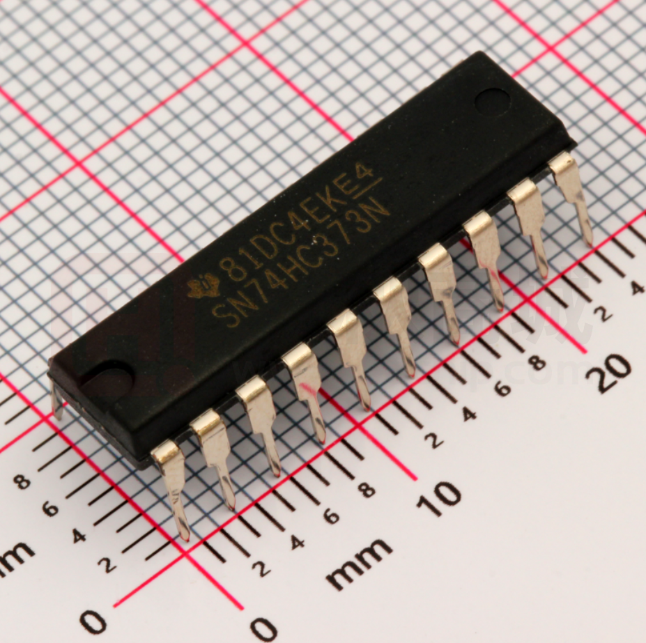
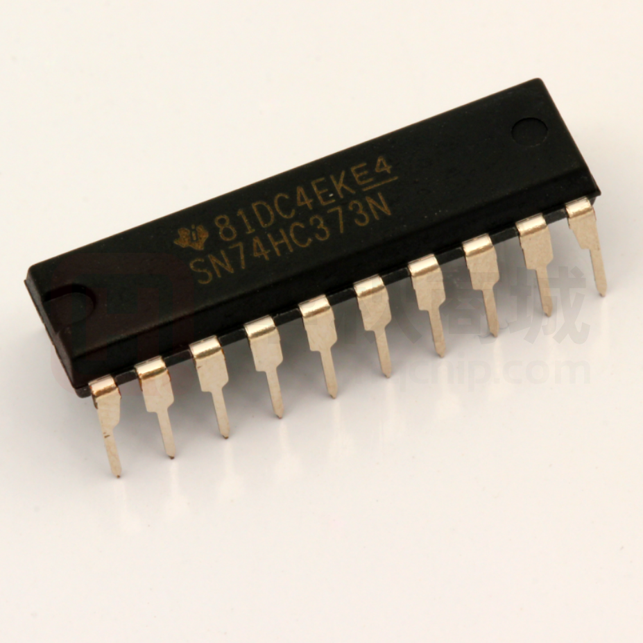
SN74HC373N
ACTIVE
PDIP
N
20
20
Pb-Free
(RoHS)
CU NIPDAU
N / A for Pkg Type
-40 to 85
SN74HC373N
SN74HC373NE4
ACTIVE
PDIP
N
20
20
Pb-Free
(RoHS)
CU NIPDAU
N / A for Pkg Type
-40 to 85
SN74HC373N
Addendum-Page 1
Samples
�PACKAGE OPTION ADDENDUM
www.ti.com
Orderable Device
24-Aug-2018
Status
(1)
Package Type Package Pins Package
Drawing
Qty
Eco Plan
Lead/Ball Finish
MSL Peak Temp
(2)
(6)
(3)
Op Temp (°C)
Device Marking
(4/5)
SN74HC373NSR
ACTIVE
SO
NS
20
2000
Green (RoHS
& no Sb/Br)
CU NIPDAU
Level-1-260C-UNLIM
-40 to 85
HC373
SN74HC373NSRE4
ACTIVE
SO
NS
20
2000
Green (RoHS
& no Sb/Br)
CU NIPDAU
Level-1-260C-UNLIM
-40 to 85
HC373
SN74HC373PW
ACTIVE
TSSOP
PW
20
70
Green (RoHS
& no Sb/Br)
CU NIPDAU
Level-1-260C-UNLIM
-40 to 85
HC373
SN74HC373PWE4
ACTIVE
TSSOP
PW
20
70
Green (RoHS
& no Sb/Br)
CU NIPDAU
Level-1-260C-UNLIM
-40 to 85
HC373
SN74HC373PWR
ACTIVE
TSSOP
PW
20
2000
Green (RoHS
& no Sb/Br)
CU NIPDAU
Level-1-260C-UNLIM
-40 to 85
HC373
SN74HC373PWRE4
ACTIVE
TSSOP
PW
20
2000
Green (RoHS
& no Sb/Br)
CU NIPDAU
Level-1-260C-UNLIM
-40 to 85
HC373
SN74HC373PWT
ACTIVE
TSSOP
PW
20
250
Green (RoHS
& no Sb/Br)
CU NIPDAU
Level-1-260C-UNLIM
-40 to 85
HC373
SNJ54HC373FK
ACTIVE
LCCC
FK
20
1
TBD
POST-PLATE
N / A for Pkg Type
-55 to 125
84072012A
SNJ54HC
373FK
SNJ54HC373J
ACTIVE
CDIP
J
20
1
TBD
A42
N / A for Pkg Type
-55 to 125
8407201RA
SNJ54HC373J
SNJ54HC373W
ACTIVE
CFP
W
20
1
TBD
A42
N / A for Pkg Type
-55 to 125
8407201SA
SNJ54HC373W
(1)
The marketing status values are defined as follows:
ACTIVE: Product device recommended for new designs.
LIFEBUY: TI has announced that the device will be discontinued, and a lifetime-buy period is in effect.
NRND: Not recommended for new designs. Device is in production to support existing customers, but TI does not recommend using this part in a new design.
PREVIEW: Device has been announced but is not in production. Samples may or may not be available.
OBSOLETE: TI has discontinued the production of the device.
(2)
RoHS: TI defines "RoHS" to mean semiconductor products that are compliant with the current EU RoHS requirements for all 10 RoHS substances, including the requirement that RoHS substance
do not exceed 0.1% by weight in homogeneous materials. Where designed to be soldered at high temperatures, "RoHS" products are suitable for use in specified lead-free processes. TI may
reference these types of products as "Pb-Free".
RoHS Exempt: TI defines "RoHS Exempt" to mean products that contain lead but are compliant with EU RoHS pursuant to a specific EU RoHS exemption.
Green: TI defines "Green" to mean the content of Chlorine (Cl) and Bromine (Br) based flame retardants meet JS709B low halogen requirements of


 工商网监
湘ICP备2023018690号
工商网监
湘ICP备2023018690号