��������� ���������
���
� ������ ����������
���� ����� ��
���
SCLS307B– JANUARY 1996 – REVISED JANUARY 2003
D
D
D
D
D
D
D
D
D
SN54HC377 . . . J OR W PACKAGE
SN74HC377 . . . DW, N, OR NS PACKAGE
(TOP VIEW)
Wide Operating Voltage Range of 2 V to 6 V
Outputs Can Drive Up To 10 LSTTL Loads
Low Power Consumption, 80-µA Max ICC
Typical tpd = 12 ns
±4-mA Output Drive at 5 V
Low Input Current of 1 µA Max
Eight Flip-Flops With Single-Rail Outputs
Clock Enable Latched to Avoid False
Clocking
Applications Include:
– Buffer/Storage Registers
– Shift Registers
– Pattern Generators
CLKEN
1Q
1D
2D
2Q
3Q
3D
4D
4Q
GND
1
20
2
19
3
18
4
17
5
16
6
15
7
14
8
13
9
12
10
11
VCC
8Q
8D
7D
7Q
6Q
6D
5D
5Q
CLK
SN54HC377 . . . FK PACKAGE
(TOP VIEW)
1D
1Q
CLKEN
VCC
8Q
description/ordering information
These devices are positive-edge-triggered octal
D-type flip-flops with an enable input. The ’HC377
devices are similar to the ’HC273 devices, but
feature a latched clock-enable (CLKEN) input
instead of a common clear.
2D
2Q
3Q
3D
4D
3 2 1 20 19
18
5
17
6
16
7
15
8
14
9 10 11 12 13
8D
7D
7Q
6Q
6D
4Q
GND
CLK
5Q
5D
Information at the data (D) inputs meeting the
setup time requirements is transferred to the
Q outputs on the positive-going edge of the clock
(CLK) pulse, if CLKEN is low. Clock triggering
occurs at a particular voltage level and is not
directly related to the transition time of the
positive-going pulse. When CLK is at either the
high or low level, the D input has no effect at the
output. These devices are designed to prevent
false clocking by transitions at CLKEN.
4
ORDERING INFORMATION
PDIP – N
–40°C
40°C to 85°C
–55°C
55 C to 125
125°C
C
ORDERABLE
PART NUMBER
PACKAGE†
TA
TOP-SIDE
MARKING
Tube
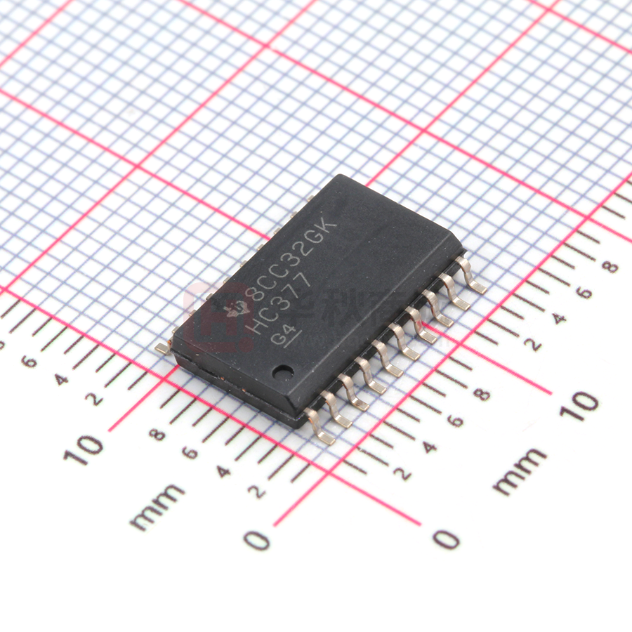
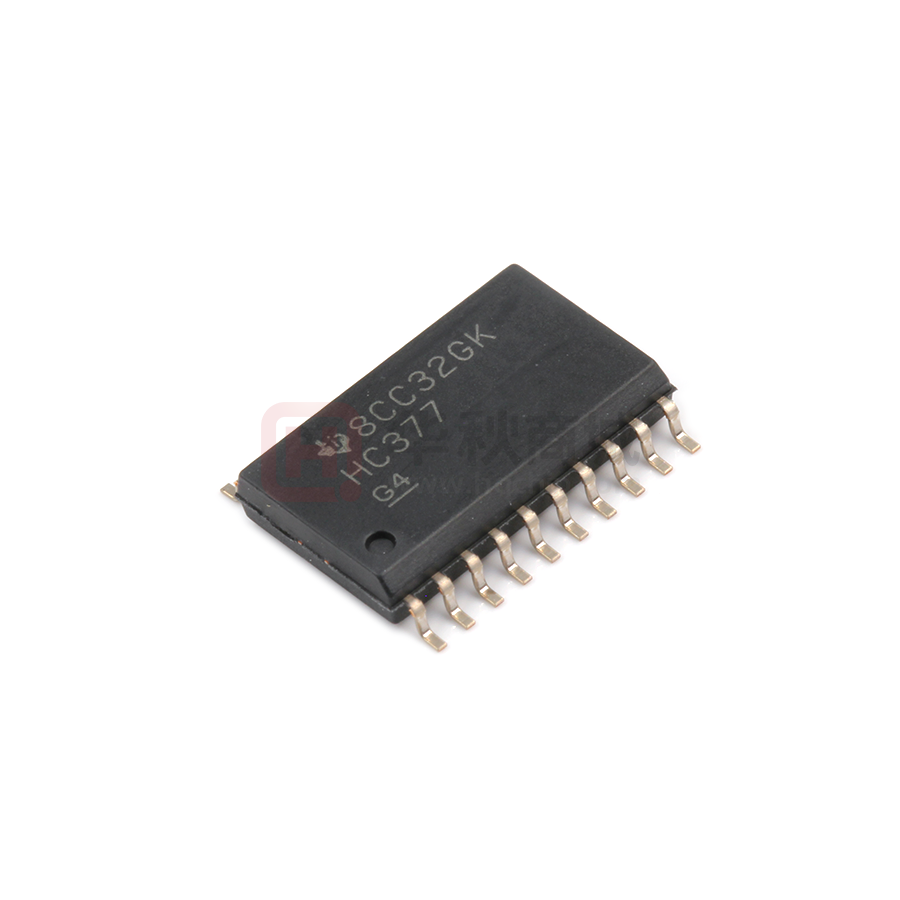
SN74HC377N
Tube
SN74HC377DW
Tape and reel
SN74HC377DWR
SOP – NS
Tape and reel
SN74HC377NSR
HC377
CDIP – J
Tube
SNJ54HC377J
SNJ54HC377J
CFP – W
Tube
SNJ54HC377W
SNJ54HC377W
SOIC – DW
SN74HC377N
HC377
LCCC – FK
Tube
SNJ54HC377FK
SNJ54HC377FK
† Package drawings, standard packing quantities, thermal data, symbolization, and PCB design guidelines are
available at www.ti.com/sc/package.
Please be aware that an important notice concerning availability, standard warranty, and use in critical applications of
Texas Instruments semiconductor products and disclaimers thereto appears at the end of this data sheet.
Copyright 2003, Texas Instruments Incorporated
���������� �
�
����� !"��� �# $%��&�" !# �� '%()�$!"��� *!"&+
���*%$"# $����� "� #'&$���$!"���# '&� ",& "&� # �� �&-!# ��#"�% &�"#
#"!�*!�* .!��!�"/+ ���*%$"��� '��$&##��0 *�&# ��" �&$&##!��)/ ��$)%*&
"&#"��0 �� !)) '!�! &"&�#+
�� '��*%$"# $� ')�!�" "� 1��������2��� !)) '!�! &"&�# !�& "&#"&*
%�)&## �",&�.�#& ��"&*+ �� !)) �",&� '��*%$"# '��*%$"���
'��$&##��0 *�&# ��" �&$&##!��)/ ��$)%*& "&#"��0 �� !)) '!�! &"&�#+
POST OFFICE BOX 655303
• DALLAS, TEXAS 75265
1
���������� ���������
���
� ������ ����������
���� ����� ��
���
SCLS307B– JANUARY 1996 – REVISED JANUARY 2003
FUNCTION TABLE
(each flip-flop)
INPUTS
CLKEN
CLK
D
OUTPUT
Q
H
X
X
Q0
L
↑
H
H
L
↑
L
L
X
L
X
Q0
logic diagram (positive logic)
CLKEN
CLK
1
11
C1
1D
3
C1
2D
4
3D
4D
13
14
7D
8D
2
16
1D
C1
18
15
1D
C1
17
12
1D
C1
6D
9
1D
C1
5D
6
1D
C1
8
5
1D
C1
7
2
1D
1D
POST OFFICE BOX 655303
• DALLAS, TEXAS 75265
19
1Q
2Q
3Q
4Q
5Q
6Q
7Q
8Q
���������� ���������
���
� ������ ����������
���� ����� ��
���
SCLS307B– JANUARY 1996 – REVISED JANUARY 2003
absolute maximum ratings over operating free-air temperature range (unless otherwise noted)†
Supply voltage range, VCC . . . . . . . . . . . . . . . . . . . . . . . . . . . . . . . . . . . . . . . . . . . . . . . . . . . . . . . . . . –0.5 V to 7 V
Input clamp current, IIK (VI < 0 or VI > VCC) (see Note 1) . . . . . . . . . . . . . . . . . . . . . . . . . . . . . . . . . . . . ±20 mA
Output clamp current, IOK (VO < 0 or VO > VCC) (see Note 1) . . . . . . . . . . . . . . . . . . . . . . . . . . . . . . . . ±20 mA
Continuous output current, IO (VO = 0 to VCC) . . . . . . . . . . . . . . . . . . . . . . . . . . . . . . . . . . . . . . . . . . . . . . ±25 mA
Continuous current through VCC or GND . . . . . . . . . . . . . . . . . . . . . . . . . . . . . . . . . . . . . . . . . . . . . . . . . . . ±50 mA
Package thermal impedance, θJA (see Note 2): DW package . . . . . . . . . . . . . . . . . . . . . . . . . . . . . . . . . 58°C/W
N package . . . . . . . . . . . . . . . . . . . . . . . . . . . . . . . . . . . 69°C/W
NS package . . . . . . . . . . . . . . . . . . . . . . . . . . . . . . . . . 60°C/W
Storage temperature range, Tstg . . . . . . . . . . . . . . . . . . . . . . . . . . . . . . . . . . . . . . . . . . . . . . . . . . . –65°C to 150°C
† Stresses beyond those listed under “absolute maximum ratings” may cause permanent damage to the device. These are stress ratings only, and
functional operation of the device at these or any other conditions beyond those indicated under “recommended operating conditions” is not
implied. Exposure to absolute-maximum-rated conditions for extended periods may affect device reliability.
NOTES: 1. The input and output voltage ratings may be exceeded if the input and output current ratings are observed.
2. The package thermal impedance is calculated in accordance with JESD 51-7.
recommended operating conditions (see Note 3)
SN54HC377
VCC
VIH
Supply voltage
High-level
High
level in
input
ut voltage
VCC = 2 V
VCC = 4.5 V
VCC = 6 V
VCC = 2 V
VIL
VI
VO
∆t/∆v
Low-level
Low
level in
input
ut voltage
MIN
NOM
MAX
2
5
6
MIN
NOM
MAX
2
5
6
1.5
1.5
3.15
3.15
4.2
4.2
VCC = 4.5 V
VCC = 6 V
Input voltage
0
Output voltage
0
Input
In
ut transition rise/fall time
SN74HC377
VCC = 2 V
VCC = 4.5 V
VCC = 6 V
0.5
1.35
1.35
1.8
1.8
0
0
V
V
0.5
VCC
VCC
UNIT
VCC
VCC
1000
1000
500
500
400
400
V
V
V
ns
TA
Operating free-air temperature
–55
125
–40
85
°C
NOTE 3: All unused inputs of the device must be held at VCC or GND to ensure proper device operation. Refer to the TI application report,
Implications of Slow or Floating CMOS Inputs, literature number SCBA004.
POST OFFICE BOX 655303
• DALLAS, TEXAS 75265
3
���������� ���������
���
� ������ ����������
���� ����� ��
���
SCLS307B– JANUARY 1996 – REVISED JANUARY 2003
electrical characteristics over recommended operating free-air temperature range (unless
otherwise noted)
PARAMETER
TEST CONDITIONS
IOH = –20
20 µA
VOH
VI = VIH or VIL
IOH = –4 mA
IOH = –5.2 mA
IOL = 20 µA
VOL
VI = VIH or VIL
IOL = 4 mA
IOL = 5.2 mA
II
ICC
VI = VCC or 0
VI = VCC or 0,
IO = 0
VCC
MIN
TA = 25°C
TYP
MAX
MIN
MAX
SN74HC377
MIN
2V
1.9
1.998
1.9
1.9
4.5 V
4.4
4.499
4.4
4.4
6V
5.9
5.999
5.9
5.9
4.5 V
3.98
4.3
3.7
3.84
6V
5.48
5.8
5.2
MAX
UNIT
V
5.34
2V
0.002
0.1
0.1
0.1
4.5 V
0.001
0.1
0.1
0.1
6V
0.001
0.1
0.1
0.1
4.5 V
0.17
0.26
0.4
0.33
6V
0.15
0.26
0.4
0.33
6V
±0.1
±100
±1000
±1000
nA
8
160
80
µA
3
10
10
10
pF
6V
Ci
SN54HC377
2 V to 6 V
V
timing requirements over recommended operating free-air temperature range (unless otherwise
noted)
VCC
fclock
tw
Clock frequency
Pulse duration, CLK high or low
D
tsu
Set p time before CLK↑
Setup
CLKEN high or low
th
4
Hold time after CLK↑
CLKEN inactive or active,, data
POST OFFICE BOX 655303
TA = 25°C
MIN
MAX
SN54HC377
MIN
MAX
SN74HC377
MIN
MAX
2V
5
3
4
4.5 V
25
16
20
6V
29
19
23
2V
100
150
125
4.5 V
20
30
25
6V
17
25
21
2V
100
150
125
4.5 V
20
30
25
6V
17
25
21
2V
100
150
125
4.5 V
20
30
25
6V
17
25
21
2V
5
5
5
4.5 V
5
5
5
6V
5
5
5
• DALLAS, TEXAS 75265
UNIT
MHz
ns
ns
ns
���������� ���������
���
� ������ ����������
���� ����� ��
���
SCLS307B– JANUARY 1996 – REVISED JANUARY 2003
switching characteristics over recommended operating free-air temperature range, CL = 50 pF
(unless otherwise noted) (see Figure 1)
PARAMETER
FROM
(INPUT)
TO
(OUTPUT)
fmax
tpd
d
tt
CLK
Any
Any
y
VCC
MIN
TA = 25°C
TYP
MAX
SN54HC377
MIN
MAX
SN74HC377
MIN
2V
5
11
3
4
4.5 V
25
54
16
20
6V
29
64
19
23
MAX
UNIT
MHz
2V
56
160
240
200
4.5 V
15
32
48
40
6V
12
27
41
34
2V
38
75
110
95
4.5 V
8
15
22
19
6V
6
13
19
16
ns
ns
operating characteristics, TA = 25°C
PARAMETER
Cpd
TEST CONDITIONS
Power dissipation capacitance per flip-flop
POST OFFICE BOX 655303
No load
• DALLAS, TEXAS 75265
TYP
30
UNIT
pF
5
���������� ���������
���
� ������ ����������
���� ����� ��
���
SCLS307B– JANUARY 1996 – REVISED JANUARY 2003
PARAMETER MEASUREMENT INFORMATION
From Output
Under Test
VCC
High-Level
Pulse
Test
Point
50%
50%
0V
tw
CL = 50 pF
(see Note A)
VCC
Low-Level
Pulse
50%
50%
0V
LOAD CIRCUIT
VOLTAGE WAVEFORMS
PULSE DURATIONS
Input
VCC
50%
50%
0V
tPLH
Reference
Input
VCC
50%
In-Phase
Output
0V
tsu
Data
Input 50%
10%
90%
tr
tPHL
VCC
50%
10% 0 V
90%
90%
tr
th
90%
50%
10%
tPHL
Out-of-Phase
Output
90%
VOLTAGE WAVEFORMS
SETUP AND HOLD AND INPUT RISE AND FALL TIMES
tPLH
50%
10%
tf
tf
VOH
50%
10%
VOL
tf
50%
10%
90%
VOH
VOL
tr
VOLTAGE WAVEFORMS
PROPAGATION DELAY AND OUTPUT TRANSITION TIMES
NOTES: A. CL includes probe and test-fixture capacitance.
B. Phase relationships between waveforms were chosen arbitrarily. All input pulses are supplied by generators having the following
characteristics: PRR ≤ 1 MHz, ZO = 50 Ω, tr = 6 ns, tf = 6 ns.
C. For clock inputs, fmax is measured when the input duty cycle is 50%.
D. The outputs are measured one at a time with one input transition per measurement.
E. tPLH and tPHL are the same as tpd.
Figure 1. Load Circuit and Voltage Waveforms
6
POST OFFICE BOX 655303
• DALLAS, TEXAS 75265
�PACKAGE OPTION ADDENDUM
www.ti.com
24-Aug-2018
PACKAGING INFORMATION
Orderable Device
Status
(1)
Package Type Package Pins Package
Drawing
Qty
Eco Plan
Lead/Ball Finish
MSL Peak Temp
(2)
(6)
(3)
Op Temp (°C)
Device Marking
(4/5)
5962-87807012A
ACTIVE
LCCC
FK
20
1
TBD
POST-PLATE
N / A for Pkg Type
-55 to 125
596287807012A
SNJ54HC
377FK
5962-8780701RA
ACTIVE
CDIP
J
20
1
TBD
A42
N / A for Pkg Type
-55 to 125
5962-8780701RA
SNJ54HC377J
SN54HC377J
ACTIVE
CDIP
J
20
1
TBD
A42
N / A for Pkg Type
-55 to 125
SN54HC377J
SN74HC377DW
ACTIVE
SOIC
DW
20
25
Green (RoHS
& no Sb/Br)
CU NIPDAU
Level-1-260C-UNLIM
-40 to 85
HC377
SN74HC377DWR
ACTIVE
SOIC
DW
20
2000
Green (RoHS
& no Sb/Br)
CU NIPDAU
Level-1-260C-UNLIM
-40 to 85
HC377
SN74HC377N
ACTIVE
PDIP
N
20
20
Pb-Free
(RoHS)
CU NIPDAU
N / A for Pkg Type
-40 to 85
SN74HC377N
SN74HC377NE4
ACTIVE
PDIP
N
20
20
Pb-Free
(RoHS)
CU NIPDAU
N / A for Pkg Type
-40 to 85
SN74HC377N
SN74HC377NSR
ACTIVE
SO
NS
20
2000
Green (RoHS
& no Sb/Br)
CU NIPDAU
Level-1-260C-UNLIM
-40 to 85
HC377
SNJ54HC377FK
ACTIVE
LCCC
FK
20
1
TBD
POST-PLATE
N / A for Pkg Type
-55 to 125
596287807012A
SNJ54HC
377FK
SNJ54HC377J
ACTIVE
CDIP
J
20
1
TBD
A42
N / A for Pkg Type
-55 to 125
5962-8780701RA
SNJ54HC377J
(1)
The marketing status values are defined as follows:
ACTIVE: Product device recommended for new designs.
LIFEBUY: TI has announced that the device will be discontinued, and a lifetime-buy period is in effect.
NRND: Not recommended for new designs. Device is in production to support existing customers, but TI does not recommend using this part in a new design.
PREVIEW: Device has been announced but is not in production. Samples may or may not be available.
OBSOLETE: TI has discontinued the production of the device.
(2)
RoHS: TI defines "RoHS" to mean semiconductor products that are compliant with the current EU RoHS requirements for all 10 RoHS substances, including the requirement that RoHS substance
do not exceed 0.1% by weight in homogeneous materials. Where designed to be soldered at high temperatures, "RoHS" products are suitable for use in specified lead-free processes. TI may
reference these types of products as "Pb-Free".
RoHS Exempt: TI defines "RoHS Exempt" to mean products that contain lead but are compliant with EU RoHS pursuant to a specific EU RoHS exemption.
Addendum-Page 1
Samples
�PACKAGE OPTION ADDENDUM
www.ti.com
24-Aug-2018
Green: TI defines "Green" to mean the content of Chlorine (Cl) and Bromine (Br) based flame retardants meet JS709B low halogen requirements of
很抱歉,暂时无法提供与“SN74HC377DWR”相匹配的价格&库存,您可以联系我们找货
免费人工找货- 国内价格 香港价格
- 1+4.146401+0.49795
- 10+2.8931310+0.34744
- 25+2.5817925+0.31005
- 100+2.24083100+0.26911
- 250+2.07923250+0.24970
- 500+1.98144500+0.23796
- 1000+1.901091000+0.22831
- 国内价格 香港价格
- 2000+1.834942000+0.22036
- 4000+1.780484000+0.21382
- 6000+1.753226000+0.21055
- 10000+1.7229910000+0.20692
- 14000+1.7053314000+0.20480
- 20000+1.6883520000+0.20276
- 50000+1.6517850000+0.19837
- 国内价格
- 1+2.97000
- 10+2.43000
- 30+2.19240
- 100+1.90080


 工商网监
湘ICP备2023018690号
工商网监
湘ICP备2023018690号