Sample &
Buy
Product
Folder
Support &
Community
Tools &
Software
Technical
Documents
SN54HC595, SN74HC595
SCLS041I – DECEMBER 1982 – REVISED SEPTEMBER 2015
SNx4HC595 8-Bit Shift Registers With 3-State Output Registers
1 Features
3 Description
•
•
•
The SNx4HC595 devices contain an 8-bit, serial-in,
parallel-out shift register that feeds an 8-bit D-type
storage register. The storage register has parallel 3state outputs. Separate clocks are provided for both
the shift and storage register. The shift register has a
direct overriding clear (SRCLR) input, serial (SER)
input, and serial outputs for cascading. When the
output-enable (OE) input is high, the outputs are in
the high-impedance state.
1
•
•
•
•
•
•
8-Bit Serial-In, Parallel-Out Shift
Wide Operating Voltage Range of 2 V to 6 V
High-Current 3-State Outputs Can Drive Up to 15
LSTTL Loads
Low Power Consumption: 80-μA (Maximum) ICC
tpd = 13 ns (Typical)
±6-mA Output Drive at 5 V
Low Input Current: 1 μA (Maximum)
Shift Register Has Direct Clear
On Products Compliant to MIL-PRF-38535,
All Parameters Are Tested Unless Otherwise
Noted. On All Other Products, Production
Processing Does Not Necessarily Include Testing
of All Parameters.
Device Information(1)
PART NUMBER
SN54HC595
SN74HC595
2 Applications
•
•
•
•
Network Switches
Power Infrastructure
LED Displays
Servers
PACKAGE
BODY SIZE (NOM)
LCCC (20)
8.89 mm x 8.89 mm
CDIP (16)
21.34 mm x 6.92 mm
PDIP (16)
19.31 mm × 6.35 mm
SOIC (16)
9.90 mm x 3.90 mm
SOIC (16)
10.30 mm x 7.50 mm
SSOP (16)
6.20 mm x 5.30 mm
TSSOP (16)
5.00 mm x 4.40 mm
(1) For all available packages, see the orderable addendum at
the end of the data sheet.
Logic Diagram (Positive Logic)
OE
RCLK
SRCLR
SRCLK
SER
13
12
10
11
14
1D
C1
R
3R
C3
3S
15
2S
2R
C2
R
3R
C3
3S
1
2S
2R
C2
R
3R
C3
3S
2
2S
2R
C2
R
3R
C3
3S
3
2S
2R
C2
R
3R
C3
3S
4
2S
2R
C2
R
3R
C3
3S
5
2S
2R
C2
R
3R
C3
3S
6
2S
2R
C2
R
3R
C3
3S
7
QA
QB
QC
9
QD
QE
QF
QG
QH
QH′
Pin numbers shown are for the D, DB, DW, J, N, NS, PW, and W packages.
1
An IMPORTANT NOTICE at the end of this data sheet addresses availability, warranty, changes, use in safety-critical applications,
intellectual property matters and other important disclaimers. PRODUCTION DATA.
�SN54HC595, SN74HC595
SCLS041I – DECEMBER 1982 – REVISED SEPTEMBER 2015
www.ti.com
Table of Contents
1
2
3
4
5
6
7
Features ..................................................................
Applications ...........................................................
Description .............................................................
Revision History.....................................................
Device Comparison Table.....................................
Pin Configuration and Functions .........................
Specifications.........................................................
7.1
7.2
7.3
7.4
7.5
7.6
7.7
7.8
7.9
8
9
1
1
1
2
3
4
5
Absolute Maximum Ratings ...................................... 5
ESD Ratings.............................................................. 5
Recommended Operating Conditions....................... 5
Thermal Information .................................................. 6
Electrical Characteristics........................................... 6
Timing Requirements ................................................ 7
Switching Characteristics .......................................... 9
Operating Characteristics.......................................... 9
Typical Characteristics ............................................ 10
Parameter Measurement Information ................ 11
Detailed Description ............................................ 12
9.1 Overview ................................................................. 12
9.2 Functional Block Diagram ....................................... 12
9.3 Feature Description................................................. 13
9.4 Device Functional Modes........................................ 13
10 Application and Implementation........................ 14
10.1 Application Information.......................................... 14
10.2 Typical Application ................................................ 14
11 Power Supply Recommendations ..................... 16
12 Layout................................................................... 16
12.1 Layout Guidelines ................................................. 16
12.2 Layout Example .................................................... 16
13 Device and Documentation Support ................. 17
13.1
13.2
13.3
13.4
13.5
13.6
Documentation Support ........................................
Related Links ........................................................
Community Resources..........................................
Trademarks ...........................................................
Electrostatic Discharge Caution ............................
Glossary ................................................................
17
17
17
17
17
17
14 Mechanical, Packaging, and Orderable
Information ........................................................... 17
4 Revision History
NOTE: Page numbers for previous revisions may differ from page numbers in the current version.
Changes from Revision H (November 2009) to Revision I
Page
•
Added Applications section, Device Information table, Pin Configuration and Functions section, ESD Ratings table,
Thermal Information table, Feature Description section, Device Functional Modes, Application and Implementation
section, Power Supply Recommendations section, Layout section, Device and Documentation Support section, and
Mechanical, Packaging, and Orderable Information section ................................................................................................. 1
•
Deleted Ordering Information table. ...................................................................................................................................... 1
•
Added Military Disclaimer to Features list. ............................................................................................................................. 1
2
Submit Documentation Feedback
Copyright © 1982–2015, Texas Instruments Incorporated
Product Folder Links: SN54HC595 SN74HC595
�SN54HC595, SN74HC595
www.ti.com
SCLS041I – DECEMBER 1982 – REVISED SEPTEMBER 2015
5 Device Comparison Table
PART NUMBER
PACKAGE
BODY SIZE (NOM)
SN54HC595FK
LCCC (20)
8.89 mm x 8.89 mm
SN54HC595J
CDIP (16)
21.34 mm x 6.92 mm
SN74HC595N
PDIP (16)
19.31 mm × 6.35 mm
SN74HC595D
SOIC (16)
9.90 mm x 3.90 mm
SN74HC595DW
SOIC (16)
10.30 mm x 7.50 mm
SN74HC595DB
SSOP (16)
6.20 mm x 5.30 mm
SN74HC595PW
TSSOP (16)
5.00 mm x 4.40 mm
Copyright © 1982–2015, Texas Instruments Incorporated
Product Folder Links: SN54HC595 SN74HC595
Submit Documentation Feedback
3
�SN54HC595, SN74HC595
SCLS041I – DECEMBER 1982 – REVISED SEPTEMBER 2015
www.ti.com
6 Pin Configuration and Functions
D, N, NS, J, DB, or PW Package
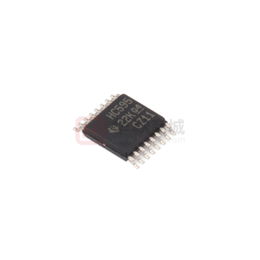
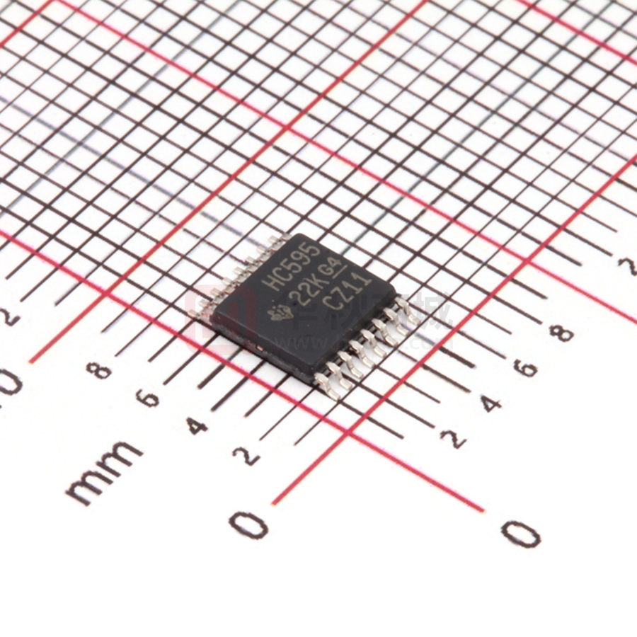
16-Pin SOIC, PDIP, SO, CDIP, SSOP, or TSSOP
Top View
FK Package
20-Pin LCCC
Top View
Pin Functions
PIN
SOIC,
PDIP, SO,
CDIP,
SSOP, or
TSSOP
LCCC
GND
8
10
—
OE
13
17
I
Output Enable
QA
15
19
O
QA Output
QB
1
2
O
QB Output
QC
2
3
O
QC Output
QD
3
4
O
QD Output
QE
4
5
O
QE Output
QF
5
7
O
QF Output
QG
6
8
O
QG Output
QH
7
9
O
QH Output
QH'
9
12
O
QH' Output
RCLK
12
14
I
RCLK Input
SER
14
18
I
SER Input
SRCLK
11
14
I
SRCLK Input
SRCLR
10
13
I
SRCLR Input
NAME
I/O
DESCRIPTION
Ground Pin
1
NC
—
VCC
—
16
11
—
No Connection
—
Power Pin
16
4
20
Submit Documentation Feedback
Copyright © 1982–2015, Texas Instruments Incorporated
Product Folder Links: SN54HC595 SN74HC595
�SN54HC595, SN74HC595
www.ti.com
SCLS041I – DECEMBER 1982 – REVISED SEPTEMBER 2015
7 Specifications
7.1 Absolute Maximum Ratings
over operating free-air temperature range (unless otherwise noted) (1)
VCC
MIN
MAX
UNIT
–0.5
7
V
VI < 0 or VI > VCC
±20
mA
VO < 0 or VO > VCC
±20
mA
VO = 0 to VCC
±35
mA
Supply voltage
(2)
IIK
Input clamp current
IOK
Output clamp current
IO
Continuous output current
(2)
Continuous current through VCC or GND
±70
mA
TJ
Junction temperature
150
°C
Tstg
Storage temperature
150
°C
(1)
(2)
–65
Stresses beyond those listed under Absolute Maximum Ratings may cause permanent damage to the device. These are stress ratings
only, and functional operation of the device at these or any other conditions beyond those indicated under Recommended Operating
Conditions is not implied. Exposure to absolute-maximum-rated conditions for extended periods may affect device reliability.
The input and output voltage ratings may be exceeded if the input and output current ratings are observed.
7.2 ESD Ratings
VALUE
Human body model (HBM), per ANSI/ESDA/JEDEC JS-001, all pins
V(ESD)
(1)
(2)
Electrostatic discharge
(1)
UNIT
2000
Charged-device model (CDM), per JEDEC specification JESD22-C101, all
pins (2)
V
1000
JEDEC document JEP155 states that 500-V HBM allows safe manufacturing with a standard ESD control process.
JEDEC document JEP157 states that 250-V CDM allows safe manufacturing with a standard ESD control process.
7.3 Recommended Operating Conditions
over operating free-air temperature range (unless otherwise noted) (1)
SN54HC595
VCC
Supply voltage
VCC = 2 V
VIH
High-level input voltage
VCC = 4.5 V
VCC = 6 V
SN74HC595
MIN
NOM
MAX
2
5
6
MIN
NOM
MAX
2
5
6
1.5
1.5
3.15
3.15
4.2
VCC = 2 V
VCC = 4.5 V
UNIT
V
V
4.2
0.5
0.5
1.35
1.35
VIL
Low-level input voltage
VI
Input voltage
0
VCC
0
VCC
V
VO
Output voltage
0
VCC
0
VCC
V
VCC = 6 V
1.8
VCC = 2 V
Δt/Δv
TA
(1)
(2)
Input transition rise or fall time (2)
Operating free-air temperature
1.8
1000
1000
VCC = 4.5 V
500
500
VCC = 6 V
400
400
–55
125
V
–40
85
ns
°C
All unused inputs of the device must be held at VCC or GND to ensure proper device operation. See the TI application report,
Implications of Slow or Floating CMOS Inputs, SCBA004.
If this device is used in the threshold region (from VILmax = 0.5 V to VIH min = 1.5 V), there is a potential to go into the wrong state from
induced grounding, causing double clocking. Operating with the inputs at tt = 1000 ns and VCC = 2 V does not damage the device;
however, functionally, the CLK inputs are not ensured while in the shift, count, or toggle operating modes.
Copyright © 1982–2015, Texas Instruments Incorporated
Product Folder Links: SN54HC595 SN74HC595
Submit Documentation Feedback
5
�SN54HC595, SN74HC595
SCLS041I – DECEMBER 1982 – REVISED SEPTEMBER 2015
www.ti.com
7.4 Thermal Information
SN74AHCT595
THERMAL METRIC
RθJA
(1)
(1)
D (SOIC)
DB
(SSOP)
DW (SOIC)
N (PDIP)
NS (SO)
PW
(TSSOP)
16 PINS
16 PINS
16 PINS
16 PINS
16 PINS
16 PINS
73
82
57
67
64
108
Junction-to-ambient thermal resistance
UNIT
°C/W
For more information about traditional and new thermal metrics, see the Semiconductor and IC Package Thermal Metrics application
report, SPRA953.
7.5 Electrical Characteristics
over recommended operating free-air temperature range (unless otherwise noted)
PARAMETER
TEST CONDITIONS
IOH = –20 μA
VOH
VI = VIH or VIL
QH′, IOH = –4 mA
QA – QH, IOH = –6 mA
QH′, IOH = −5.2 mA
QA – QH, IOH = –7.8 mA
IOL = 20 μA
VOL
VI = VIH or VIL
QH′, IOL = 4 mA
QA – QH, IOL = 6 mA
QH′, IOL = 5.2 mA
QA – QH, IOL = 7.8 mA
VCC
TA = 25°C
MIN
TYP
SN54HC595
MAX
MIN
SN74HC595
MAX
MIN
2V
1.9
1.998
1.9
1.9
4.5 V
4.4
4.499
4.4
4.4
6V
5.9
5.999
5.9
5.9
3.98
4.3
3.7
3.84
3.98
4.3
3.7
3.84
5.48
5.8
5.2
5.34
5.48
5.8
5.2
4.5 V
6V
MAX
V
5.34
2V
0.002
0.1
0.1
0.1
4.5 V
0.001
0.1
0.1
0.1
6V
0.001
0.1
0.1
0.1
0.17
0.26
0.4
0.33
0.17
0.26
0.4
0.33
0.15
0.26
0.4
0.33
0.15
0.26
0.4
0.33
4.5 V
6V
UNIT
V
II
VI = VCC or 0
6V
±0.1
±100
±1000
±1000
nA
IOZ
VO = VCC or 0, QA – QH
6V
±0.01
±0.5
±10
±5
µA
ICC
VI = VCC or 0, IO = 0
6V
8
160
80
µA
10
10
10
pF
2 V to
6V
Ci
6
Submit Documentation Feedback
3
Copyright © 1982–2015, Texas Instruments Incorporated
Product Folder Links: SN54HC595 SN74HC595
�SN54HC595, SN74HC595
www.ti.com
SCLS041I – DECEMBER 1982 – REVISED SEPTEMBER 2015
7.6 Timing Requirements
over operating free-air temperature range (unless otherwise noted)
VCC
fclock
Clock frequency
SRCLK or RCLK high or low
tw
Pulse duration
SRCLR low
SER before SRCLK↑
SRCLK↑ before RCLK↑
tsu
(1)
Set-up time
SRCLR low before RCLK↑
SRCLR high (inactive) before SRCLK↑
th
(1)
Hold time, SER after SRCLK↑
TA = 25°C
MIN
SN54HC595
MAX
MIN
MAX
SN74HC595
MIN
MAX
2V
6
4.2
5
4.5 V
31
21
25
6V
36
25
29
2V
80
120
100
4.5 V
16
24
20
6V
14
20
17
2V
80
120
100
4.5 V
16
24
20
6V
14
20
17
2V
100
150
125
4.5 V
20
30
25
6V
17
25
21
2V
75
113
94
4.5 V
15
23
19
6V
13
19
16
2V
50
75
65
4.5 V
10
15
13
6V
9
13
11
2V
50
75
60
4.5 V
10
15
12
6V
9
13
11
2V
0
0
0
4.5 V
0
0
0
6V
0
0
0
UNIT
MHz
ns
ns
ns
This set-up time allows the storage register to receive stable data from the shift register. The clocks can be tied together, in which case
the shift register is one clock pulse ahead of the storage register.
Copyright © 1982–2015, Texas Instruments Incorporated
Product Folder Links: SN54HC595 SN74HC595
Submit Documentation Feedback
7
�SN54HC595, SN74HC595
SCLS041I – DECEMBER 1982 – REVISED SEPTEMBER 2015
www.ti.com
SRCLK
SER
RCLK
SRCLR
OE
QA
QB
QC
QD
QE
QF
QG
QH
QH’
NOTE:
implies that the output is in 3-State mode.
Figure 1. Timing Diagram
8
Submit Documentation Feedback
Copyright © 1982–2015, Texas Instruments Incorporated
Product Folder Links: SN54HC595 SN74HC595
�SN54HC595, SN74HC595
www.ti.com
SCLS041I – DECEMBER 1982 – REVISED SEPTEMBER 2015
7.7 Switching Characteristics
Over recommended operating free-air temperature range.
PARAMETER
FROM
(INPUT)
TO
(OUTPUT)
tPHL
SRCLR
ten
OE
tdis
OE
2V
6
26
4.2
5
4.5 V
31
38
21
25
6V
36
42
25
29
QH′
50 pF
QA – QH
50 pF
QH′
50 pF
QA – QH
50 pF
QA – QH
50 pF
QA – QH
50 pF
tt
QH′
tpd
RCLK
ten
OE
tt
SN74HC595
50 pF
tpd
RCLK
SN54HC595
VCC
fmax
SRCLK
TA = 25°C
LOAD
CAPACITANCE
50 pF
QA – QH
150 pf
QA – QH
150 pf
QA – QH
150 pf
MIN
TYP MAX
MIN MAX
MIN
MAX
UNIT
MHz
2V
50
160
240
200
4.5 V
17
32
48
40
6V
14
27
41
34
2V
50
150
225
187
4.5 V
17
30
45
37
6V
14
26
38
32
2V
51
175
261
219
4.5 V
18
35
52
44
6V
15
30
44
37
2V
40
150
255
187
4.5 V
15
30
45
37
6V
13
26
38
32
2V
42
200
300
250
4.5 V
23
40
60
50
6V
20
34
51
43
2V
28
60
90
75
4.5 V
8
12
18
15
6V
6
10
15
13
2V
28
75
110
95
4.5 V
8
15
22
19
6V
6
13
19
16
2V
60
200
300
250
4.5 V
22
40
60
50
6V
19
34
51
43
2V
70
200
298
250
4.5 V
23
40
60
50
6V
19
34
51
43
2V
45
210
315
265
4.5 V
17
42
63
53
6V
13
36
53
45
ns
ns
ns
ns
ns
ns
ns
ns
7.8 Operating Characteristics
TA = 25°C
PARAMETER
Cpd
Power dissipation capacitance
TEST CONDITIONS
TYP
UNIT
No load
400
pF
Copyright © 1982–2015, Texas Instruments Incorporated
Product Folder Links: SN54HC595 SN74HC595
Submit Documentation Feedback
9
�SN54HC595, SN74HC595
SCLS041I – DECEMBER 1982 – REVISED SEPTEMBER 2015
www.ti.com
7.9 Typical Characteristics
40
OUTPUTS = µ+,¶�
OE = µ/2:¶�
35
30
25
20
ICC(nA) 15
10
5
0
-5
0
1
2
3
VCC(V)
4
5
6
Figure 2. SN74HC595 ICC vs. VCC
10
Submit Documentation Feedback
Copyright © 1982–2015, Texas Instruments Incorporated
Product Folder Links: SN54HC595 SN74HC595
�SN54HC595, SN74HC595
www.ti.com
SCLS041I – DECEMBER 1982 – REVISED SEPTEMBER 2015
8 Parameter Measurement Information
VCC
S1
Test
Point
From Output
Under Test
PARAMETER
RL
CL
(see Note A)
tPZH
ten
1 kΩ
tPZL
tPHZ
tdis
S2
RL
tPLZ
1 kΩ
Reference
Input
VCC
Data
Input
VCC
50%
10%
50%
VCC
0V
In-Phase
Output
50%
10%
tPHL
90%
90%
tr
tPHL
Out-ofPhase
Output
90%
Open
Closed
Closed
Open
Open
Open
VCC
th
90%
90%
VCC
50%
10% 0 V
tf
50%
10%
tf
Output
Control
(Low-Level
Enabling)
VCC
50%
50%
0V
tPZL
VOH
50%
10% V
OL
tf
Output
Waveform 1
(See Note B)
VOH
Output
Waveform 2
(See Note B)
tPLZ
90%
tr
VOL
VOLTAGE WAVEFORMS
PROPAGATION DELAY AND OUTPUT TRANSITION TIMES
≈VCC
≈VCC
50%
10%
tPZH
tPLH
50%
10%
Open
VOLTAGE WAVEFORMS
SETUP AND HOLD AND INPUT RISE AND FALL TIMES
50%
tPLH
Closed
tr
VOLTAGE WAVEFORMS
PULSE DURATIONS
50%
Closed
0V
0V
Input
Open
tsu
0V
50%
50 pF
or
150 pF
50%
50%
tw
Low-Level
Pulse
S2
50 pF
or
150 pF
LOAD CIRCUIT
50%
S1
50 pF
tpd or tt
High-Level
Pulse
CL
VOL
tPHZ
50%
90%
VOH
≈0 V
VOLTAGE WAVEFORMS
ENABLE AND DISABLE TIMES FOR 3-STATE OUTPUTS
NOTES: A. CL includes probe and test-fixture capacitance.
B. Waveform 1 is for an output with internal conditions such that the output is low, except when disabled by the output control.
Waveform 2 is for an output with internal conditions such that the output is high, except when disabled by the output control.
C. Phase relationships between waveforms were chosen arbitrarily. All input pulses are supplied by generators having the following
characteristics: PRR ≤ 1 MHz, ZO = 50 Ω, tr = 6 ns, tf = 6 ns.
D. For clock inputs, fmax is measured when the input duty cycle is 50%.
E. The outputs are measured one at a time, with one input transition per measurement.
F. t PLZ and tPHZ are the same as tdis.
G. tPZL and tPZH are the same as ten.
H. tPLH and tPHL are the same as tpd.
Figure 3. Load Circuit and Voltage Waveforms
Copyright © 1982–2015, Texas Instruments Incorporated
Product Folder Links: SN54HC595 SN74HC595
Submit Documentation Feedback
11
�SN54HC595, SN74HC595
SCLS041I – DECEMBER 1982 – REVISED SEPTEMBER 2015
www.ti.com
9 Detailed Description
9.1 Overview
The SNx4HC595 is part of the HC family of logic devices intended for CMOS applications. The SNx4HC595 is an
8-bit shift register that feeds an 8-bit D-type storage register.
Both the shift register clock (SRCLK) and storage register clock (RCLK) are positive-edge triggered. If both
clocks are connected together, the shift register always is one clock pulse ahead of the storage register.
9.2 Functional Block Diagram
OE
RCLK
SRCLR
SRCLK
SER
13
12
10
11
14
1D
C1
R
3R
C3
3S
15
2S
2R
C2
R
3R
C3
3S
1
2S
2R
C2
R
3R
C3
3S
2
2S
2R
C2
R
3R
C3
3S
3
2S
2R
C2
R
3R
C3
3S
4
2S
2R
C2
R
3R
C3
3S
5
2S
2R
C2
R
3R
C3
3S
6
2S
2R
C2
R
3R
C3
3S
7
QA
QB
QC
9
QD
QE
QF
QG
QH
QH′
Pin numbers shown are for the D, DB, DW, J, N, NS, PW, and W packages.
Figure 4. Logic Diagram (Positive Logic)
12
Submit Documentation Feedback
Copyright © 1982–2015, Texas Instruments Incorporated
Product Folder Links: SN54HC595 SN74HC595
�SN54HC595, SN74HC595
www.ti.com
SCLS041I – DECEMBER 1982 – REVISED SEPTEMBER 2015
9.3 Feature Description
The SNx4HC595 devices are 8-bit Serial-In, Parallel-Out Shift Registers. They have a wide operating current of 2
V to 6 V, and the high-current 3-state outputs can drive up to 15 LSTTL Loads. The devices have a low power
consumption of 80-μA (Maximum) ICC. Additionally, the devices have a low input current of 1 μA (Maximum) and
a ±6-mA Output Drive at 5 V.
9.4 Device Functional Modes
Table 1 lists the functional modes of the SNx4HC595 devices.
Table 1. Function Table
INPUTS
FUNCTION
SER
SRCLK
SRCLR
RCLK
OE
X
X
X
X
H
Outputs QA – QH are disabled.
X
X
X
X
L
Outputs QA – QH are enabled.
X
X
L
X
X
Shift register is cleared.
L
↑
H
X
X
First stage of the shift register goes low.
Other stages store the data of previous stage, respectively.
H
↑
H
X
X
First stage of the shift register goes high.
Other stages store the data of previous stage, respectively.
X
X
X
↑
X
Shift-register data is stored in the storage register.
Copyright © 1982–2015, Texas Instruments Incorporated
Product Folder Links: SN54HC595 SN74HC595
Submit Documentation Feedback
13
�SN54HC595, SN74HC595
SCLS041I – DECEMBER 1982 – REVISED SEPTEMBER 2015
www.ti.com
10 Application and Implementation
10.1 Application Information
The SNx4HC595 is a low-drive CMOS device that can be used for a multitude of bus interface type applications
where output ringing is a concern. The low drive and slow edge rates will minimize overshoot and undershoot on
the outputs.
10.2 Typical Application
SRCLR
SRCLK
5
RCLK
Controller
OE
SER
10
15
11
1
12
2
13
3
14
4
5
6
7
+5V
9
VCC
16
8
QA
560
QB
560
QC
QD
QE
QF
QG
QH
560
560
560
560
560
560
Q+
GND
0.1 �F
Figure 5. Typical Application Schematic
10.2.1 Design Requirements
This device uses CMOS technology and has balanced output drive. Take care to avoid bus contention because it
can drive currents that would exceed maximum limits. The high drive will also create fast edges into light loads
so routing and load conditions should be considered to prevent ringing.
10.2.2 Detailed Design Procedure
• Recommended input conditions
– Specified high and low levels. See (VIH and VIL) in the Recommended Operating Conditions table.
– Specified high and low levels. See (VIH and VIL) in the Recommended Operating Conditions table.
– Inputs are overvoltage tolerant allowing them to go as high as 5.5 V at any valid VCC
• Recommend output conditions
– Load currents should not exceed 35 mA per output and 70 mA total for the part
– Outputs should not be pulled above VCC
14
Submit Documentation Feedback
Copyright © 1982–2015, Texas Instruments Incorporated
Product Folder Links: SN54HC595 SN74HC595
�SN54HC595, SN74HC595
www.ti.com
SCLS041I – DECEMBER 1982 – REVISED SEPTEMBER 2015
Typical Application (continued)
10.2.3 Application Curves
60
50
40
30
tpd(ns)
20
10
0
0
2
4
VCC(V)
6
8
Figure 6. SN75HC595 tpd vs. VCC
Copyright © 1982–2015, Texas Instruments Incorporated
Product Folder Links: SN54HC595 SN74HC595
Submit Documentation Feedback
15
�SN54HC595, SN74HC595
SCLS041I – DECEMBER 1982 – REVISED SEPTEMBER 2015
www.ti.com
11 Power Supply Recommendations
The power supply can be any voltage between the minimum and maximum supply voltage rating located in the
Recommended Operating Conditions table.
Each VCC pin should have a good bypass capacitor to prevent power disturbance. For devices with a single
supply, 0.1 μf is recommended; if there are multiple VCC pins, then 0.01 μf or 0.022 μf is recommended for each
power pin. It is acceptable to parallel multiple bypass caps to reject different frequencies of noise. A 0.1 μf and a
1 μf are commonly used in parallel. The bypass capacitor should be installed as close to the power pin as
possible for best results.
12 Layout
12.1 Layout Guidelines
When using multiple-bit logic devices, inputs should never float.
In many cases, functions or parts of functions of digital logic devices are unused, for example, when only two
inputs of a triple-input AND gate are used or only 3 of the 4 buffer gates are used. Such input pins should not be
left unconnected because the undefined voltages at the outside connections result in undefined operational
states. Figure 7 specifies the rules that must be observed under all circumstances. All unused inputs of digital
logic devices must be connected to a high or low bias to prevent them from floating. The logic level that should
be applied to any particular unused input depends on the function of the device. Generally they will be tied to
GND or VCC, whichever makes more sense or is more convenient. It is generally acceptable to float outputs,
unless the part is a transceiver. If the transceiver has an output enable pin, it will disable the output section of the
part when asserted. This will not disable the input section of the I/Os, so they cannot float when disabled.
12.2 Layout Example
Vcc
Unused Input
Input
Output
Output
Unused Input
Input
Figure 7. Layout Diagram
16
Submit Documentation Feedback
Copyright © 1982–2015, Texas Instruments Incorporated
Product Folder Links: SN54HC595 SN74HC595
�SN54HC595, SN74HC595
www.ti.com
SCLS041I – DECEMBER 1982 – REVISED SEPTEMBER 2015
13 Device and Documentation Support
13.1 Documentation Support
13.1.1 Related Documentation
For related documentation, see the following:
Implications of Slow or Floating CMOS Inputs, SCBA004
13.2 Related Links
The table below lists quick access links. Categories include technical documents, support and community
resources, tools and software, and quick access to sample or buy.
Table 2. Related Links
PARTS
PRODUCT FOLDER
SAMPLE & BUY
TECHNICAL
DOCUMENTS
TOOLS &
SOFTWARE
SUPPORT &
COMMUNITY
SN54HC595
Click here
Click here
Click here
Click here
Click here
SN74HC595
Click here
Click here
Click here
Click here
Click here
13.3 Community Resources
The following links connect to TI community resources. Linked contents are provided "AS IS" by the respective
contributors. They do not constitute TI specifications and do not necessarily reflect TI's views; see TI's Terms of
Use.
TI E2E™ Online Community TI's Engineer-to-Engineer (E2E) Community. Created to foster collaboration
among engineers. At e2e.ti.com, you can ask questions, share knowledge, explore ideas and help
solve problems with fellow engineers.
Design Support TI's Design Support Quickly find helpful E2E forums along with design support tools and
contact information for technical support.
13.4 Trademarks
E2E is a trademark of Texas Instruments.
All other trademarks are the property of their respective owners.
13.5 Electrostatic Discharge Caution
These devices have limited built-in ESD protection. The leads should be shorted together or the device placed in conductive foam
during storage or handling to prevent electrostatic damage to the MOS gates.
13.6 Glossary
SLYZ022 — TI Glossary.
This glossary lists and explains terms, acronyms, and definitions.
14 Mechanical, Packaging, and Orderable Information
The following pages include mechanical packaging and orderable information. This information is the most
current data available for the designated devices. This data is subject to change without notice and revision of
this document. For browser based versions of this data sheet, refer to the left hand navigation.
Copyright © 1982–2015, Texas Instruments Incorporated
Product Folder Links: SN54HC595 SN74HC595
Submit Documentation Feedback
17
�PACKAGE OPTION ADDENDUM
www.ti.com
6-Feb-2020
PACKAGING INFORMATION
Orderable Device
Status
(1)
Package Type Package Pins Package
Drawing
Qty
Eco Plan
Lead/Ball Finish
MSL Peak Temp
(2)
(6)
(3)
Op Temp (°C)
Device Marking
(4/5)
5962-86816012A
ACTIVE
LCCC
FK
20
1
TBD
POST-PLATE
N / A for Pkg Type
-55 to 125
596286816012A
SNJ54HC
595FK
5962-8681601EA
ACTIVE
CDIP
J
16
1
TBD
Call TI
N / A for Pkg Type
-55 to 125
5962-8681601EA
SNJ54HC595J
5962-8681601VEA
ACTIVE
CDIP
J
16
1
TBD
Call TI
N / A for Pkg Type
-55 to 125
5962-8681601VE
A
SNV54HC595J
5962-8681601VFA
ACTIVE
CFP
W
16
1
TBD
Call TI
N / A for Pkg Type
-55 to 125
5962-8681601VF
A
SNV54HC595W
SN54HC595J
ACTIVE
CDIP
J
16
1
TBD
Call TI
N / A for Pkg Type
-55 to 125
SN54HC595J
SN74HC595D
ACTIVE
SOIC
D
16
40
Green (RoHS
& no Sb/Br)
NIPDAU
Level-1-260C-UNLIM
-40 to 85
HC595
SN74HC595DBR
ACTIVE
SSOP
DB
16
2000
Green (RoHS
& no Sb/Br)
NIPDAU
Level-1-260C-UNLIM
-40 to 85
HC595
SN74HC595DBRE4
ACTIVE
SSOP
DB
16
2000
Green (RoHS
& no Sb/Br)
NIPDAU
Level-1-260C-UNLIM
-40 to 85
HC595
SN74HC595DBRG4
ACTIVE
SSOP
DB
16
2000
Green (RoHS
& no Sb/Br)
NIPDAU
Level-1-260C-UNLIM
-40 to 85
HC595
SN74HC595DE4
ACTIVE
SOIC
D
16
40
Green (RoHS
& no Sb/Br)
NIPDAU
Level-1-260C-UNLIM
-40 to 85
HC595
SN74HC595DG4
ACTIVE
SOIC
D
16
40
Green (RoHS
& no Sb/Br)
NIPDAU
Level-1-260C-UNLIM
-40 to 85
HC595
SN74HC595DR
ACTIVE
SOIC
D
16
2500
Green (RoHS
& no Sb/Br)
NIPDAU | SN
Level-1-260C-UNLIM
-40 to 85
HC595
SN74HC595DRE4
ACTIVE
SOIC
D
16
2500
Green (RoHS
& no Sb/Br)
NIPDAU
Level-1-260C-UNLIM
-40 to 85
HC595
SN74HC595DRG3
ACTIVE
SOIC
D
16
2500
Green (RoHS
& no Sb/Br)
SN
Level-1-260C-UNLIM
-40 to 85
HC595
SN74HC595DRG4
ACTIVE
SOIC
D
16
2500
Green (RoHS
& no Sb/Br)
NIPDAU
Level-1-260C-UNLIM
-40 to 85
HC595
Addendum-Page 1
Samples
�PACKAGE OPTION ADDENDUM
www.ti.com
Orderable Device
6-Feb-2020
Status
(1)
Package Type Package Pins Package
Drawing
Qty
Eco Plan
Lead/Ball Finish
MSL Peak Temp
(2)
(6)
(3)
Op Temp (°C)
Device Marking
(4/5)
SN74HC595DT
ACTIVE
SOIC
D
16
250
Green (RoHS
& no Sb/Br)
NIPDAU
Level-1-260C-UNLIM
-40 to 85
HC595
SN74HC595DW
ACTIVE
SOIC
DW
16
40
Green (RoHS
& no Sb/Br)
NIPDAU
Level-1-260C-UNLIM
-40 to 85
HC595
SN74HC595DWR
ACTIVE
SOIC
DW
16
2000
Green (RoHS
& no Sb/Br)
NIPDAU
Level-1-260C-UNLIM
-40 to 85
HC595
SN74HC595DWRE4
ACTIVE
SOIC
DW
16
2000
Green (RoHS
& no Sb/Br)
NIPDAU
Level-1-260C-UNLIM
-40 to 85
HC595
SN74HC595DWRG4
ACTIVE
SOIC
DW
16
2000
Green (RoHS
& no Sb/Br)
NIPDAU
Level-1-260C-UNLIM
-40 to 85
HC595
SN74HC595N
ACTIVE
PDIP
N
16
25
Green (RoHS
& no Sb/Br)
NIPDAU | SN
N / A for Pkg Type
-40 to 85
SN74HC595N
SN74HC595NE4
ACTIVE
PDIP
N
16
25
Green (RoHS
& no Sb/Br)
NIPDAU
N / A for Pkg Type
-40 to 85
SN74HC595N
SN74HC595NSR
ACTIVE
SO
NS
16
2000
Green (RoHS
& no Sb/Br)
NIPDAU
Level-1-260C-UNLIM
-40 to 85
HC595
SN74HC595PW
ACTIVE
TSSOP
PW
16
90
Green (RoHS
& no Sb/Br)
NIPDAU
Level-1-260C-UNLIM
-40 to 85
HC595
SN74HC595PWR
ACTIVE
TSSOP
PW
16
2000
Green (RoHS
& no Sb/Br)
NIPDAU | SN
Level-1-260C-UNLIM
-40 to 85
HC595
SN74HC595PWRE4
ACTIVE
TSSOP
PW
16
2000
Green (RoHS
& no Sb/Br)
NIPDAU
Level-1-260C-UNLIM
-40 to 85
HC595
SN74HC595PWRG4
ACTIVE
TSSOP
PW
16
2000
Green (RoHS
& no Sb/Br)
NIPDAU
Level-1-260C-UNLIM
-40 to 85
HC595
SNJ54HC595FK
ACTIVE
LCCC
FK
20
1
TBD
POST-PLATE
N / A for Pkg Type
-55 to 125
596286816012A
SNJ54HC
595FK
SNJ54HC595J
ACTIVE
CDIP
J
16
1
TBD
Call TI
N / A for Pkg Type
-55 to 125
5962-8681601EA
SNJ54HC595J
(1)
The marketing status values are defined as follows:
ACTIVE: Product device recommended for new designs.
LIFEBUY: TI has announced that the device will be discontinued, and a lifetime-buy period is in effect.
NRND: Not recommended for new designs. Device is in production to support existing customers, but TI does not recommend using this part in a new design.
PREVIEW: Device has been announced but is not in production. Samples may or may not be available.
OBSOLETE: TI has discontinued the production of the device.
Addendum-Page 2
Samples
�PACKAGE OPTION ADDENDUM
www.ti.com
6-Feb-2020
(2)
RoHS: TI defines "RoHS" to mean semiconductor products that are compliant with the current EU RoHS requirements for all 10 RoHS substances, including the requirement that RoHS substance
do not exceed 0.1% by weight in homogeneous materials. Where designed to be soldered at high temperatures, "RoHS" products are suitable for use in specified lead-free processes. TI may
reference these types of products as "Pb-Free".
RoHS Exempt: TI defines "RoHS Exempt" to mean products that contain lead but are compliant with EU RoHS pursuant to a specific EU RoHS exemption.
Green: TI defines "Green" to mean the content of Chlorine (Cl) and Bromine (Br) based flame retardants meet JS709B low halogen requirements of


 工商网监
湘ICP备2023018690号
工商网监
湘ICP备2023018690号

