0
登录后你可以
  • 下载海量资料
  • 学习在线课程
  • 观看技术视频
  • 写文章/发帖/加入社区
会员中心
创作中心
发布
  • 发文章

  • 发资料

  • 发帖

  • 提问

  • 发视频

创作活动
SN74HCT125DR

SN74HCT125DR

  • 厂商:

    BURR-BROWN(德州仪器)

  • 封装:

    SOIC14_150MIL

  • 描述:

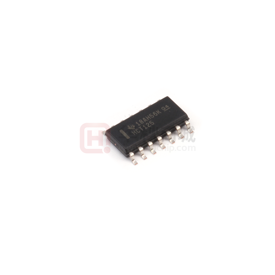
    类型:缓冲器,非反相 电源电压:4.5V~5.5V 输出类型:三态 低电平输出电流(IOL):6mA 高电平输出电流(IOH):6mA

  • 详情介绍
  • 数据手册
  • 价格&库存
SN74HCT125DR 数据手册
SN54HCT125, SN74HCT125 QUADRUPLE BUS BUFFER GATES WITH 3-STATE OUTPUTS SCLS069E – NOVEMBER 1988 – REVISED AUGUST 2003 D D D D Operating Voltage Range of 4.5 V to 5.5 V High-Current Outputs Drive Up To 15 LSTTL Loads Low Power Consumption, 80-µA Max ICC Typical tpd = 12 ns D D D D ±6-mA Output Drive at 5 V Low Input Current of 1 µA Max Inputs Are TTL-Voltage Compatible High-Current 3-State Outputs Drive Bus Lines or Buffer Memory Address Registers SN54HCT125 . . . FK PACKAGE (TOP VIEW) 1 14 2 13 3 12 4 11 5 10 6 9 7 8 VCC 4OE 4A 4Y 3OE 3A 3Y 1Y NC 2OE NC 2A 4 3 2 1 20 19 18 5 17 6 16 7 15 8 14 9 10 11 12 13 4A NC 4Y NC 3OE 2Y GND NC 3Y 3A 1OE 1A 1Y 2OE 2A 2Y GND 1A 1OE NC VCC 4OE SN54HCT125 . . . J OR W PACKAGE SN74HCT125 . . . D OR N PACKAGE (TOP VIEW) NC – No internal connection description/ordering information These bus buffer gates feature independent line drivers with 3-state outputs. Each output is disabled when the associated output-enable (OE) input is high. To ensure the high-impedance state during power up or power down, OE should be tied to VCC through a pullup resistor; the minimum value of the resistor is determined by the current-sinking capability of the driver. ORDERING INFORMATION PACKAGE† TA PDIP – N –40 C to 85 C –40°C 85°C –55°C 125°C –55 C to 125 C ORDERABLE PART NUMBER TOP-SIDE MARKING Tube of 25 SN74HCT125N Tube of 50 SN74HCT125D Reel of 2500 SN74HCT125DR Reel of 250 SN74HCT125DT CDIP – J Tube of 25 SNJ54HCT125J SNJ54HCT125J CFP – W Tube of 150 SNJ54HCT125W SNJ54HCT125W LCCC – FK Tube of 55 SNJ54HCT125FK SOIC – D SN74HCT125N HCT125 SNJ54HCT125FK † Package drawings, standard packing quantities, thermal data, symbolization, and PCB design guidelines are available at www.ti.com/sc/package. Please be aware that an important notice concerning availability, standard warranty, and use in critical applications of Texas Instruments semiconductor products and disclaimers thereto appears at the end of this data sheet. Copyright  2003, Texas Instruments Incorporated UNLESS OTHERWISE NOTED this document contains PRODUCTION DATA information current as of publication date. Products conform to specifications per the terms of Texas Instruments standard warranty. Production processing does not necessarily include testing of all parameters. POST OFFICE BOX 655303 • DALLAS, TEXAS 75265 1 SN54HCT125, SN74HCT125 QUADRUPLE BUS BUFFER GATES WITH 3-STATE OUTPUTS SCLS069E – NOVEMBER 1988 – REVISED AUGUST 2003 FUNCTION TABLE (each gate) INPUTS OE A OUTPUT Y L H H L L L H X Z logic diagram (positive logic) OE A Y absolute maximum ratings over operating free-air temperature range (unless otherwise noted)† Supply voltage range, VCC . . . . . . . . . . . . . . . . . . . . . . . . . . . . . . . . . . . . . . . . . . . . . . . . . . . . . . . . . . –0.5 V to 7 V Input clamp current, IIK (VI < 0 or VI > VCC) (see Note 1) . . . . . . . . . . . . . . . . . . . . . . . . . . . . . . . . . . . . ±20 mA Output clamp current, IOK (VO < 0 or VO > VCC) (see Note 1) . . . . . . . . . . . . . . . . . . . . . . . . . . . . . . . . ±20 mA Continuous output current, IO (VO = 0 to VCC) . . . . . . . . . . . . . . . . . . . . . . . . . . . . . . . . . . . . . . . . . . . . . . ±35 mA Continuous current through VCC or GND . . . . . . . . . . . . . . . . . . . . . . . . . . . . . . . . . . . . . . . . . . . . . . . . . . . ±70 mA Package thermal impedance, θJA (see Note 2): D package . . . . . . . . . . . . . . . . . . . . . . . . . . . . . . . . . . . 86°C/W N package . . . . . . . . . . . . . . . . . . . . . . . . . . . . . . . . . . . 80°C/W Storage temperature range, Tstg . . . . . . . . . . . . . . . . . . . . . . . . . . . . . . . . . . . . . . . . . . . . . . . . . . . –65°C to 150°C † Stresses beyond those listed under “absolute maximum ratings” may cause permanent damage to the device. These are stress ratings only, and functional operation of the device at these or any other conditions beyond those indicated under “recommended operating conditions” is not implied. Exposure to absolute-maximum-rated conditions for extended periods may affect device reliability. NOTES: 1. The input and output voltage ratings may be exceeded if the input and output current ratings are observed. 2. The package thermal impedance is calculated in accordance with JESD 51-7. recommended operating conditions (see Note 3) SN54HCT125 MIN NOM MAX MIN NOM MAX 4.5 5 5.5 4.5 5 5.5 VCC VIH Supply voltage VIL VI Low-level input voltage Input voltage 0 VO tt Output voltage 0 High-level input voltage VCC = 4.5 V to 5.5 V VCC = 4.5 V to 5.5 V SN74HCT125 2 2 0.8 Input transition (rise and fall) time VCC VCC 500 0 0 UNIT V V 0.8 V VCC VCC V 500 ns V TA Operating free-air temperature –55 125 –40 85 °C NOTE 3: All unused inputs of the device must be held at VCC or GND to ensure proper device operation. Refer to the TI application report, Implications of Slow or Floating CMOS Inputs, literature number SCBA004. PRODUCT PREVIEW information concerns products in the formative or design phase of development. Characteristic data and other specifications are design goals. Texas Instruments reserves the right to change or discontinue these products without notice. 2 POST OFFICE BOX 655303 • DALLAS, TEXAS 75265 SN54HCT125, SN74HCT125 QUADRUPLE BUS BUFFER GATES WITH 3-STATE OUTPUTS SCLS069E – NOVEMBER 1988 – REVISED AUGUST 2003 electrical characteristics over recommended operating free-air temperature range (unless otherwise noted) PARAMETER TEST CONDITIONS VCC VOH VI = VIH or VIL IOH = –20 µA IOH = –6 mA 4.5 V VOL VI = VIH or VIL IOL = 20 µA IOL = 6 mA 4.5 V II IOZ VI = VCC or 0 VO = VCC or 0, ICC VI = VCC or 0, One input at 0.5 V or 2.4 V, Other inputs at 0 or VCC ∆ICC† VI = VIH or VIL IO = 0 MIN SN54HCT125 MIN MAX SN74HCT125 MIN 4.4 4.499 4.4 4.4 3.98 4.3 3.7 3.84 MAX UNIT V 0.001 0.1 0.1 0.1 0.17 0.26 0.4 0.33 5.5 V ±0.1 ±100 ±1000 ±1000 nA 5.5 V ±0.01 ±0.5 ±10 ±5 µA 8 160 80 µA 1.4 2.4 3 2.9 mA 3 10 10* 10 pF 5.5 V 5.5 V 4.5 V to 5.5 V Ci TA = 25°C TYP MAX V * On products compliant to MIL-PRF-38535, this parameter is not production tested. † This is the increase in supply current for each input that is at one of the specified TTL voltage levels, rather than 0 V or VCC. switching characteristics over recommended operating free-air temperature range, CL = 50 pF (unless otherwise noted) (see Figure 1) PARAMETER FROM (INPUT) TO (OUTPUT) tpd A Y ten OE Y tdis OE Y tt Any VCC MIN TA = 25°C TYP MAX SN54HCT125 MIN MAX SN74HCT125 MIN MAX 4.5 V 15 26 39 33 5.5 V 12 23 35 30 4.5 V 18 28 42 35 5.5 V 15 25 38 31 4.5 V 15 26 39 33 5.5 V 13 23 35 30 4.5 V 8 15 22 19 5.5 V 7 14 21 17 UNIT ns ns ns ns switching characteristics over recommended operating free-air temperature range, CL = 150 pF (unless otherwise noted) (see Figure 1) PARAMETER FROM (INPUT) TO (OUTPUT) tpd A Y ten OE Y tt Any VCC MIN TA = 25°C TYP MAX SN54HCT125 MIN MAX SN74HCT125 MIN MAX 4.5 V 19 36 58 46 5.5 V 16 32 48 42 4.5 V 25 40 60 50 5.5 V 21 35 53 43 4.5 V 17 42 63 53 5.5 V 14 38 57 48 UNIT ns ns ns operating characteristics, TA = 25°C PARAMETER Cpd TEST CONDITIONS Power dissipation capacitance No load TYP 35 UNIT pF PRODUCT PREVIEW information concerns products in the formative or design phase of development. Characteristic data and other specifications are design goals. Texas Instruments reserves the right to change or discontinue these products without notice. POST OFFICE BOX 655303 • DALLAS, TEXAS 75265 3 SN54HCT125, SN74HCT125 QUADRUPLE BUS BUFFER GATES WITH 3-STATE OUTPUTS SCLS069E – NOVEMBER 1988 – REVISED AUGUST 2003 PARAMETER MEASUREMENT INFORMATION VCC PARAMETER tPZH ten S1 From Output Under Test CL (see Note A) 1 kΩ tPZL RL tPHZ tdis CL S1 S2 50 pF or 150 pF Open Closed Closed Open Open Closed Closed Open Open Open RL 1 kΩ 50 pF tPLZ S2 tpd or tt –– 50 pF or 150 pF LOAD CIRCUIT 3V 1.3 V Input 1.3 V 0V tPZL 3V Input 1.3 V 1.3 V 0V tPLH Output 1.3 V 10% tPHL 90% 90% tr Output Waveform 1 (See Note B) tPLZ ≈VCC 1.3 V 10% tPZH VOH 1.3 V 10% V OL tf VOLTAGE WAVEFORMS PROPAGATION DELAY TIMES Output Waveform 2 (See Note B) VOL tPHZ 1.3 V 90% VOH ≈0 V VOLTAGE WAVEFORMS ENABLE AND DISABLE TIMES FOR 3-STATE OUTPUTS NOTES: A. CL includes probe and jig capacitance. B. Waveform 1 is for an output with internal conditions such that the output is low except when disabled by the output control. Waveform 2 is for an output with internal conditions such that the output is high except when disabled by the output control. C. Phase relationships between waveforms were chosen arbitrarily. All input pulses are supplied by generators having the following characteristics: PRR ≤ 1 MHz, ZO = 50 Ω, tr = 6 ns, tf = 6 ns. D. The outputs are measured one at a time with one input transition per measurement. E. tPLZ and tPHZ are the same as tdis. F. tPZL and tPZH are the same as ten. G. tPLH and tPHL are the same as tpd. Figure 1. Load Circuit and Voltage Waveforms 4 POST OFFICE BOX 655303 • DALLAS, TEXAS 75265 PACKAGE OPTION ADDENDUM www.ti.com 24-Aug-2018 PACKAGING INFORMATION Orderable Device Status (1) Package Type Package Pins Package Drawing Qty Eco Plan Lead/Ball Finish MSL Peak Temp (2) (6) (3) Op Temp (°C) Device Marking (4/5) SN74HCT125D ACTIVE SOIC D 14 50 Green (RoHS & no Sb/Br) CU NIPDAU Level-1-260C-UNLIM -40 to 85 HCT125 SN74HCT125DE4 ACTIVE SOIC D 14 50 Green (RoHS & no Sb/Br) CU NIPDAU Level-1-260C-UNLIM -40 to 85 HCT125 SN74HCT125DG4 ACTIVE SOIC D 14 50 Green (RoHS & no Sb/Br) CU NIPDAU Level-1-260C-UNLIM -40 to 85 HCT125 SN74HCT125DR ACTIVE SOIC D 14 2500 Green (RoHS & no Sb/Br) CU NIPDAU Level-1-260C-UNLIM -40 to 85 HCT125 SN74HCT125DRE4 ACTIVE SOIC D 14 2500 Green (RoHS & no Sb/Br) CU NIPDAU Level-1-260C-UNLIM -40 to 85 HCT125 SN74HCT125DT ACTIVE SOIC D 14 250 Green (RoHS & no Sb/Br) CU NIPDAU Level-1-260C-UNLIM -40 to 85 HCT125 SN74HCT125N ACTIVE PDIP N 14 25 Green (RoHS & no Sb/Br) CU NIPDAU N / A for Pkg Type -40 to 85 SN74HCT125N SN74HCT125NE4 ACTIVE PDIP N 14 25 Green (RoHS & no Sb/Br) CU NIPDAU N / A for Pkg Type -40 to 85 SN74HCT125N (1) The marketing status values are defined as follows: ACTIVE: Product device recommended for new designs. LIFEBUY: TI has announced that the device will be discontinued, and a lifetime-buy period is in effect. NRND: Not recommended for new designs. Device is in production to support existing customers, but TI does not recommend using this part in a new design. PREVIEW: Device has been announced but is not in production. Samples may or may not be available. OBSOLETE: TI has discontinued the production of the device. (2) RoHS: TI defines "RoHS" to mean semiconductor products that are compliant with the current EU RoHS requirements for all 10 RoHS substances, including the requirement that RoHS substance do not exceed 0.1% by weight in homogeneous materials. Where designed to be soldered at high temperatures, "RoHS" products are suitable for use in specified lead-free processes. TI may reference these types of products as "Pb-Free". RoHS Exempt: TI defines "RoHS Exempt" to mean products that contain lead but are compliant with EU RoHS pursuant to a specific EU RoHS exemption. Green: TI defines "Green" to mean the content of Chlorine (Cl) and Bromine (Br) based flame retardants meet JS709B low halogen requirements of
SN74HCT125DR
物料型号: - SN54HCT125 - SN74HCT125

器件简介: 这些是四路总线缓冲器门,具有3态输出功能。每个输出在相应的输出使能(OE)输入为高电平时被禁用。为了确保上电或掉电期间的高阻态,OE应该通过上拉电阻连接到VCC;电阻的最小值由驱动器的灌电流能力决定。

引脚分配: - 1OE: 第1个输出使能 - 2OE: 第2个输出使能 - 1A, 2A, 3A, 4A: 输入端 - 1Y, 2Y, 3Y, 4Y: 输出端 - VCC: 电源电压 - GND: 地

参数特性: - 工作电压范围:4.5V 至 5.5V - 最大输入电流:1µA - 输出驱动能力:±6mA @ 5V - 典型功耗:80µA - 传播延迟:tpd = 12ns

功能详解: 每个输出都可以独立地被使能或禁用。当OE为高电平时,对应的输出将呈现高阻态,这允许在总线驱动器之间进行切换而不会相互干扰。

应用信息: 这些缓冲器门适用于驱动总线线路或缓冲存储器地址寄存器,适用于需要高电流驱动和低功耗的应用场景。

封装信息: - SN54HCT125: J 或 W 封装 - SN74HCT125: D 或 N 封装
SN74HCT125DR 价格&库存

很抱歉,暂时无法提供与“SN74HCT125DR”相匹配的价格&库存,您可以联系我们找货

免费人工找货