����������
�
���
� ����
�
�� ���
����
�
���� � ��
�
�������
SCLS562 − JANUARY 2004
D Controlled Baseline
D
D
D
D
D
D
D
D
D
D
D
D
− One Assembly/Test Site, One Fabrication
Site
Extended Temperature Performance of
−40°C to 125°C
Enhanced Diminishing Manufacturing
Sources (DMS) Support
Enhanced Product-Change Notification
Qualification Pedigree†
Operating Voltage Range of 4.5 V to 5.5 V
High-Current Outputs Drive Up To 15
LSTTL Loads
Low Power Consumption, 160-µA Max ICC
Typical tpd = 13 ns
±6-mA Output Drive at 5 V
Low Input Current of 1 µA Max
Inputs Are TTL-Voltage Compatible
3-State Outputs Drive Bus Lines or Buffer
Memory Address Registers
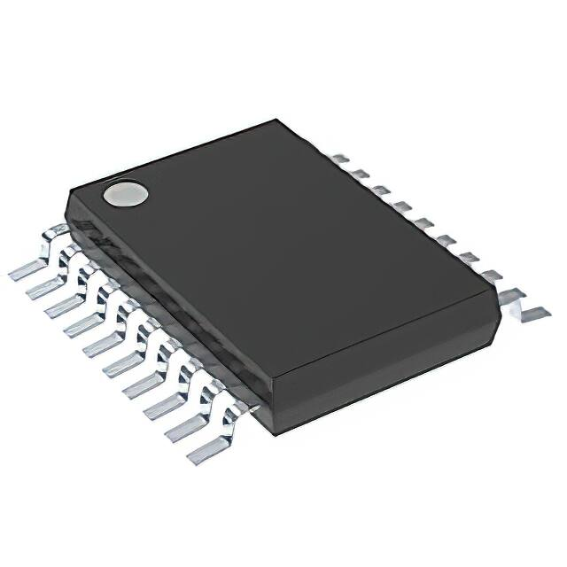
PW PACKAGE
(TOP VIEW)
1OE
1A1
2Y4
1A2
2Y3
1A3
2Y2
1A4
2Y1
GND
† Component qualification in accordance with JEDEC and industry
standards to ensure reliable operation over an extended
temperature range. This includes, but is not limited to, Highly
Accelerated Stress Test (HAST) or biased 85/85, temperature
cycle, autoclave or unbiased HAST, electromigration, bond
intermetallic life, and mold compound life. Such qualification
testing should not be viewed as justifying use of this component
beyond specified performance and environmental limits.
1
20
2
19
3
18
4
17
5
16
6
15
7
14
8
13
9
12
10
11
VCC
2OE
1Y1
2A4
1Y2
2A3
1Y3
2A2
1Y4
2A1
description/ordering information
This octal buffer and line driver is designed specifically to improve both the performance and density of 3-state
memory address drivers, clock drivers, and bus-oriented receivers and transmitters. The SN74HCT244 device
is organized as two 4-bit buffers/drivers, with separate output-enable (OE) inputs. When OE is low, the device
passes noninverted data from the A inputs to the Y outputs. When OE is high, the outputs are in the
high-impedance state.
ORDERING INFORMATION
TA
ORDERABLE
PART NUMBER
PACKAGE‡
TOP-SIDE
MARKING
−40°C to 125°C
TSSOP − PW
Tape and reel
SN74HCT244QPWREP
SHT244EP
‡ Package drawings, standard packing quantities, thermal data, symbolization, and PCB design guidelines are
available at www.ti.com/sc/package.
FUNCTION TABLE
(each buffer/driver)
INPUTS
OE
A
OUTPUT
Y
L
H
H
L
L
L
H
X
Z
Please be aware that an important notice concerning availability, standard warranty, and use in critical applications of
Texas Instruments semiconductor products and disclaimers thereto appears at the end of this data sheet.
Copyright 2004, Texas Instruments Incorporated
���������� �
�
����������� �! "#��$�� �! �� %#&'�"����� (��$)
���(#"�! "������ �� !%$"���"�����! %$� �*$ �$��! �� �$+�! ��!��#�$��!
!���(��( ,������-) ���(#"���� %��"$!!��. (�$! ��� �$"$!!���'- ��"'#($
�$!���. �� �'' %����$�$�!)
POST OFFICE BOX 655303
• DALLAS, TEXAS 75265
1
�����������
�
���
� ����
�
�� ���
����
�
���� � ��
�
�������
SCLS562 − JANUARY 2004
logic diagram (positive logic)
1OE
1A1
1A2
1A3
1A4
1
2OE
2
18
4
16
6
14
8
12
1Y1
2A1
1Y2
2A2
1Y3
2A3
1Y4
2A4
19
11
9
13
7
15
5
17
3
2Y1
2Y2
2Y3
2Y4
absolute maximum ratings over operating free-air temperature range (unless otherwise noted)†
Supply voltage range, VCC . . . . . . . . . . . . . . . . . . . . . . . . . . . . . . . . . . . . . . . . . . . . . . . . . . . . . . . . . . −0.5 V to 7 V
Input clamp current, IIK (VI < 0 or VI > VCC) (see Note 1) . . . . . . . . . . . . . . . . . . . . . . . . . . . . . . . . . . . . ±20 mA
Output clamp current, IOK (VO < 0 or VO > VCC) (see Note 1) . . . . . . . . . . . . . . . . . . . . . . . . . . . . . . . . ±20 mA
Continuous output current, IO (VO = 0 to VCC) . . . . . . . . . . . . . . . . . . . . . . . . . . . . . . . . . . . . . . . . . . . . . . ±35 mA
Continuous current through VCC or GND . . . . . . . . . . . . . . . . . . . . . . . . . . . . . . . . . . . . . . . . . . . . . . . . . . . ±70 mA
Package thermal impedance, θJA (see Note 2) . . . . . . . . . . . . . . . . . . . . . . . . . . . . . . . . . . . . . . . . . . . . . 83°C/W
Storage temperature range, Tstg . . . . . . . . . . . . . . . . . . . . . . . . . . . . . . . . . . . . . . . . . . . . . . . . . . . −65°C to 150°C
† Stresses beyond those listed under “absolute maximum ratings” may cause permanent damage to the device. These are stress ratings only, and
functional operation of the device at these or any other conditions beyond those indicated under “recommended operating conditions” is not
implied. Exposure to absolute-maximum-rated conditions for extended periods may affect device reliability.
NOTES: 1. The input and output voltage ratings may be exceeded if the input and output current ratings are observed.
2. The package thermal impedance is calculated in accordance with JESD 51-7.
recommended operating conditions (see Note 3)
MIN
NOM
MAX
4.5
5
5.5
VCC
VIH
Supply voltage
VIL
VI
Low-level input voltage
Input voltage
0
VO
∆t/∆v
Output voltage
0
High-level input voltage
VCC = 4.5 V to 5.5 V
VCC = 4.5 V to 5.5 V
Input transition rise/fall time
2
UNIT
V
V
0.8
V
VCC
VCC
V
500
ns
V
TA
Operating free-air temperature
−40
125
°C
NOTE 3: All unused inputs of the device must be held at VCC or GND to ensure proper device operation. Refer to the TI application report,
Implications of Slow or Floating CMOS Inputs, literature number SCBA004.
2
POST OFFICE BOX 655303
• DALLAS, TEXAS 75265
�����������
�
���
� ����
�
�� ���
����
�
���� � ��
�
�������
SCLS562 − JANUARY 2004
electrical characteristics over recommended operating free-air temperature range (unless
otherwise noted)
PARAMETER
TEST CONDITIONS
VCC
VOH
VI = VIH or VIL
IOH = −20 µA
IOH = −6 mA
4.5 V
VOL
VI = VIH or VIL
IOL = 20 µA
IOL = 6 mA
4.5 V
II
IOZ
VI = VCC or 0
VO = VCC or 0,
ICC
VI = VCC or 0,
∆ICC†
MIN
TA = 25°C
TYP
MAX
MIN
4.4
4.499
4.4
3.98
4.3
3.7
MAX
UNIT
V
0.001
0.1
0.1
0.17
0.26
0.4
5.5 V
±0.1
±100
±1000
nA
VI = VIH or VIL
IO = 0
5.5 V
±0.01
±0.5
±10
µA
8
160
µA
One input at 0.5 V or 2.4 V, Other inputs at 0 or VCC
5.5 V
1.4
2.4
3
mA
3
10
10
pF
5.5 V
4.5 V
to 5.5 V
Ci
V
† This is the increase in supply current for each input that is at one of the specified TTL voltage levels, rather than 0 V or VCC.
switching characteristics over recommended operating free-air temperature range, CL = 50 pF
(unless otherwise noted) (see Figure 1)
PARAMETER
FROM
(INPUT)
TO
(OUTPUT)
tpd
A
Y
ten
OE
Y
tdis
OE
Y
tt
Y
VCC
TA = 25°C
MIN
TYP
MAX
MIN
MAX
4.5 V
15
28
42
5.5 V
13
25
38
4.5 V
21
35
53
5.5 V
19
32
48
4.5 V
19
35
53
5.5 V
18
32
48
4.5 V
8
12
18
5.5 V
7
11
16
UNIT
ns
ns
ns
ns
switching characteristics over recommended operating free-air temperature range, CL = 150 pF
(unless otherwise noted) (see Figure 1)
PARAMETER
FROM
(INPUT)
TO
(OUTPUT)
tpd
A
Y
ten
OE
Y
tt
Y
VCC
TA = 25°C
MIN
TYP
MAX
MIN
MAX
4.5 V
21
45
68
5.5 V
18
40
61
4.5 V
25
52
79
5.5 V
22
47
71
4.5 V
17
42
63
5.5 V
14
38
57
UNIT
ns
ns
ns
operating characteristics, TA = 25°C
PARAMETER
Cpd
TEST CONDITIONS
Power dissipation capacitance per buffer/driver
POST OFFICE BOX 655303
No load
• DALLAS, TEXAS 75265
TYP
40
UNIT
pF
3
�����������
�
���
� ����
�
�� ���
����
�
���� � ��
�
�������
SCLS562 − JANUARY 2004
PARAMETER MEASUREMENT INFORMATION
VCC
From Output
Under Test
CL
(see Note A)
PARAMETER
S1
Test
Point
tPZH
ten
RL
S2
1 kΩ
tPZL
tPHZ
tdis
tPLZ
−−
LOAD CIRCUIT
2.7 V
2.7 V
S1
S2
50 pF
or
150 pF
Open
Closed
Closed
Open
Open
Closed
Closed
Open
Open
Open
1 kΩ
tpd or tt
Input 1.3 V
0.3 V
CL
RL
50 pF
50 pF
or
150 pF
3V
1.3 V
0.3 V 0 V
tr
tf
VOLTAGE WAVEFORM
INPUT RISE AND FALL TIMES
3V
Input
1.3 V
Output
Control
(Low-Level
Enabling)
1.3 V
0V
tPLH
In-Phase
Output
1.3 V
10%
tPHL
90%
90%
tr
tPHL
Out-ofPhase
Output
90%
VOH
1.3 V
10% V
OL
tf
tPLH
1.3 V
10%
1.3 V
10%
tf
90%
VOH
VOL
tr
VOLTAGE WAVEFORMS
PROPAGATION DELAY AND OUTPUT RISE AND FALL TIMES
3V
1.3 V
1.3 V
0V
tPZL
Output
Waveform 1
(See Note B)
tPLZ
≈VCC
1.3 V
10%
tPZH
Output
Waveform 2
(See Note B)
VOL
tPHZ
1.3 V
90%
VOH
≈0 V
VOLTAGE WAVEFORMS
ENABLE AND DISABLE TIMES FOR 3-STATE OUTPUTS
NOTES: A. CL includes probe and test-fixture capacitance.
B. Waveform 1 is for an output with internal conditions such that the output is low except when disabled by the output control.
Waveform 2 is for an output with internal conditions such that the output is high except when disabled by the output control.
C. Phase relationships between waveforms were chosen arbitrarily. All input pulses are supplied by generators having the following
characteristics: PRR ≤ 1 MHz, ZO = 50 Ω, tr = 6 ns, tf = 6 ns.
D. The outputs are measured one at a time with one input transition per measurement.
E. tPLZ and tPHZ are the same as tdis.
F. tPZL and tPZH are the same as ten.
G. tPLH and tPHL are the same as tpd.
Figure 1. Load Circuit and Voltage Waveforms
4
POST OFFICE BOX 655303
• DALLAS, TEXAS 75265
�PACKAGE OPTION ADDENDUM
www.ti.com
10-Dec-2020
PACKAGING INFORMATION
Orderable Device
Status
(1)
Package Type Package Pins Package
Drawing
Qty
Eco Plan
(2)
Lead finish/
Ball material
MSL Peak Temp
Op Temp (°C)
Device Marking
(3)
(4/5)
(6)
SN74HCT244QPWREP
ACTIVE
TSSOP
PW
20
2000
RoHS & Green
NIPDAU
Level-1-260C-UNLIM
-40 to 125
SHT244EP
V62/04698-01XE
ACTIVE
TSSOP
PW
20
2000
RoHS & Green
NIPDAU
Level-1-260C-UNLIM
-40 to 125
SHT244EP
(1)
The marketing status values are defined as follows:
ACTIVE: Product device recommended for new designs.
LIFEBUY: TI has announced that the device will be discontinued, and a lifetime-buy period is in effect.
NRND: Not recommended for new designs. Device is in production to support existing customers, but TI does not recommend using this part in a new design.
PREVIEW: Device has been announced but is not in production. Samples may or may not be available.
OBSOLETE: TI has discontinued the production of the device.
(2)
RoHS: TI defines "RoHS" to mean semiconductor products that are compliant with the current EU RoHS requirements for all 10 RoHS substances, including the requirement that RoHS substance
do not exceed 0.1% by weight in homogeneous materials. Where designed to be soldered at high temperatures, "RoHS" products are suitable for use in specified lead-free processes. TI may
reference these types of products as "Pb-Free".
RoHS Exempt: TI defines "RoHS Exempt" to mean products that contain lead but are compliant with EU RoHS pursuant to a specific EU RoHS exemption.
Green: TI defines "Green" to mean the content of Chlorine (Cl) and Bromine (Br) based flame retardants meet JS709B low halogen requirements of