SN74HCT244-Q1
SCLS509C – JUNE 2003 – REVISED JUNE 2022
SN74HCT244-Q1 Octal Buffer and Line Driver With 3-State Outputs
1 Features
2 Description
•
•
This octal buffer and line driver is designed
specifically to improve both the performance and
density of 3-state memory address drivers, clock
drivers, and bus-oriented receivers and transmitters.
The ’HCT244 device is organized as two 4-bit buffers/
drivers with separate output-enable (OE) inputs.
When OE is low, the device passes noninverted data
from the A inputs to the Y outputs. When OE is high,
the outputs are in the high-impedance state.
•
•
•
•
•
•
•
•
Qualified for automotive applications
ESD protection exceeds 1000 V per MIL-STD-883,
Method 3015; exceeds 200 V using machine
model (C = 200 pF, R = 0)
Operating voltage range of 4.5 V to 5.5 V
High-current outputs drive up to 15 LSTTL loads
Low power consumption, 80-μA max ICC
Typical tpd = 13 ns
±6-mA output drive at 5 V
Low input current of 1 μA max
Inputs are TTL-voltage compatible
3-state outputs drive bus lines or buffer memory
address registers
Device Information
(1)
PART NUMBER
PACKAGE
BODY SIZE (NOM)
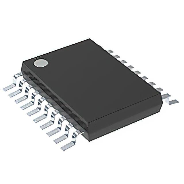
SN74HCT244QPW-Q1
TSSOP (20)
6.50 mm × 4.40 mm
(1)
For all available packages, see the orderable addendum at
the end of the data sheet.
Functional Block Diagram
An IMPORTANT NOTICE at the end of this data sheet addresses availability, warranty, changes, use in safety-critical applications,
intellectual property matters and other important disclaimers. PRODUCTION DATA.
�SN74HCT244-Q1
www.ti.com
SCLS509C – JUNE 2003 – REVISED JUNE 2022
Table of Contents
1 Features............................................................................1
2 Description.......................................................................1
3 Revision History.............................................................. 2
4 Pin Configuration and Functions...................................3
5 Specifications.................................................................. 4
5.1 Absolute Maximum Ratings........................................ 4
5.2 Recommended Operating Conditions(1) .................... 4
5.3 Thermal Information....................................................4
5.4 Electrical Characteristics.............................................5
5.5 Switching Characteristics ...........................................5
5.6 Switching Characteristics............................................5
5.7 Operating Characteristics........................................... 5
6 Parameter Measurement Information............................ 6
7 Detailed Description........................................................7
7.1 Overview..................................................................... 7
7.2 Functional Block Diagram........................................... 7
7.3 Device Functional Modes............................................7
8 Power Supply Recommendations..................................8
9 Layout...............................................................................8
9.1 Layout Guidelines....................................................... 8
10 Device and Documentation Support............................9
10.1 Receiving Notification of Documentation Updates....9
10.2 Support Resources................................................... 9
10.3 Trademarks............................................................... 9
10.4 Electrostatic Discharge Caution................................9
10.5 Glossary....................................................................9
11 Mechanical, Packaging, and Orderable
Information...................................................................... 9
3 Revision History
NOTE: Page numbers for previous revisions may differ from page numbers in the current version.
Changes from Revision B (February 2022) to Revision C (June 2022)
Page
• Junction-to-ambient thermal resistance values increased. PW was 83 is now 131.8........................................ 4
Changes from Revision A (February 2008) to Revision B (February 2022)
Page
• Updated the numbering, formatting, tables, figures, and cross-references throughout the doucment to reflect
modern data sheet standards............................................................................................................................. 1
2
Submit Document Feedback
Copyright © 2022 Texas Instruments Incorporated
Product Folder Links: SN74HCT244-Q1
�SN74HCT244-Q1
www.ti.com
SCLS509C – JUNE 2003 – REVISED JUNE 2022
4 Pin Configuration and Functions
1OE
1
20
1A1
2
19
2OE
2Y4
3
18
1Y1
1A2
2Y3
4
17
5
16
2A4
1Y2
1A3
6
15
2A3
2Y2
1A4
2Y1
GND
7
8
9
10
14
13
12
11
1Y3
2A2
1Y4
2A1
VCC
PW Package
20-Pin TSSOP
Top View
Submit Document Feedback
Copyright © 2022 Texas Instruments Incorporated
Product Folder Links: SN74HCT244-Q1
3
�SN74HCT244-Q1
www.ti.com
SCLS509C – JUNE 2003 – REVISED JUNE 2022
5 Specifications
5.1 Absolute Maximum Ratings
over operating free-air temperature range (unless otherwise noted)(1)
VCC
Supply voltage range
current(2)
MIN
MAX
–0.5
7
UNIT
V
IIK
Input clamp
VI < 0 or VI > VCC
± 20
mA
IOK
Output clamp current(2)
VO < 0 or VO > VCC
± 20
mA
IO
Continuous output current
VO = 0 to VCC
± 35
mA
± 70
mA
150
℃
150
℃
Continuous current through VCC or GND
TJ
Junction temperature
Tstg
Storage temperature range
(1)
(2)
–65
Stresses beyond those listed under “absolute maximum ratings” may cause permanent damage to the device. These are stress ratings
only, and functional operation of the device at these or any other conditions beyond those indicated under “recommended operating
conditions" is not implied. Exposure to absolute-maximum-rated conditions for extended periods may affect device reliability.
The input and output voltage ratings may be exceeded if the input and output current ratings are observed.
5.2 Recommended Operating Conditions(1)
VCC
Supply voltage
VIH
High-level input voltage
VCC = 4.5 V to 5.5 V
VIL
Low-level input voltage
VCC = 4.5 V to 5.5 V
VI
Input voltage
VO
Output voltage
Δt/Δv
Input transition rise/fall time
TA
Operating free-air temperature
(1)
MIN
NOM
MAX
4.5
5
5.5
2
UNIT
V
V
0.8
V
0
VCC
V
0
VCC
V
−40
500
ns
125
°C
All unused inputs of the device must be held at VCC or GND to ensure proper device operation. Refer to the TI application report,
Implications of Slow or Floating CMOS Inputs, literature number SCBA004.
5.3 Thermal Information
PW (TSSOP)
THERMAL METRIC
20 PINS
UNIT
RθJA
Junction-to-ambient thermal resistance
131.8
°C/W
RθJC(top)
Junction-to-case (top) thermal resistance
72.2
°C/W
RθJB
Junction-to-board thermal resistance
82.8
°C/W
ψJT
Junction-to-top characterization parameter
21.5
°C/W
ψJB
Junction-to-board characterization parameter
82.4
°C/W
RθJC(bot)
Junction-to-case (bottom) thermal resistance
N/A
°C/W
(1)
4
(1)
For more information about traditional and new thermal metrics, see the Semiconductor and IC package thermal metrics application
report.
Submit Document Feedback
Copyright © 2022 Texas Instruments Incorporated
Product Folder Links: SN74HCT244-Q1
�SN74HCT244-Q1
www.ti.com
SCLS509C – JUNE 2003 – REVISED JUNE 2022
5.4 Electrical Characteristics
over recommended operating free-air temperature range (unless otherwise noted)
PARAMETER
TEST CONDITIONS
VOH
VI = VIH or VIL
VOL
VI = VIH or VIL
II
VI = VCC or 0
IOH = −20 μA
IOH = −6 mA
IOL = 20 μA
IOL = 6 mA
TYP
4.4
4.499
4.4
3.98
4.3
3.7
MAX
UNIT
V
0.1
0.1
0.17
0.26
0.4
5.5 V
±0.1
±100
±1000
nA
±0.01
±0.5
±10
μA
8
160
μA
IOZ
VO = VCC or 0,
VI = VIH or VIL
5.5 V
VI = VCC or 0,
IO = 0
5.5 V
One input at 0.5 V or 2.4 V,
Other inputs at 0 or VCC
MAX
MIN
MIN
0.001
4.5 V
5.5 V
Ci
(1)
4.5 V
ICC
ΔICC (1)
TA = 25°C
VCC
4.5 V to 5.5 V
1.4
2.4
3
10
V
3
mA
10
pF
This is the increase in supply current for each input that is at one of the specified TTL voltage levels, rather than 0 V or VCC.
5.5 Switching Characteristics
over recommended operating free-air temperature range, CL = 50 pF (unless otherwise noted) (see Figure 6-1)
PARAMETER
FROM
(INPUT)
TO
(OUTPUT)
tpd
A
Y
ten
OE
Y
tdis
OE
Y
tt
Y
VCC
TA = 25°C
MIN
MIN
MAX
TYP
MAX
4.5 V
15
28
42
5.5 V
13
25
38
4.5 V
21
35
53
5.5 V
19
32
48
4.5 V
19
35
53
5.5 V
18
32
48
4.5 V
8
12
18
5.5 V
7
11
16
UNIT
ns
ns
ns
ns
5.6 Switching Characteristics
over recommended operating free-air temperature range, CL = 150 pF (unless otherwise noted) (see Figure 6-1)
PARAMETER
FROM
(INPUT)
TO
(OUTPUT)
tpd
A
Y
ten
OE
Y
tt
Y
VCC
TA = 25°C
MIN
MIN
MAX
TYP
MAX
4.5 V
21
45
68
5.5 V
18
40
61
4.5 V
25
52
79
5.5 V
22
47
71
4.5 V
17
42
63
5.5 V
14
38
57
UNIT
ns
ns
ns
5.7 Operating Characteristics
TA = 25℃
PARAMETER
Cpd
TEST CONDITIONS
Power dissipation capacitance per buffer/driver
No load
TYP
40
UNIT
pF
Submit Document Feedback
Copyright © 2022 Texas Instruments Incorporated
Product Folder Links: SN74HCT244-Q1
5
�SN74HCT244-Q1
www.ti.com
SCLS509C – JUNE 2003 – REVISED JUNE 2022
6 Parameter Measurement Information
A.
B.
C.
D.
E.
F.
G.
CL includes probe and test-fixture capacitance.
Waveform 1 is for an output with internal conditions such that the output is low except when disabled by the output control. Waveform 2
is for an output with internal conditions such that the output is high except when disabled by the output control.
Phase relationships between waveforms were chosen arbitrarily. All input pulses are supplied by generators having the following
characteristics: PRR ≤ 1 MHz, ZO = 50 Ω, tr = 6 ns, tf = 6 ns.
The outputs are measured one at a time with one input transition per measurement.
tPLZ and tPHZ are the same as tdis.
tPZL and tPZH are the same as ten.
tPLH and tPHL are the same as tpd.
Figure 6-1. Load Circuit and Voltage Waveforms
6
Submit Document Feedback
Copyright © 2022 Texas Instruments Incorporated
Product Folder Links: SN74HCT244-Q1
�SN74HCT244-Q1
www.ti.com
SCLS509C – JUNE 2003 – REVISED JUNE 2022
7 Detailed Description
7.1 Overview
This octal buffer and line driver is designed specifically to improve both the performance and density of 3-state
memory address drivers, clock drivers, and bus-oriented receivers and transmitters. The ’HCT244 device is
organized as two 4-bit buffers/drivers with separate output-enable (OE) inputs. When OE is low, the device
passes noninverted data from the A inputs to the Y outputs. When OE is high, the outputs are in the highimpedance state.
7.2 Functional Block Diagram
7.3 Device Functional Modes
Table 7-1. Function Table
(Each Buffer/Driver)
INPUTS
OE
A
OUTPUT
Y
L
H
H
L
L
L
H
X
Z
Submit Document Feedback
Copyright © 2022 Texas Instruments Incorporated
Product Folder Links: SN74HCT244-Q1
7
�SN74HCT244-Q1
www.ti.com
SCLS509C – JUNE 2003 – REVISED JUNE 2022
8 Power Supply Recommendations
The power supply can be any voltage between the minimum and maximum supply voltage rating located in the
Recommended Operating Conditions. Each VCC terminal should have a good bypass capacitor to prevent power
disturbance. A 0.1-μF capacitor is recommended for this device. It is acceptable to parallel multiple bypass caps
to reject different frequencies of noise. The 0.1-μF and 1-μF capacitors are commonly used in parallel. The
bypass capacitor should be installed as close to the power terminal as possible for best results.
9 Layout
9.1 Layout Guidelines
When using multiple-input and multiple-channel logic devices inputs must not ever be left floating. In many
cases, functions or parts of functions of digital logic devices are unused; for example, when only two inputs of a
triple-input AND gate are used or only 3 of the 4 buffer gates are used. Such unused input pins must not be left
unconnected because the undefined voltages at the outside connections result in undefined operational states.
All unused inputs of digital logic devices must be connected to a logic high or logic low voltage, as defined by the
input voltage specifications, to prevent them from floating. The logic level that must be applied to any particular
unused input depends on the function of the device. Generally, the inputs are tied to GND or VCC, whichever
makes more sense for the logic function or is more convenient.
8
Submit Document Feedback
Copyright © 2022 Texas Instruments Incorporated
Product Folder Links: SN74HCT244-Q1
�SN74HCT244-Q1
www.ti.com
SCLS509C – JUNE 2003 – REVISED JUNE 2022
10 Device and Documentation Support
TI offers an extensive line of development tools. Tools and software to evaluate the performance of the device,
generate code, and develop solutions are listed below.
10.1 Receiving Notification of Documentation Updates
To receive notification of documentation updates, navigate to the device product folder on ti.com. Click on
Subscribe to updates to register and receive a weekly digest of any product information that has changed. For
change details, review the revision history included in any revised document.
10.2 Support Resources
TI E2E™ support forums are an engineer's go-to source for fast, verified answers and design help — straight
from the experts. Search existing answers or ask your own question to get the quick design help you need.
Linked content is provided "AS IS" by the respective contributors. They do not constitute TI specifications and do
not necessarily reflect TI's views; see TI's Terms of Use.
10.3 Trademarks
TI E2E™ is a trademark of Texas Instruments.
All trademarks are the property of their respective owners.
10.4 Electrostatic Discharge Caution
This integrated circuit can be damaged by ESD. Texas Instruments recommends that all integrated circuits be handled
with appropriate precautions. Failure to observe proper handling and installation procedures can cause damage.
ESD damage can range from subtle performance degradation to complete device failure. Precision integrated circuits may
be more susceptible to damage because very small parametric changes could cause the device not to meet its published
specifications.
10.5 Glossary
TI Glossary
This glossary lists and explains terms, acronyms, and definitions.
11 Mechanical, Packaging, and Orderable Information
The following pages include mechanical, packaging, and orderable information. This information is the most
current data available for the designated devices. This data is subject to change without notice and revision of
this document. For browser-based versions of this data sheet, refer to the left-hand navigation.
Submit Document Feedback
Copyright © 2022 Texas Instruments Incorporated
Product Folder Links: SN74HCT244-Q1
9
�PACKAGE OPTION ADDENDUM
www.ti.com
30-Jun-2022
PACKAGING INFORMATION
Orderable Device
Status
(1)
Package Type Package Pins Package
Drawing
Qty
Eco Plan
(2)
Lead finish/
Ball material
MSL Peak Temp
Op Temp (°C)
Device Marking
(3)
Samples
(4/5)
(6)
SN74HCT244QPWRG4Q1
ACTIVE
TSSOP
PW
20
2000
RoHS & Green
NIPDAU
Level-1-260C-UNLIM
-40 to 125
HT244Q
Samples
SN74HCT244QPWRQ1
ACTIVE
TSSOP
PW
20
2000
RoHS & Green
NIPDAU
Level-3-260C-168 HR
-40 to 125
HT244Q
Samples
(1)
The marketing status values are defined as follows:
ACTIVE: Product device recommended for new designs.
LIFEBUY: TI has announced that the device will be discontinued, and a lifetime-buy period is in effect.
NRND: Not recommended for new designs. Device is in production to support existing customers, but TI does not recommend using this part in a new design.
PREVIEW: Device has been announced but is not in production. Samples may or may not be available.
OBSOLETE: TI has discontinued the production of the device.
(2)
RoHS: TI defines "RoHS" to mean semiconductor products that are compliant with the current EU RoHS requirements for all 10 RoHS substances, including the requirement that RoHS substance
do not exceed 0.1% by weight in homogeneous materials. Where designed to be soldered at high temperatures, "RoHS" products are suitable for use in specified lead-free processes. TI may
reference these types of products as "Pb-Free".
RoHS Exempt: TI defines "RoHS Exempt" to mean products that contain lead but are compliant with EU RoHS pursuant to a specific EU RoHS exemption.
Green: TI defines "Green" to mean the content of Chlorine (Cl) and Bromine (Br) based flame retardants meet JS709B low halogen requirements of