SN54HCT245, SN74HCT245
SCLS020G – MARCH 1984 – REVISED SEPTEMBER 2022
SNx4HCT245 Octal Bus Transceivers With 3-State Outputs
1 Features
3 Description
•
•
The
SNx4HCT245
octal
bus
transceivers
are
designed
for
asynchronous
two-way
communication between data buses. The controlfunction implementation minimizes external timing
requirements.
•
•
•
•
•
Operating voltage range of 4.5 V to 5.5 V
High-Current 3-state outputs drive bus lines
directly or up to 15-LSTTL loads
Low power consumption, 80-µA maximum ICC
Typical tpd = 14 ns
±6-mA output drive at 5 V
Low input current of 1 µA maximum
Inputs are TTL-voltage compatible
2 Applications
•
•
•
•
•
•
•
Factory Automation and Control
Grid Infrastructure
Electronic Point of Sale
Multi-Function Printers
Motor Drives
Storage
Telecom Infrastructure
The SNx4HCT245 devices allow data transmission
from the A bus to the B bus or from the B bus to the
A bus, depending upon the logic level at the directioncontrol (DIR) input. The output-enable ( OE) input can
be used to disable the device so that the buses are
effectively isolated.
Device Information
SN54HCT245J
J (CDIP, 20)
SN54HCT245FK
FK (LCCC, 20)
8.89 mm × 8.89 mm
SN54HCT245W
W (CFP, 20)
13.09 mm × 6.92
mm
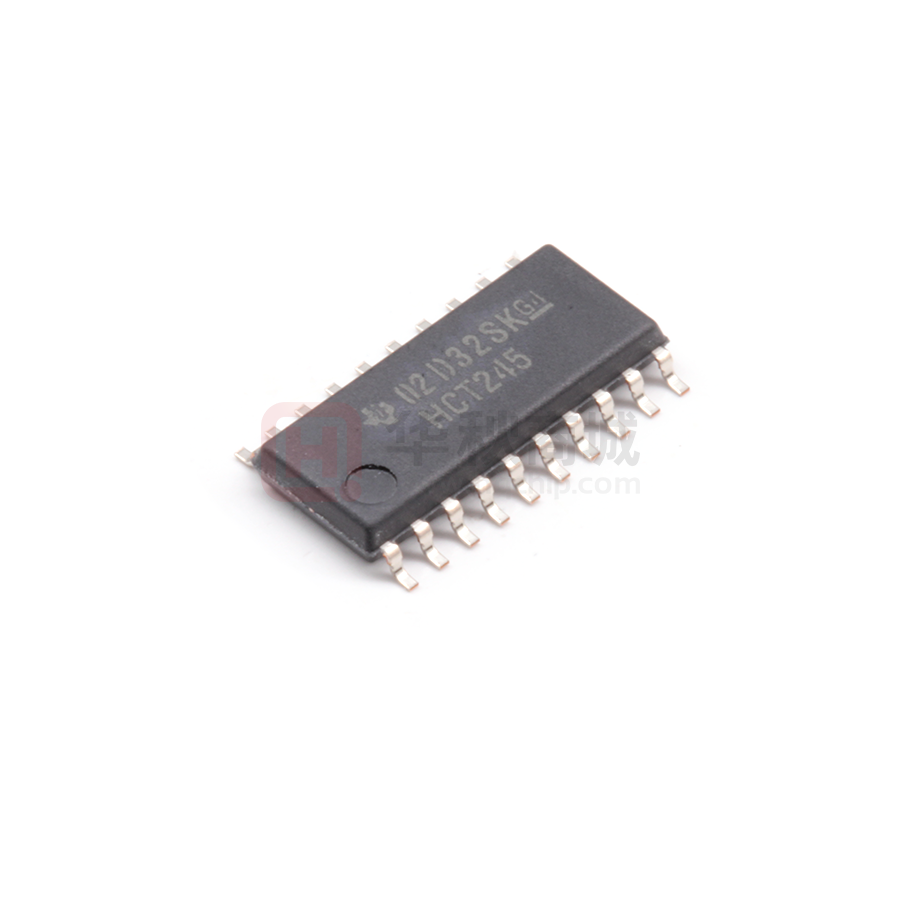
SN74HCT245DW
DW (SOIC, 20)
12.80 mm × 7.50
mm
SN74HCT245N
N (PDIP, 20)
24.33 mm × 6.35
mm
SN74HCT245NS
NS (SO, 20)
12.60 mm × 5.30
mm
SN74HCT245PW
PW (TSSOP, 20)
6.50 mm × 4.40 mm
SN74HCT245DB
DB (SSOP, 20)
7.80 mm × 7.20 mm
For all available packages, see the orderable addendum at
the end of the data sheet.
1
19
A1
BODY SIZE (NOM)
24.20 mm × 6.92
mm
(1)
DIR
PACKAGE(1)
PART NUMBER
OE
2
18
B1
To Seven Other Channels
Copyright © 2016, Texas Instruments Incorporated
Logic Diagram (Positive Logic)
An IMPORTANT NOTICE at the end of this data sheet addresses availability, warranty, changes, use in safety-critical applications,
intellectual property matters and other important disclaimers. PRODUCTION DATA.
�SN54HCT245, SN74HCT245
www.ti.com
SCLS020G – MARCH 1984 – REVISED SEPTEMBER 2022
Table of Contents
1 Features............................................................................1
2 Applications..................................................................... 1
3 Description.......................................................................1
4 Revision History.............................................................. 2
5 Pin Configuration and Functions...................................3
6 Specifications.................................................................. 4
6.1 Absolute Maximum Ratings........................................ 4
6.2 ESD Ratings............................................................... 4
6.3 Recommended Operating Conditions.........................4
6.4 Thermal Information....................................................5
6.5 Electrical Characteristics.............................................5
6.6 Switching Characteristics: CL = 50 pF........................ 6
6.7 Switching Characteristics: CL = 150 pF...................... 7
6.8 Operating Characteristics........................................... 7
6.9 Typical Characteristics................................................ 7
7 Parameter Measurement Information............................ 8
8 Detailed Description........................................................9
8.1 Overview..................................................................... 9
8.2 Functional Block Diagram........................................... 9
8.3 Feature Description.....................................................9
8.4 Device Functional Modes............................................9
9 Application and Implementation.................................. 10
9.1 Application Information............................................. 10
9.2 Typical Application.................................................... 10
10 Power Supply Recommendations..............................12
11 Layout........................................................................... 12
11.1 Layout Guidelines................................................... 12
11.2 Layout Example...................................................... 12
12 Device and Documentation Support..........................13
12.1 Documentation Support.......................................... 13
12.2 Related Links.......................................................... 13
12.3 Receiving Notification of Documentation Updates..13
12.4 Support Resources................................................. 13
12.5 Trademarks............................................................. 13
12.6 Electrostatic Discharge Caution..............................13
12.7 Glossary..................................................................13
13 Mechanical, Packaging, and Orderable
Information.................................................................... 13
4 Revision History
NOTE: Page numbers for previous revisions may differ from page numbers in the current version.
Changes from Revision F (August 2016) to Revision G (September 2022)
Page
• Updated the numbering format for tables, figures and cross-references throughout the document...................1
Changes from Revision E (August 2003) to Revision F (August 2016)
Page
• Deleted Ordering Information, see POA at the end of the datasheet................................................................. 1
• Added ESD Ratings table, Feature Description section, Device Functional Modes, Application and
Implementation section, Power Supply Recommendations section, Layout section, Device and
Documentation Support section, and Mechanical, Packaging, and Orderable Information section .................. 1
• Updated values in the Thermal Information table............................................................................................... 5
2
Submit Document Feedback
Copyright © 2022 Texas Instruments Incorporated
Product Folder Links: SN54HCT245 SN74HCT245
�SN54HCT245, SN74HCT245
www.ti.com
SCLS020G – MARCH 1984 – REVISED SEPTEMBER 2022
5 Pin Configuration and Functions
SN54HCT245 . . . J OR W PACKAGE
SN74HCT245 . . . DB, DW, N, NS, OR PW PACKAGE
(TOP VIEW)
DIR
A1
A2
A3
A4
A5
A6
A7
A8
GND
1
20
2
19
3
18
4
17
5
16
6
15
7
14
8
13
9
12
10
11
VCC
OE
B1
B2
B3
B4
B5
B6
B7
B8
4
3 2 1 20 19
18
5
17
6
16
7
15
8
14
9 10 11 12 13
B1
B2
B3
B4
B5
A8
GND
B8
B7
B6
A3
A4
A5
A6
A7
OE
A2
A1
DIR
VCC
SN54HCT245 . . . FK PACKAGE
(TOP VIEW)
Pin Functions
PIN
NO.
NAME
TYPE(1)
DESCRIPTION
1
DIR
I
2
A1
I/O
Channel 1 port A
3
A2
I/O
Channel 2 port A
4
A3
I/O
Channel 3 port A
5
A4
I/O
Channel 4 port A
6
A5
I/O
Channel 5 port A
7
A6
I/O
Channel 6 port A
8
A7
I/O
Channel 7 port A
9
A8
I/O
Channel 8 port A
10
GND
—
Ground
11
B8
O/I
Channel 8 port B
12
B7
O/I
Channel 7 port B
13
B6
O/I
Channel 6 port B
14
B5
O/I
Channel 5 port B
15
B4
O/I
Channel 4 port B
16
B3
O/I
Channel 3 port B
17
B2
O/I
Channel 2 port B
18
B1
O/I
Channel 1 port B
19
OE
I
20
VCC
—
(1)
Direction select. High = A to B, Low = B to A
Output enable, active low. High = all ports in high impedance mode, Low = all ports active
Power supply
Signal Types: I = Input, O = Output, I/O = Input or Output
Submit Document Feedback
Copyright © 2022 Texas Instruments Incorporated
Product Folder Links: SN54HCT245 SN74HCT245
3
�SN54HCT245, SN74HCT245
www.ti.com
SCLS020G – MARCH 1984 – REVISED SEPTEMBER 2022
6 Specifications
6.1 Absolute Maximum Ratings
over operating free-air temperature range (unless otherwise noted)(1)
VCC
Supply voltage
current(2)
MIN
MAX
UNIT
–0.5
7
V
IIK
Input clamp
VI < 0 or VI > VCC
±20
mA
IOK
Output clamp current(2)
VO < 0 or VO > VCC
±20
mA
IO
Continuous output current
VO = 0 to VCC
±35
mA
±70
mA
150
°C
150
°C
Continuous current through VCC or GND
TJ
Operating virtual junction temperature
Tstg
Storage temperature
(1)
(2)
–65
Stresses beyond those listed under Absolute Maximum Ratings may cause permanent damage to the device. These are stress
ratings only, which do not imply functional operation of the device at these or any other conditions beyond those indicated under
Recommended Operating Conditions. Exposure to absolute-maximum-rated conditions for extended periods may affect device
reliability.
The input and output voltage ratings may be exceeded if the input and output current ratings are observed.
6.2 ESD Ratings
VALUE
Human-body model (HBM), per ANSI/ESDA/JEDEC
V(ESD)
(1)
(2)
Electrostatic discharge
JS-001(1)
UNIT
±1500
Charged-device model (CDM), per JEDEC specification JESD22C101(2)
V
±2000
JEDEC document JEP155 states that 500-V HBM allows safe manufacturing with a standard ESD control process.
JEDEC document JEP157 states that 250-V CDM allows safe manufacturing with a standard ESD control process.
6.3 Recommended Operating Conditions
over operating free-air temperature range (unless otherwise noted)(1)
VCC
Supply voltage
VIH
High-level input voltage
VCC = 4.5 V to 5.5 V
VIL
Low-level input voltage
VCC = 4.5 V to 5.5 V
VI
Input voltage
VO
Output voltage
Δt/Δv
Input transition rise and fall time
TA
(1)
4
Operating free-air temperature
MIN
NOM
MAX
4.5
5
5.5
2
UNIT
V
V
0.8
V
0
VCC
V
0
VCC
V
500
ns
SN54HCT245
–55
125
SN74HCT245
–40
85
°C
All unused inputs of the device must be held at VCC or GND to ensure proper device operation. See the TI application report,
Implications of Slow or Floating CMOS Inputs (SCBA004).
Submit Document Feedback
Copyright © 2022 Texas Instruments Incorporated
Product Folder Links: SN54HCT245 SN74HCT245
�SN54HCT245, SN74HCT245
www.ti.com
SCLS020G – MARCH 1984 – REVISED SEPTEMBER 2022
6.4 Thermal Information
SNx4HCT245
THERMAL
J
(CDIP)
METRIC(1)
20
PINS
RθJA
Junction-to-ambient thermal resistance
RθJC(top)
Junction-to-case (top) thermal resistance
RθJB
Junction-to-board thermal resistance
ψJT
ψJB
RθJC(bot)
(1)
W
(CFP)
FK
DB
(LCCC) (SSOP)
20 PINS 20 PINS 20 PINS
—
PW
(TSSO
UNIT
P)
DW
(SOIC)
N
(PDIP)
NS
(SO)
20
PINS
20
PINS
20
PINS
20
PINS
—
—
84.6
70.4
43.4
68.9
94.9
°C/W
38.7
60.8
37.1
44.3
36.5
29.5
34.7
30.2
°C/W
49.8
100.4
36.1
40.2
38.1
24.3
36.4
45.7
°C/W
Junction-to-top characterization parameter
—
—
—
11.1
11.3
15
11.6
1.5
°C/W
Junction-to-board characterization parameter
—
—
—
39.7
37.7
24.2
36
45.1
°C/W
Junction-to-case (bottom) thermal resistance
11.5
8.5
4.3
—
—
—
—
—
°C/W
For more information about traditional and new thermal metrics, see the Semiconductor and IC Package Thermal Metrics application
report.
6.5 Electrical Characteristics
over recommended operating free-air temperature range (unless otherwise noted)
PARAMETER
TEST CONDITIONS
IOH =
–20
µA
VOH
High-Level Output Voltage
VI = VIH or VIL
VCC
MIN
TA = 25°C
4.4 4.499
SN54HCT245
4.4
SN74HCT245
TA = 25°C
4.5 V
IOH =
SN54HCT245
–6 mA
SN74HCT245
VOL
Low-Level Output Voltage
VI = VIH or VIL
TA = 25°C
IOL =
SN54HCT245
20 µA
SN74HCT245
IOL =
6 mA
TYP
TA = 25°C
4.4
3.98
Input Current
DIR or
OE
3.7
3.84
0.001
4.5 V
0.1
0.17
SN54HCT245
SN54HCT245
A or B
VO = VCC or 0
SN54HCT245
±100
±1000
5.5 V
±0.01
5.5 V
±0.5
±10
VI = VCC or 0
IO = 0 SN54HCT245
8
5.5 V
160
SN74HCT245
∆ICC (1)
Ci (2)
One input at 0.5 V TA = 25°C
or 2.4 V,
SN54HCT245
Other inputs at 0 or
SN74HCT245
VCC
Supply-Current Change
Input Capacitance
DIR or
OE
TA = 25°C
SN54HCT245
SN74HCT245
(1)
(2)
µA
±5
TA = 25°C
Supply Current
nA
±1000
SN74HCT245
ICC
V
0.33
±0.1
TA = 25°C
Off-State Output Current
0.26
0.4
SN74HCT245
IOZ
0.1
0.1
TA = 25°C
VI = VCC or 0
V
4.3
SN74HCT245
II
MAX UNIT
µA
80
1.4
2.4
3
5.5 V
mA
2.9
4.5 V
to
5.5 V
3
10
10
pF
10
This is the increase in supply current for each input that is at one of the specified TTL voltage levels, rather than 0 V or VCC.
Parameter Ci does not apply to transceiver I/O ports.
Submit Document Feedback
Copyright © 2022 Texas Instruments Incorporated
Product Folder Links: SN54HCT245 SN74HCT245
5
�SN54HCT245, SN74HCT245
www.ti.com
SCLS020G – MARCH 1984 – REVISED SEPTEMBER 2022
6.6 Switching Characteristics: CL = 50 pF
over recommended operating free-air temperature range, CL = 50 pF (unless otherwise noted) (see Figure 7-1)
PARAMETER
FROM
(INPUT)
TO
(OUTPUT)
VCC
TEST CONDITIONS
MIN
TA = 25°C
4.5 V
tpd
A or B
25
69
58
22
62
52
26
SN54HCT245
5.5 V
40
50
23
36
SN54HCT245
54
SN74HCT245
45
9
SN54HCT245
TA = 25°C
ns
12
18
15
8
11
SN54HCT245
16
SN74HCT245
14
Submit Document Feedback
ns
60
SN74HCT245
A or B
41
SN74HCT245
TA = 25°C
4.5 V
ns
46
SN54HCT245
TA = 25°C
5.5 V
6
25
SN54HCT245
SN74HCT245
A or B
20
30
TA = 25°C
4.5 V
tt
28
14
SN74HCT245
TA = 25°C
UNIT
33
SN74HCT245
A or B
5.5 V
OE
22
SN54HCT245
TA = 25°C
tdis
16
SN54HCT245
TA = 25°C
4.5 V
OE
MAX
SN74HCT245
B or A
5.5 V
ten
TYP
ns
Copyright © 2022 Texas Instruments Incorporated
Product Folder Links: SN54HCT245 SN74HCT245
�SN54HCT245, SN74HCT245
www.ti.com
SCLS020G – MARCH 1984 – REVISED SEPTEMBER 2022
6.7 Switching Characteristics: CL = 150 pF
over recommended operating free-air temperature range, CL = 150 pF (unless otherwise noted) (see Figure 7-1)
PARAMETER
FROM
(INPUT)
TO
(OUTPUT)
VCC
TEST CONDITIONS
MIN
TA = 25°C
4.5 V
tpd
A or B
30
38
18
41
SN74HCT245
34
36
SN54HCT245
80
SN74HCT245
67
17
SN54HCT245
ns
42
63
53
TA = 25°C
5.5 V
53
SN54HCT245
SN74HCT245
A or B
59
74
30
TA = 25°C
4.5 V
ns
89
TA = 25°C
5.5 V
27
SN54HCT245
SN74HCT245
A or B
UNIT
45
TA = 25°C
tt
20
SN54HCT245
TA = 25°C
4.5 V
OE
MAX
SN74HCT245
B or A
5.5 V
ten
TYP
14
38
SN54HCT245
57
SN74HCT245
48
ns
6.8 Operating Characteristics
TA = 25°C
PARAMETER
Cpd
TEST CONDITIONS
Power dissipation capacitance per transceiver
No load
TYP
40
UNIT
pF
Time (ns)
6.9 Typical Characteristics
30
29
28
27
26
25
24
23
22
21
20
19
18
17
16
4.5
Typical tpd
Maximum tpd
4.6
4.7
4.8
4.9
5
5.1
Voltage (V)
5.2
5.3
5.4
5.5
D001
Figure 6-1. Propagation Delay Over Operating Voltage Range, TA = 25°C
Submit Document Feedback
Copyright © 2022 Texas Instruments Incorporated
Product Folder Links: SN54HCT245 SN74HCT245
7
�SN54HCT245, SN74HCT245
www.ti.com
SCLS020G – MARCH 1984 – REVISED SEPTEMBER 2022
7 Parameter Measurement Information
VCC
From Output
Under Test
CL
(see Note A)
PARAMETER
S1
Test
Point
tPZH
ten
RL
1 kΩ
tPZL
tPHZ
tdis
S2
RL
tPLZ
1 kΩ
––
tpd or tt
LOAD CIRCUIT
2.7 V
Input 1.3 V
0.3 V
2.7 V
CL
S1
S2
50 pF
or
150 pF
Open
Closed
Closed
Open
Open
Closed
Closed
Open
Open
Open
50 pF
50 pF
or
150 pF
3V
1.3 V
0.3 V 0 V
tr
tf
VOLTAGE WAVEFORM
INPUT RISE AND FALL TIMES
3V
Input
1.3 V
1.3 V
0V
tPLH
In-Phase
Output
1.3 V
10%
tPHL
90%
90%
tr
Out-ofPhase
Output
tPHL
90%
VOH
1.3 V
10% V
OL
tf
tPLH
1.3 V
10%
tf
1.3 V
10%
90%
VOH
VOL
tr
VOLTAGE WAVEFORMS
PROPAGATION DELAY AND OUTPUT RISE AND FALL TIMES
A.
B.
Output
Control
(Low-Level
Enabling)
3V
1.3 V
1.3 V
0V
tPZL
tPLZ
Output
Waveform 1
(See Note B)
≈VCC
1.3 V
10%
tPZH
tPHZ
Output
Waveform 2
(See Note B)
1.3 V
90%
VOH
≈0 V
VOLTAGE WAVEFORMS
ENABLE AND DISABLE TIMES FOR 3-STATE OUTPUTS
D.
E.
CL includes probe and test-fixture capacitance.
Waveform 1 is for an output with internal conditions such that the output is low except when disabled by the output control.
Waveform 2 is for an output with internal conditions such that the output is high except when disabled by the output control.
Phase relationships between waveforms were chosen arbitrarily. All input pulses are supplied by generators having the following
characteristics: PRR ≤ 1 MHz, ZO = 50 Ω, tr = 6 ns, tf = 6 ns.
The outputs are measured one at a time with one input transition per measurement.
tPLZ and tPHZ are the same as tdis.
F.
G.
tPZL and tPZH are the same as ten.
tPLH and tPHL are the same as tpd.
C.
VOL
Figure 7-1. Load Circuit and Voltage Waveforms
8
Submit Document Feedback
Copyright © 2022 Texas Instruments Incorporated
Product Folder Links: SN54HCT245 SN74HCT245
�SN54HCT245, SN74HCT245
www.ti.com
SCLS020G – MARCH 1984 – REVISED SEPTEMBER 2022
8 Detailed Description
8.1 Overview
The SNx4HCT245 is a bidirectional buffer with direction control and active low output enable. This device is
commonly used in logic systems for isolation and increasing drive strength.
8.2 Functional Block Diagram
1
DIR
19
OE
2
A1
18
B1
To Seven Other Channels
Copyright © 2016, Texas Instruments Incorporated
Figure 8-1. Logic Diagram (Positive Logic)
8.3 Feature Description
Voltage operating range from 4.5 V to 5.5 V is forgiving of 5-V power supply rail accuracy. Outputs can operate
up to 15 LSTTL loads. This device has balanced propagation delay, typically 14 ns, and balanced output drive of
±6 mA at 5 V. It has low power consumption of only 80-µA maximum static supply current. The center VCC and
GND pin configurations minimize high-speed switching noise. Inputs are TTL-voltage compatible.
8.4 Device Functional Modes
This device is a standard '245 logic function. It has an active low output enable, a direction pin, and eight
communication channels.
Table 8-1. Function Table
INPUTS(1)
OE
(1)
DIR
OPERATION
L
L
B data to A bus
L
H
A data to B bus
H
X
Isolation
H = High Voltage Level, L = Low Voltage Level, X = Don’t Care
Submit Document Feedback
Copyright © 2022 Texas Instruments Incorporated
Product Folder Links: SN54HCT245 SN74HCT245
9
�SN54HCT245, SN74HCT245
www.ti.com
SCLS020G – MARCH 1984 – REVISED SEPTEMBER 2022
9 Application and Implementation
Note
Information in the following applications sections is not part of the TI component specification,
and TI does not warrant its accuracy or completeness. TI’s customers are responsible for
determining suitability of components for their purposes, as well as validating and testing their design
implementation to confirm system functionality.
9.1 Application Information
The SNx4HCT245 is a versatile device with many available applications. The application chosen as an example
here is connecting a master and slave device through a ribbon cable. This configuration is common due to
losses in this type of cable.
9.2 Typical Application
Logic transceivers are commonly seen in back plane and ribbon cable applications where a signal direct from
an FPGA or MCU would be too weak to reach the distant end. The transceiver acts as an amplifier to get the
signal across the line, and since it is bidirectional, data can be sent from master to slave or slave to master. The
additional buffer on the direction line is necessary to ensure the direction signal can always reach the distant
end.
Master Device
Low Drive Strength
(MCU, FPGA, CPU)
SNx4HCT245
SNx4HC245
OE
DIR
A1
B1
A1
B1
A2
B2
A2
B2
A3
B3
A3
B3
A4
B4
A4
B4
A5
B5
A5
B5
A6
B6
A6
B6
A7
B7
A7
B7
A8
B8
A8
B8
DIR
Ribbon Cable
or
Back Plane
OE
Slave Device
Copyright © 2016, Texas Instruments Incorporated
Figure 9-1. Typical application for SNx4HC245
9.2.1 Design Requirements
This device uses CMOS technology and has balanced output drive. Care must be taken to avoid bus contention
because it can drive currents that would exceed maximum limits. Outputs can be combined to produce higher
drive, but the high drive also creates faster edges into light loads, so routing and load conditions must be
considered to prevent ringing.
9.2.2 Detailed Design Procedure
1. Recommended Input Conditions
• Rise time and fall time specs: See (Δt/ΔV) in the Recommended Operating Conditions.
• Specified high and low levels: See (VIH and VIL) in the Recommended Operating Conditions.
2. Recommended Output Conditions
• Load currents should not exceed 35 mA per output and 70 mA total for the part.
• Outputs should not be pulled above VCC.
10
Submit Document Feedback
Copyright © 2022 Texas Instruments Incorporated
Product Folder Links: SN54HCT245 SN74HCT245
�SN54HCT245, SN74HCT245
www.ti.com
SCLS020G – MARCH 1984 – REVISED SEPTEMBER 2022
9.2.3 Application Curve
It is common to see significant losses in ribbon cables and back planes. The plot shown in Figure 9-2 is a
simplified simulation of a ribbon cable from a 5-V, 10-MHz low drive strength source. It shows the difference
between an input signal from a weak driver like an MCU or FPGA compared to a strong driver like the
SN74HCT245 when measured at the distant end of the cable. By adding a high-current drive transceiver before
the cable, the signal strength can be significantly improved, and subsequently the cable can be longer.
5.5
Unbuffered
SN74HCT245
5
4.5
Voltage (V)
4
3.5
3
2.5
2
1.5
1
0.5
0
0
50
100
150
200 250 300
Time (ns)
350
400
450
500
D001
Unbuffered line is directly connected to low current source, SN74HCT245 line is buffered through the transceiver. Both signals are
measured at the distant end of the ribbon cable.
Figure 9-2. Simulated Outputs From Ribbon Cable With a 5-V, 10-MHz Source
Submit Document Feedback
Copyright © 2022 Texas Instruments Incorporated
Product Folder Links: SN54HCT245 SN74HCT245
11
�SN54HCT245, SN74HCT245
www.ti.com
SCLS020G – MARCH 1984 – REVISED SEPTEMBER 2022
10 Power Supply Recommendations
The power supply can be any voltage between the MIN and MAX supply voltage rating located in the
Recommended Operating Conditions. Each VCC pin must have a good bypass capacitor to prevent power
disturbance. For devices with a single supply, 0.1 µF is recommended; if there are multiple VCC pins, then 0.01
µF or 0.022 µF is recommended for each power pin. It is acceptable to parallel multiple bypass capacitors to
reject different frequencies of noise. A 0.1 µF and a 1 µF are commonly used in parallel. The bypass capacitor
should be installed as close to the power pin as possible for best results.
11 Layout
11.1 Layout Guidelines
When using multiple-bit logic devices, inputs should never float.
In many cases, functions or parts of functions of digital logic devices are unused, for example, when only six
channels of an eight channel transceiver are used. Such input pins should not be left unconnected because the
undefined voltages at the outside connections result in undefined operational states. All unused inputs of digital
logic devices must be connected to a high or low bias to prevent them from floating. The logic level that should
be applied to any particular unused input depends on the function of the device. Generally they are tied to GND
or VCC, whichever makes more sense or is more convenient.
The output enable pin disables the output section of the part when asserted. This does not disable the input
section of the IOs, so they cannot float when disabled.
Figure 11-1 shows the proper method to terminate unused channels using a large resistance (in this example,
10-kΩ resistors). This avoids overloading the outputs , and maintains a valid voltage on the inputs. Note that it is
also valid to tie both sides of an unused transceiver directly to ground or VCC; however, the two sides must never
be tied to different states directly.
11.2 Layout Example
DIR
Master Device
SNx4HCT245
OE
A1
B1
A2
B2
A3
B3
A4
B4
A5
B5
A6
B6
A7
B7
A8
B8
Slave Device
10 k
10 k
10 k
10 k
Figure 11-1. Proper Termination of OE Pin And Unused Channels 7 and 8
12
Submit Document Feedback
Copyright © 2022 Texas Instruments Incorporated
Product Folder Links: SN54HCT245 SN74HCT245
�SN54HCT245, SN74HCT245
www.ti.com
SCLS020G – MARCH 1984 – REVISED SEPTEMBER 2022
12 Device and Documentation Support
12.1 Documentation Support
12.1.1 Related Documentation
For related documentation see the following:
Implications of Slow or Floating CMOS Inputs (SCBA004)
12.2 Related Links
The table below lists quick access links. Categories include technical documents, support and community
resources, tools and software, and quick access to sample or buy.
Table 12-1. Related Links
PARTS
PRODUCT FOLDER
SAMPLE & BUY
TECHNICAL
DOCUMENTS
TOOLS &
SOFTWARE
SUPPORT &
COMMUNITY
SN54HCT245
Click here
Click here
Click here
Click here
Click here
SN74HCT245
Click here
Click here
Click here
Click here
Click here
12.3 Receiving Notification of Documentation Updates
To receive notification of documentation updates, navigate to the device product folder on ti.com. Click on
Subscribe to updates to register and receive a weekly digest of any product information that has changed. For
change details, review the revision history included in any revised document.
12.4 Support Resources
TI E2E™ support forums are an engineer's go-to source for fast, verified answers and design help — straight
from the experts. Search existing answers or ask your own question to get the quick design help you need.
Linked content is provided "AS IS" by the respective contributors. They do not constitute TI specifications and do
not necessarily reflect TI's views; see TI's Terms of Use.
12.5 Trademarks
TI E2E™ is a trademark of Texas Instruments.
All trademarks are the property of their respective owners.
12.6 Electrostatic Discharge Caution
This integrated circuit can be damaged by ESD. Texas Instruments recommends that all integrated circuits be handled
with appropriate precautions. Failure to observe proper handling and installation procedures can cause damage.
ESD damage can range from subtle performance degradation to complete device failure. Precision integrated circuits may
be more susceptible to damage because very small parametric changes could cause the device not to meet its published
specifications.
12.7 Glossary
TI Glossary
This glossary lists and explains terms, acronyms, and definitions.
13 Mechanical, Packaging, and Orderable Information
The following pages include mechanical, packaging, and orderable information. This information is the most
current data available for the designated devices. This data is subject to change without notice and revision of
this document. For browser-based versions of this data sheet, refer to the left-hand navigation.
Submit Document Feedback
Copyright © 2022 Texas Instruments Incorporated
Product Folder Links: SN54HCT245 SN74HCT245
13
�PACKAGE OPTION ADDENDUM
www.ti.com
14-Oct-2022
PACKAGING INFORMATION
Orderable Device
Status
(1)
Package Type Package Pins Package
Drawing
Qty
Eco Plan
(2)
Lead finish/
Ball material
MSL Peak Temp
Op Temp (°C)
Device Marking
(3)
Samples
(4/5)
(6)
5962-8550601VRA
ACTIVE
CDIP
J
20
20
Non-RoHS
& Green
SNPB
N / A for Pkg Type
-55 to 125
5962-8550601VR
A
SNV54HCT245J
5962-8550601VSA
ACTIVE
CFP
W
20
25
Non-RoHS
& Green
SNPB
N / A for Pkg Type
-55 to 125
5962-8550601VS
A
SNV54HCT245W
85506012A
ACTIVE
LCCC
FK
20
1
Non-RoHS
& Green
SNPB
N / A for Pkg Type
-55 to 125
85506012A
SNJ54HCT
245FK
8550601RA
ACTIVE
CDIP
J
20
1
Non-RoHS
& Green
SNPB
N / A for Pkg Type
-55 to 125
8550601RA
SNJ54HCT245J
Samples
JM38510/65553BRA
ACTIVE
CDIP
J
20
1
Non-RoHS
& Green
SNPB
N / A for Pkg Type
-55 to 125
JM38510/
65553BRA
Samples
JM38510/65553BSA
ACTIVE
CFP
W
20
1
Non-RoHS
& Green
SNPB
N / A for Pkg Type
-55 to 125
JM38510/
65553BSA
Samples
M38510/65553BRA
ACTIVE
CDIP
J
20
1
Non-RoHS
& Green
SNPB
N / A for Pkg Type
-55 to 125
JM38510/
65553BRA
Samples
M38510/65553BSA
ACTIVE
CFP
W
20
1
Non-RoHS
& Green
SNPB
N / A for Pkg Type
-55 to 125
JM38510/
65553BSA
Samples
SN54HCT245J
ACTIVE
CDIP
J
20
1
Non-RoHS
& Green
SNPB
N / A for Pkg Type
-55 to 125
SN54HCT245J
Samples
SN74HCT245DBR
ACTIVE
SSOP
DB
20
2000
RoHS & Green
NIPDAU
Level-1-260C-UNLIM
-40 to 85
HT245
Samples
SN74HCT245DBRG4
ACTIVE
SSOP
DB
20
2000
RoHS & Green
NIPDAU
Level-1-260C-UNLIM
-40 to 85
HT245
Samples
SN74HCT245DW
ACTIVE
SOIC
DW
20
25
RoHS & Green
NIPDAU
Level-1-260C-UNLIM
-40 to 85
HCT245
Samples
SN74HCT245DWE4
ACTIVE
SOIC
DW
20
25
RoHS & Green
NIPDAU
Level-1-260C-UNLIM
-40 to 85
HCT245
Samples
SN74HCT245DWR
ACTIVE
SOIC
DW
20
2000
RoHS & Green
NIPDAU
Level-1-260C-UNLIM
-40 to 85
HCT245
Samples
SN74HCT245DWRE4
ACTIVE
SOIC
DW
20
2000
RoHS & Green
NIPDAU
Level-1-260C-UNLIM
-40 to 85
HCT245
Samples
SN74HCT245DWRG4
ACTIVE
SOIC
DW
20
2000
RoHS & Green
NIPDAU
Level-1-260C-UNLIM
-40 to 85
HCT245
Samples
SN74HCT245N
ACTIVE
PDIP
N
20
20
RoHS & Green
NIPDAU
N / A for Pkg Type
-40 to 85
SN74HCT245N
Samples
Addendum-Page 1
Samples
Samples
Samples
�PACKAGE OPTION ADDENDUM
www.ti.com
Orderable Device
14-Oct-2022
Status
(1)
Package Type Package Pins Package
Drawing
Qty
Eco Plan
(2)
Lead finish/
Ball material
MSL Peak Temp
Op Temp (°C)
Device Marking
(3)
Samples
(4/5)
(6)
SN74HCT245NE4
ACTIVE
PDIP
N
20
20
RoHS & Green
NIPDAU
N / A for Pkg Type
-40 to 85
SN74HCT245N
Samples
SN74HCT245NSR
ACTIVE
SO
NS
20
2000
RoHS & Green
NIPDAU
Level-1-260C-UNLIM
-40 to 85
HCT245
Samples
SN74HCT245PW
ACTIVE
TSSOP
PW
20
70
RoHS & Green
NIPDAU
Level-1-260C-UNLIM
-40 to 85
HT245
Samples
SN74HCT245PWR
ACTIVE
TSSOP
PW
20
2000
RoHS & Green
NIPDAU | SN
Level-1-260C-UNLIM
-40 to 85
HT245
Samples
SN74HCT245PWRE4
ACTIVE
TSSOP
PW
20
2000
RoHS & Green
NIPDAU
Level-1-260C-UNLIM
-40 to 85
HT245
Samples
SN74HCT245PWRG4
ACTIVE
TSSOP
PW
20
2000
RoHS & Green
NIPDAU
Level-1-260C-UNLIM
-40 to 85
HT245
Samples
SN74HCT245PWT
ACTIVE
TSSOP
PW
20
250
RoHS & Green
NIPDAU
Level-1-260C-UNLIM
-40 to 85
HT245
Samples
SNJ54HCT245FK
ACTIVE
LCCC
FK
20
1
Non-RoHS
& Green
SNPB
N / A for Pkg Type
-55 to 125
85506012A
SNJ54HCT
245FK
SNJ54HCT245J
ACTIVE
CDIP
J
20
1
Non-RoHS
& Green
SNPB
N / A for Pkg Type
-55 to 125
8550601RA
SNJ54HCT245J
Samples
SNJ54HCT245W
ACTIVE
CFP
W
20
1
Non-RoHS
& Green
SNPB
N / A for Pkg Type
-55 to 125
SNJ54HCT245W
Samples
(1)
The marketing status values are defined as follows:
ACTIVE: Product device recommended for new designs.
LIFEBUY: TI has announced that the device will be discontinued, and a lifetime-buy period is in effect.
NRND: Not recommended for new designs. Device is in production to support existing customers, but TI does not recommend using this part in a new design.
PREVIEW: Device has been announced but is not in production. Samples may or may not be available.
OBSOLETE: TI has discontinued the production of the device.
(2)
RoHS: TI defines "RoHS" to mean semiconductor products that are compliant with the current EU RoHS requirements for all 10 RoHS substances, including the requirement that RoHS substance
do not exceed 0.1% by weight in homogeneous materials. Where designed to be soldered at high temperatures, "RoHS" products are suitable for use in specified lead-free processes. TI may
reference these types of products as "Pb-Free".
RoHS Exempt: TI defines "RoHS Exempt" to mean products that contain lead but are compliant with EU RoHS pursuant to a specific EU RoHS exemption.
Green: TI defines "Green" to mean the content of Chlorine (Cl) and Bromine (Br) based flame retardants meet JS709B low halogen requirements of