SN74HSTL16918
9-BIT TO 18-BIT HSTL-TO-LVTTL MEMORY ADDRESS LATCH
SCES096C – APRIL 1997 – REVISED JANUARY 1999
D
D
D
D
D
DGG PACKAGE
(TOP VIEW)
Member of the Texas Instruments
Widebus Family
Inputs Meet JEDEC HSTL Std JESD 8-6 and
Outputs Meet Level III Specifications
ESD Protection Exceeds 2000 V Per
MIL-STD-883, Method 3015; Exceeds 200 V
Using Machine Model (C = 200 pF, R = 0)
Latch-Up Performance Exceeds 250 mA Per
JESD 17
Packaged in Plastic Thin Shrink
Small-Outline Package
2Q1
1Q1
GND
D1
D2
VCC
D3
D4
GND
1LE
GND
VREF
GND
2LE
GND
D5
D6
D7
VCC
D8
D9
GND
2Q9
1Q9
description
This 9-bit to 18-bit D-type latch is designed for
3.15-V to 3.45-V VCC operation. The D inputs
accept HSTL levels and the Q outputs provide
LVTTL levels.
The SN74HSTL16918 is particularly suitable for
driving an address bus to two banks of memory.
Each bank of nine outputs is controlled with its
own latch-enable (LE) input.
Each of the nine D inputs is tied to the inputs of two
D-type latches that provide true data (Q) at the
outputs. While LE is low, the Q outputs of the
corresponding nine latches follow the D inputs.
When LE is taken high, the Q outputs are latched
at the levels set up at the D inputs.
1
48
2
47
3
46
4
45
5
44
6
43
7
42
8
41
9
40
10
39
11
38
12
37
13
36
14
35
15
34
16
33
17
32
18
31
19
30
20
29
21
28
22
27
23
26
24
25
VCC
VCC
1Q2
2Q2
GND
1Q3
2Q3
VCC
1Q4
2Q4
GND
1Q5
2Q5
GND
1Q6
2Q6
VCC
1Q7
2Q7
GND
1Q8
2Q8
VCC
VCC
The SN74HSTL16918 is characterized for
operation from 0°C to 70°C.
FUNCTION TABLE
INPUTS
LE
D
OUTPUT
Q
L
H
H
L
L
H
X
L
Q0†
† Output level before the
indicated steady-state input
conditions were established
Please be aware that an important notice concerning availability, standard warranty, and use in critical applications of
Texas Instruments semiconductor products and disclaimers thereto appears at the end of this data sheet.
Widebus is a trademark of Texas Instruments Incorporated.
Copyright 1999, Texas Instruments Incorporated
PRODUCTION DATA information is current as of publication date.
Products conform to specifications per the terms of Texas Instruments
standard warranty. Production processing does not necessarily include
testing of all parameters.
POST OFFICE BOX 655303
• DALLAS, TEXAS 75265
1
�SN74HSTL16918
9-BIT TO 18-BIT HSTL-TO-LVTTL MEMORY ADDRESS LATCH
SCES096C – APRIL 1997 – REVISED JANUARY 1999
logic diagram (positive logic)
10
1LE
4
D1
1D
2
1Q1
C1
14
1D
2LE
1
2Q1
C1
To Eight Other Channels
absolute maximum ratings over operating free-air temperature range (unless otherwise noted)†
Supply voltage range, VCC . . . . . . . . . . . . . . . . . . . . . . . . . . . . . . . . . . . . . . . . . . . . . . . . . . . . . . . . . –0.5 V to 4.6 V
Input voltage range, VI (see Note 1) . . . . . . . . . . . . . . . . . . . . . . . . . . . . . . . . . . . . . . . . . . . –0.5 V to VCC + 0.5 V
Output voltage range, VO (see Note 1) . . . . . . . . . . . . . . . . . . . . . . . . . . . . . . . . . . . . . . . . –0.5 V to VCC + 0.5 V
Input clamp current, IIK (VI < 0) . . . . . . . . . . . . . . . . . . . . . . . . . . . . . . . . . . . . . . . . . . . . . . . . . . . . . . . . . . . –50 mA
Output clamp current, IOK (VO < 0 or VO > VCC) (see Note 2) . . . . . . . . . . . . . . . . . . . . . . . . . . . . . . . . ±50 mA
Continuous output current, IO (VO = 0 to VCC) . . . . . . . . . . . . . . . . . . . . . . . . . . . . . . . . . . . . . . . . . . . . . . ±50 mA
Continuous current through each VCC or GND . . . . . . . . . . . . . . . . . . . . . . . . . . . . . . . . . . . . . . . . . . . . . ±100 mA
Package thermal impedance, θJA (see Note 3) . . . . . . . . . . . . . . . . . . . . . . . . . . . . . . . . . . . . . . . . . . . . . . 89°C/W
Storage temperature range, Tstg . . . . . . . . . . . . . . . . . . . . . . . . . . . . . . . . . . . . . . . . . . . . . . . . . . . –65°C to 150°C
† Stresses beyond those listed under “absolute maximum ratings” may cause permanent damage to the device. These are stress ratings only, and
functional operation of the device at these or any other conditions beyond those indicated under “recommended operating conditions” is not
implied. Exposure to absolute-maximum-rated conditions for extended periods may affect device reliability.
NOTES: 1. The input and output negative-voltage ratings may be exceeded if the input and output clamp-current ratings are observed.
2. This current flows only when the output is in the high state and VO > VCC.
3. The package thermal impedance is calculated in accordance with JESD 51.
recommended operating conditions (see Note 4)
MIN
VCC
VREF
Supply voltage
3.15
Reference voltage
0.68
VI
VIH
Input voltage
AC high-level input voltage
All inputs
VIL
VIH
AC low-level input voltage
All inputs
DC high-level input voltage
All inputs
VIL
IOH
DC low-level input voltage
All inputs
IOL
TA
Low-level output current
0
NOM
0.75
MAX
UNIT
3.45
V
0.9
V
1.5
V
VREF+200 mV
V
VREF–200 mV
VREF+100 mV
Operating free-air temperature
V
VREF–100 mV
–24
High-level output current
0
V
V
mA
24
mA
70
°C
NOTE 4: All unused inputs of the device must be held at VCC or GND to ensure proper device operation. Refer to the TI application report,
Implications of Slow or Floating CMOS Inputs, literature number SCBA004.
2
POST OFFICE BOX 655303
• DALLAS, TEXAS 75265
�SN74HSTL16918
9-BIT TO 18-BIT HSTL-TO-LVTTL MEMORY ADDRESS LATCH
SCES096C – APRIL 1997 – REVISED JANUARY 1999
electrical characteristics over recommended operating free-air temperature range (unless
otherwise noted)
PARAMETER
TEST CONDITIONS
VIK
VOH
VCC = 3.15 V,
VCC = 3.15 V,
II = –18 mA
IOH = –24 mA
VOL
VCC = 3.15 V,
IOL = 24 mA
VI = 0 or 1.5 V
Control inputs
II
Data inputs
VCC = 3.45 V
Ci
Control inputs
Data inputs
TYP†
UNIT
–1.2
V
V
0.5
V
±5
±5
µA
90
VCC = 3.45 V,
VCC = 0 or 3.3 V,
VI = 0 or 1.5 V
VI = 0 or 3.3 V
50
VCC = 0 or 3.3 V,
VCC = 0,
VI = 0 or 3.3 V
VO = 0
2.5
Co
Outputs
† All typical values are at VCC = 3.3 V, TA = 25°C.
MAX
2.4
VI = 0 or 1.5 V
VREF = 0.68 V or 0.9 V
VREF
ICC
MIN
100
2
mA
pF
4
pF
timing requirements over recommended ranges of supply voltage and operating free-air
temperature (unless otherwise noted) (see Figure 1)
VCC = 3.3 V
± 0.15 V
MIN
tw
tsu
Pulse duration, LE low
th
tldr‡
Hold time
D after LE↑
Data race condition time
D after LE↓
Setup time, D before LE↑
UNIT
MAX
3
ns
2
ns
1
ns
0
ns
‡ This is the maximum time after LE switches low that the data input can return to the latched state from the opposite state without producing a
glitch on the output.
switching characteristics over recommended operating free-air temperature range, VREF = 0.75 V
PARAMETER
tpd
d
FROM
(INPUT)
TO
(OUTPUT)
D
Q
LE
VCC = 3.3 V
± 0.15 V
MIN
MAX
1.9
3.4
1.9
4.2
UNIT
ns
simultaneous switching characteristics over recommended operating free-air temperature range,
VREF = 0.75 V§
PARAMETER
tpd
d
FROM
(INPUT)
TO
(OUTPUT)
D
Q
LE
VCC = 3.3 V
± 0.15 V
MIN
MAX
1.9
4.4
1.9
5.2
UNIT
ns
§ All outputs switching
POST OFFICE BOX 655303
• DALLAS, TEXAS 75265
3
�SN74HSTL16918
9-BIT TO 18-BIT HSTL-TO-LVTTL MEMORY ADDRESS LATCH
SCES096C – APRIL 1997 – REVISED JANUARY 1999
PARAMETER MEASUREMENT INFORMATION
1.25 V
VREF
LE
From Output
Under Test
0.25 V
CL = 80 pF
(see Note A)
tsu
500 Ω
th
1.25 V
Data Input
VREF
VREF
0.25 V
VOLTAGE WAVEFORMS
SETUP AND HOLD TIMES
LOAD CIRCUIT
Input
(see Note B)
1.25 V
VREF
VREF
0.25 V
tPLH
tw
tPHL
1.25 V
Input
VREF
VREF
VOH
Output
1.5 V
0.25 V
VOL
VOLTAGE WAVEFORMS
PULSE DURATION
NOTES: A.
B.
C.
D.
VOLTAGE WAVEFORMS
PROPAGATION DELAY TIMES
CL includes probe and jig capacitance.
All input pulses are supplied by generators having the following characteristics: PRR ≤ 10 MHz, ZO = 50 Ω, tr ≤ 1 ns, tf ≤ 1 ns.
The outputs are measured one at a time with one transition per measurement.
tPHL and tPLH are the same as tpd.
Figure 1. Load Circuit and Voltage Waveforms
4
1.5 V
POST OFFICE BOX 655303
• DALLAS, TEXAS 75265
�PACKAGE OPTION ADDENDUM
www.ti.com
10-Dec-2020
PACKAGING INFORMATION
Orderable Device
Status
(1)
Package Type Package Pins Package
Drawing
Qty
Eco Plan
(2)
Lead finish/
Ball material
MSL Peak Temp
Op Temp (°C)
Device Marking
(3)
(4/5)
(6)
SN74HSTL16918DGGR
ACTIVE
TSSOP
DGG
48
2000
RoHS & Green
NIPDAU
Level-1-260C-UNLIM
-40 to 85
HSTL16918
(1)
The marketing status values are defined as follows:
ACTIVE: Product device recommended for new designs.
LIFEBUY: TI has announced that the device will be discontinued, and a lifetime-buy period is in effect.
NRND: Not recommended for new designs. Device is in production to support existing customers, but TI does not recommend using this part in a new design.
PREVIEW: Device has been announced but is not in production. Samples may or may not be available.
OBSOLETE: TI has discontinued the production of the device.
(2)
RoHS: TI defines "RoHS" to mean semiconductor products that are compliant with the current EU RoHS requirements for all 10 RoHS substances, including the requirement that RoHS substance
do not exceed 0.1% by weight in homogeneous materials. Where designed to be soldered at high temperatures, "RoHS" products are suitable for use in specified lead-free processes. TI may
reference these types of products as "Pb-Free".
RoHS Exempt: TI defines "RoHS Exempt" to mean products that contain lead but are compliant with EU RoHS pursuant to a specific EU RoHS exemption.
Green: TI defines "Green" to mean the content of Chlorine (Cl) and Bromine (Br) based flame retardants meet JS709B low halogen requirements of
很抱歉,暂时无法提供与“SN74HSTL16918DGGR”相匹配的价格&库存,您可以联系我们找货
免费人工找货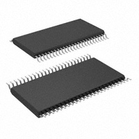


 工商网监
湘ICP备2023018690号
工商网监
湘ICP备2023018690号
