The SN54165 and SN74165 devices
are obsolete and are no longer supplied.
D
D
D
D
SN54165, SN54LS165A, SN74165, SN74LS165A
PARALLEL-LOAD 8-BIT SHIFT REGISTERS
Complementary Outputs
Direct Overriding Load (Data) Inputs
Gated Clock Inputs
Parallel-to-Serial Data Conversion
TYPICAL MAXIMUM
CLOCK FREQUENCY
TYPICAL
POWER DISSIPATION
’165
26 MHz
210 mW
’LS165A
35 MHz
90 mW
TYPE
SDLS062D – OCTOBER 1976 – REVISED FEBRUARY 2002
SN54165, SN54LS165A . . . J OR W PACKAGE
SN74165 . . . N PACKAGE
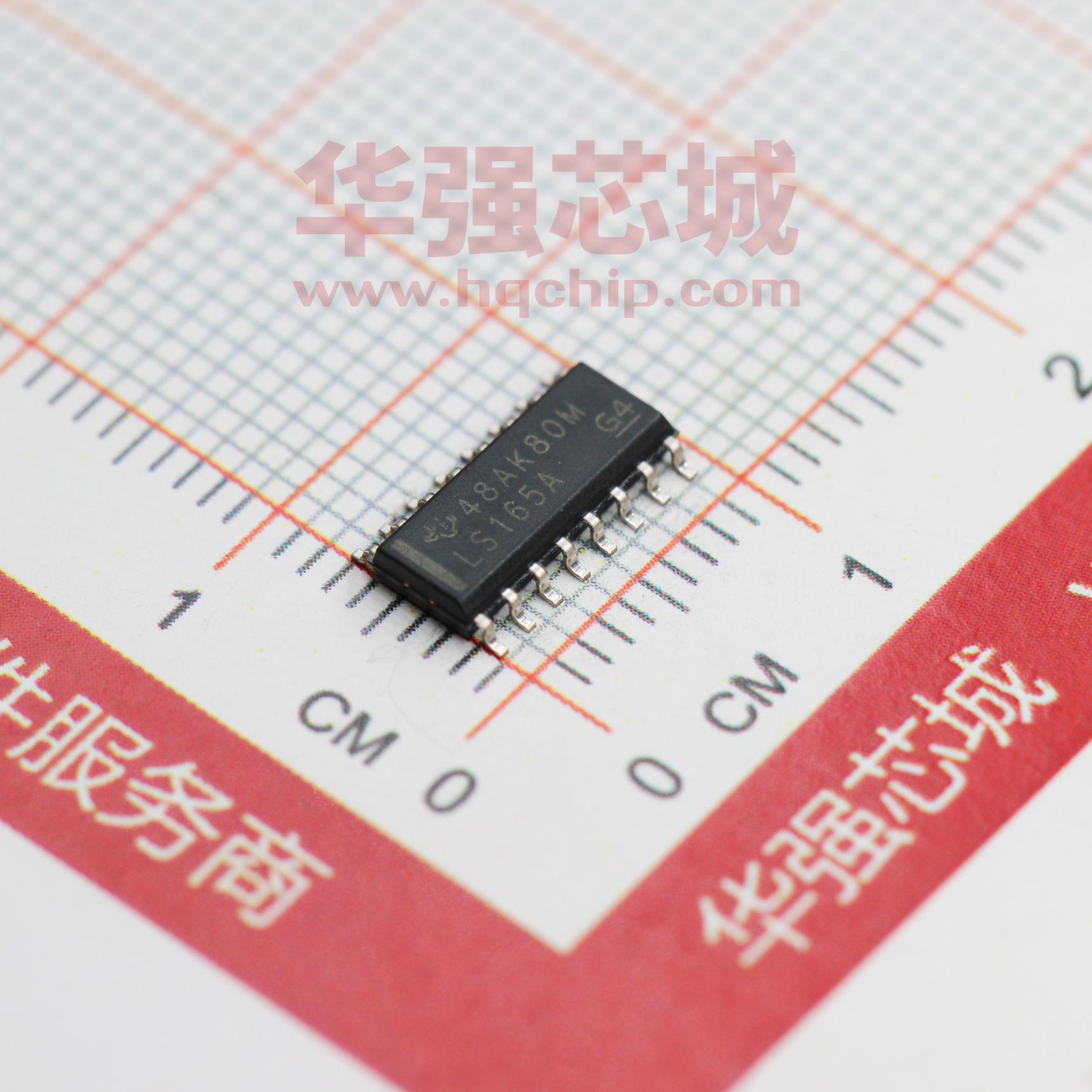
SN74LS165A . . . D, N, OR NS PACKAGE
(TOP VIEW)
SH/LD
CLK
E
F
G
H
QH
GND
description
Clocking is accomplished through a two-input
positive-NOR gate, permitting one input to be
used as a clock-inhibit function. Holding either of
the clock inputs high inhibits clocking, and holding
either clock input low with SH/LD high enables the
other clock input. Clock inhibit (CLK INH) should
be changed to the high level only while CLK is
high. Parallel loading is inhibited as long as SH/LD
is high. Data at the parallel inputs are loaded
directly into the register while SH/LD is low,
independently of the levels of CLK, CLK INH, or
serial (SER) inputs.
16
2
15
3
14
4
13
5
12
6
11
7
10
8
9
VCC
CLK INH
D
C
B
A
SER
QH
CLK
SH/LD
NC
VCC
CLK INH
SN54LS165A . . . FK PACKAGE
(TOP VIEW)
E
F
NC
G
H
4
3 2 1 20 19
18
5
17
6
16
7
15
8
14
9 10 11 12 13
D
C
NC
B
A
QH
GND
NC
QH
SER
The ’165 and ’LS165A are 8-bit serial shift
registers that shift the data in the direction of QA
toward QH when clocked. Parallel-in access to
each stage is made available by eight individual,
direct data inputs that are enabled by a low level
at the shift/load (SH/LD) input. These registers
also feature gated clock (CLK) inputs and
complementary outputs from the eighth bit. All
inputs
are
diode-clamped
to minimize
transmission-line effects, thereby simplifying
system design.
1
NC – No internal connection
Please be aware that an important notice concerning availability, standard warranty, and use in critical applications of
Texas Instruments semiconductor products and disclaimers thereto appears at the end of this data sheet.
Copyright 2002, Texas Instruments Incorporated
PRODUCTION DATA information is current as of publication date.
Products conform to specifications per the terms of Texas Instruments
standard warranty. Production processing does not necessarily include
testing of all parameters.
On products compliant to MIL-PRF-38535, all parameters are tested
unless otherwise noted. On all other products, production
processing does not necessarily include testing of all parameters.
POST OFFICE BOX 655303
• DALLAS, TEXAS 75265
1
�SN54165, SN54LS165A, SN74165, SN74LS165A
PARALLEL-LOAD 8-BIT SHIFT REGISTERS
The SN54165 and SN74165 devices
are obsolete and are no longer supplied.
SDLS062D – OCTOBER 1976 – REVISED FEBRUARY 2002
ORDERING INFORMATION
ORDERABLE
PART NUMBER
PACKAGE†
TA
PDIP – N
0°C to 70°C
Tube
SN74LS165AN
Tube
SN74LS165AD
Tape and reel
SN74LS165ADR
Tape and reel
SN74LS165ANSR
74LS165A
Tube
SN54LS165AJ
SN54LS165AJ
Tube
SNJ54LS165AJ
SNJ54LS165AJ
CFP – W
Tube
SNJ54LS165AW
SNJ54LS165AW
LCCC – FK
Tube
SNJ54LS165AFK
SNJ54LS165AFK
SOIC – D
SOP – NS
CDIP – J
–55°C
55°C to 125°C
TOP-SIDE
MARKING
SN74LS165AN
LS165A
† Package drawings, standard packing quantities, thermal data, symbolization, and PCB design
guidelines are available at www.ti.com/sc/package.
FUNCTION TABLE
INTERNAL
OUTPUTS
INPUTS
2
SH/LD
CLK INH
CLK
SER
PARALLEL
A...H
QA
QB
OUTPUT
QH
L
X
X
X
a...h
a
b
h
H
L
L
X
X
QA0
QB0
QH0
H
L
↑
H
X
H
QAn
QGn
H
L
↑
L
X
L
QAn
QGn
H
H
X
X
X
QA0
QB0
QH0
POST OFFICE BOX 655303
• DALLAS, TEXAS 75265
�The SN54165 and SN74165 devices
are obsolete and are no longer supplied.
SN54165, SN54LS165A, SN74165, SN74LS165A
PARALLEL-LOAD 8-BIT SHIFT REGISTERS
SDLS062D – OCTOBER 1976 – REVISED FEBRUARY 2002
schematics of inputs and outputs
’165
EQUIVALENT OF EACH INPUT
TYPICAL OF BOTH OUTPUTS
VCC
VCC
100 Ω NOM
Req
Input
Output
SH/LD: Req = 3 kΩ NOM
Other Inputs: Req = 6 kΩ NOM
’LS165A
EQUIVALENT OF PARALLEL
INPUTS AND SERIAL INPUT
EQUIVALENT OF ALL
OTHER INPUTS
VCC
Req
TYPICAL OF BOTH OUTPUTS
VCC
120 Ω NOM
24 kΩ NOM
Input
Input
Output
CLK, CLK INH: Req = 10 kΩ NOM
SH/LD: Req = 13 kΩ NOM
POST OFFICE BOX 655303
• DALLAS, TEXAS 75265
3
�SN54165, SN54LS165A, SN74165, SN74LS165A
PARALLEL-LOAD 8-BIT SHIFT REGISTERS
The SN54165 and SN74165 devices
are obsolete and are no longer supplied.
SDLS062D – OCTOBER 1976 – REVISED FEBRUARY 2002
logic diagram (positive logic)
A
SH/LD
CLK INH
CLK
SER
B
11
1
C
12
D
13
E
14
G
F
3
4
H
5
6
15
2
S
C1
1D
R
10
QA
S
C1
1D
R
QB
S
C1
1D
R
QC
S
C1
1D
R
QD
S
C1
1D
R
QE
S
C1
1D
R
S
C1
1D
R
QF
Pin numbers shown are for D, J, N, NS, and W packages.
typical shift, load, and inhibit sequences
CLK
CLK INH
SER
L
SH/LD
Data
Inputs
A
H
B
L
C
H
D
L
E
H
F
L
G
H
H
H
Output QH
H
H
L
H
L
H
L
H
Output QH
L
L
H
L
H
L
H
L
Inhibit
Serial Shift
Load
4
POST OFFICE BOX 655303
• DALLAS, TEXAS 75265
QG
S
C1
1D
R
9
7
QH
QH
�The SN54165 and SN74165 devices
are obsolete and are no longer supplied.
SN54165, SN54LS165A, SN74165, SN74LS165A
PARALLEL-LOAD 8-BIT SHIFT REGISTERS
SDLS062D – OCTOBER 1976 – REVISED FEBRUARY 2002
absolute maximum ratings over operating free-air temperature (unless otherwise noted)†
Supply voltage, VCC (see Note 1) . . . . . . . . . . . . . . . . . . . . . . . . . . . . . . . . . . . . . . . . . . . . . . . . . . . . . . . . . . . . . 7 V
Input voltage, VI: SN54165, SN74165 . . . . . . . . . . . . . . . . . . . . . . . . . . . . . . . . . . . . . . . . . . . . . . . . . . . . . . 5.5 V
SN54LS165A, SN74LS165A . . . . . . . . . . . . . . . . . . . . . . . . . . . . . . . . . . . . . . . . . . . . . . . . . 7 V
Interemitter voltage (see Note 2) . . . . . . . . . . . . . . . . . . . . . . . . . . . . . . . . . . . . . . . . . . . . . . . . . . . . . . . . . . . . 5.5 V
Package thermal impedance θJA (see Note 3): D package . . . . . . . . . . . . . . . . . . . . . . . . . . . . . . . . . . . 73°C/W
N package . . . . . . . . . . . . . . . . . . . . . . . . . . . . . . . . . . . 67°C/W
NS package . . . . . . . . . . . . . . . . . . . . . . . . . . . . . . . . . . 64°C/W
Storage temperature range, Tstg . . . . . . . . . . . . . . . . . . . . . . . . . . . . . . . . . . . . . . . . . . . . . . . . . . . –65°C to 150°C
† Stresses beyond those listed under “absolute maximum ratings” may cause permanent damage to the device. These are stress ratings only, and
functional operation of the device at these or any other conditions beyond those indicated under “recommended operating conditions” is not
implied. Exposure to absolute-maximum-rated conditions for extended periods may affect device reliability.
NOTES: 1. Voltage values, except interemitter voltage, are with respect to network ground terminal.
2. This is the voltage between two emitters of a multiple-emitter transistor. This rating applies for the ’165 to the SH/LD input in
conjunction with the CLK INH input.
3. The package thermal impedance is calculated in accordance with JESD 51-7.
recommended operating conditions
SN54165
SN74165
MIN
NOM
MAX
MIN
NOM
MAX
4.5
5
5.5
4.75
5
5.25
UNIT
VCC
IOH
Supply voltage
High-level output current
–800
–800
mA
IOL
fclock
Low-level output current
16
16
mA
20
MHz
tw(clock)
tw(load)
Width of clock input pulse
25
25
ns
Width of load input pulse
15
15
ns
tsu
tsu
Clock-enable setup time (see Figure 1)
30
30
ns
Parallel input setup time (see Figure 1)
10
10
ns
tsu
tsu
Serial input setup time (see Figure 1)
20
20
ns
Shift setup time (see Figure 1)
45
45
ns
th
TA
Hold time at any input
0
0
ns
Clock frequency
0
Operating free-air temperature
–55
POST OFFICE BOX 655303
• DALLAS, TEXAS 75265
20
125
0
0
70
V
°C
5
�SN54165, SN54LS165A, SN74165, SN74LS165A
PARALLEL-LOAD 8-BIT SHIFT REGISTERS
The SN54165 and SN74165 devices
are obsolete and are no longer supplied.
SDLS062D – OCTOBER 1976 – REVISED FEBRUARY 2002
electrical characteristics over recommended operating free-air temperature range (unless
otherwise noted)
SN54165
TEST CONDITIONS†
PARAMETER
VIH
VIL
High-level input voltage
VIK
Input clamp voltage
VOH
High-level output voltage
VOL
MIN
TYP‡
SN74165
MAX
2
II = –12 mA
VIH = 2 V,
IOH = –800 mA
Low-level output voltage
VCC = MIN,
VIL = 0.8 V,
VIH = 2 V,
IOL = 16 mA
II
Input current at maximum input voltage
VCC = MAX,
VI = 5.5 V
IIH
High level input current
High-level
VCC = MAX
MAX,
4V
VI = 2
2.4
IIL
Low level input current
Low-level
VCC = MAX
MAX,
VI = 0
0.4
4V
IOS
ICC
Supply current
VCC = MAX
VCC = MAX,
See Note 4
SH/LD
Other inputs
SH/LD
Other inputs
Short-circuit output current§
2.4
TYP‡
MAX
2
Low-level input voltage
VCC = MIN,
VCC = MIN,
VIL = 0.8 V,
MIN
–20
V
0.8
0.8
V
–1.5
–1.5
V
3.4
0.2
UNIT
2.4
0.4
3.4
0.2
V
0.4
1
1
80
80
40
40
–3.2
–3.2
–1.6
–1.6
–55
42
–18
63
42
V
mA
µA
mA
–55
mA
63
mA
NOTE 4: With the outputs open, CLK INH and CLK at 4.5 V, and a clock pulse applied to SH/LD, ICC is measured first with the parallel inputs
at 4.5 V, then with the parallel inputs grounded.
† For conditions shown as MIN or MAX, use the appropriate values specified under recommended operating conditions.
‡ All typical values are at VCC = 5 V, TA = 25°C.
§ Not more than one output should be shorted at a time.
SN54165 and SN74165 switching characteristics, VCC = 5 V, TA = 25°C (see Figure 1)
PARAMETER¶
fmax
tPLH
tPHL
tPLH
tPHL
tPLH
tPHL
tPLH
tPHL
FROM
(INPUT)
TO
(OUTPUT)
TEST CONDITIONS
MIN
TYP
20
26
MAX
UNIT
MHz
LD
Any
CL = 15 pF,
pF RL = 400 W
21
31
27
40
CLK
Any
CL = 15 pF,
pF RL = 400 W
16
24
21
31
H
QH
CL = 15 pF,
pF RL = 400 W
H
QH
CL = 15 pF,
pF RL = 400 W
11
17
24
36
18
27
18
27
ns
ns
ns
ns
¶ fmax = maximum clock frequency, tPLH = propagation delay time, low-to-high-level output, tPHL = propagation delay time, high-to-low-level output
6
POST OFFICE BOX 655303
• DALLAS, TEXAS 75265
�The SN54165 and SN74165 devices
are obsolete and are no longer supplied.
SN54165, SN54LS165A, SN74165, SN74LS165A
PARALLEL-LOAD 8-BIT SHIFT REGISTERS
SDLS062D – OCTOBER 1976 – REVISED FEBRUARY 2002
recommended operating conditions
SN54LS165A
VCC
VIH
Supply voltage
VIL
IOH
Low-level input voltage
IOL
fclock
Low-level output current
tw(clock)
( l k)
Width of clock input pulse (see Figure 2)
tw(load)
(l d)
Width of load input pulse
tsu
tsu
High-level input voltage
SN74LS165A
MIN
NOM
MAX
MIN
NOM
MAX
4.5
5
5.5
4.75
5
5.25
2
2
High-level output current
V
V
0.7
0.8
V
–0.4
–0.4
mA
4
Clock frequency
UNIT
0
25
0
8
mA
25
MHz
Clock high
15
15
Clock low
25
25
Clock high
25
25
Clock low
17
17
Clock-enable setup time (see Figure 2)
30
30
ns
Parallel input setup time (see Figure 2)
10
10
ns
tsu
tsu
Serial input setup time (see Figure 2)
20
20
ns
Shift setup time (see Figure 2)
45
45
ns
th
TA
Hold time at any input
0
Operating free-air temperature
ns
ns
0
–55
125
ns
0
70
°C
electrical characteristics over recommended operating free-air temperature range (unless
otherwise noted)
SN54LS165A
TEST CONDITIONS†
PARAMETER
MIN
TYP‡
2.5
3.5
SN74LS165A
MAX
MIN
TYP‡
2.7
3.5
VCC = MIN,
VCC = MIN,
II = –18 mA
VIH = 2 V,
VIL = MAX,
VOL
VCC = MIN
MIN,
VIH = 2 V
V,
II
IIH
VCC = MAX,
VCC = MAX,
VI = 7 V
VI = 2.7 V
0.1
0.1
20
20
µA
IIL
IOS§
VCC = MAX,
VCC = MAX
VI = 0.4 V
–0.4
–0.4
mA
–100
mA
IOH = –0.4 mA
IOL = 4 mA
0.25
–1.5
UNIT
VIK
VOH
VIL = MAX
–1.5
MAX
0.4
IOL = 8 mA
–20
–100
–20
V
V
0.25
0.4
0.35
0.5
V
mA
ICC
VCC = MAX, See Note 4
18
30
18
30
mA
NOTE 4. With the outputs open, CLK INH and CLK at 4.5 V, and a clock pulse applied to SH/LD, ICC is measured first with the parallel inputs
at 4.5 V, then with the parallel inputs grounded.
† For conditions shown as MIN or MAX, use the appropriate values specified under recommended operating conditions.
‡ All typical values are at VCC = 5 V, TA = 25°C.
§ Not more than one output should be shorted at a time, and the duration of the short-circuit should not exceed one second.
POST OFFICE BOX 655303
• DALLAS, TEXAS 75265
7
�SN54165, SN54LS165A, SN74165, SN74LS165A
PARALLEL-LOAD 8-BIT SHIFT REGISTERS
SDLS062D – OCTOBER 1976 – REVISED FEBRUARY 2002
The SN54165 and SN74165 devices
are obsolete and are no longer supplied.
SN54LS165A and SN74LS165A switching characteristics, VCC = 5 V, TA = 25°C (see Figure 2)
PARAMETER†
fmax
tPLH
tPHL
tPLH
tPHL
tPLH
tPHL
tPLH
tPHL
FROM
(INPUT)
TO
(OUTPUT)
TEST CONDITIONS
MIN
TYP
25
35
MAX
UNIT
MHz
LD
Any
RL = 2 kW, CL = 15 pF
21
35
26
35
CLK
Any
RL = 2 kW, CL = 15 pF
14
25
16
25
H
QH
RL = 2 kW, CL = 15 pF
13
25
24
30
H
QH
RL = 2 kW, CL = 15 pF
19
30
17
25
ns
ns
ns
ns
† fmax = maximum clock frequency, tPLH = propagation delay time, low-to-high-level output, tPHL = propagation delay time, high-to-low-level output
8
POST OFFICE BOX 655303
• DALLAS, TEXAS 75265
�The SN54165 and SN74165 devices
are obsolete and are no longer supplied.
SN54165, SN54LS165A, SN74165, SN74LS165A
PARALLEL-LOAD 8-BIT SHIFT REGISTERS
SDLS062D – OCTOBER 1976 – REVISED FEBRUARY 2002
PARAMETER MEASUREMENT INFORMATION
SERIES 54/74 DEVICES
VCC
Test
Point
VCC
RL
(see Note B)
From Output
Under Test
CL
(see Note A)
High-Level
Pulse
1.5 V
S2
LOAD CIRCUIT
FOR 3-STATE OUTPUTS
3V
Timing
Input
1.5 V
1 kΩ
Test
Point
LOAD CIRCUIT
FOR OPEN-COLLECTOR OUTPUTS
LOAD CIRCUIT
FOR 2-STATE TOTEM-POLE OUTPUTS
S1
(see Note B)
CL
(see Note A)
RL
CL
(see Note A)
RL
From Output
Under Test
VCC
From Output
Under Test
Test
Point
1.5 V
0V
tw
Low-Level
Pulse
1.5 V
tsu
0V
In-Phase
Output
(see Note D)
tPHL
VOH
1.5 V
Out-of-Phase
Output
(see Note D)
1.5 V
3V
1.5 V
Waveform 1
(see Notes C
and D)
tPLZ
VOH
1.5 V
1.5 V
VOL
VOL
Waveform 2
(see Notes C
and D)
VOLTAGE WAVEFORMS
PROPAGATION DELAY TIMES
≈1.5 V
1.5 V
tPZH
tPLH
1.5 V
0V
tPZL
VOL
tPHL
1.5 V
0V
Output
Control
(low-level
enabling)
1.5 V
tPLH
1.5 V
VOLTAGE WAVEFORMS
SETUP AND HOLD TIMES
3V
1.5 V
3V
Data
Input
1.5 V
VOLTAGE WAVEFORMS
PULSE DURATIONS
Input
th
VOL + 0.5 V
tPHZ
VOH
1.5 V
VOH – 0.5 V
≈1.5 V
VOLTAGE WAVEFORMS
ENABLE AND DISABLE TIMES, 3-STATE OUTPUTS
NOTES: A. CL includes probe and jig capacitance.
B. All diodes are 1N3064 or equivalent.
C. Waveform 1 is for an output with internal conditions such that the output is low except when disabled by the output control.
Waveform 2 is for an output with internal conditions such that the output is high except when disabled by the output control.
D. S1 and S2 are closed for tPLH, tPHL, tPHZ, and tPLZ; S1 is open and S2 is closed for tPZH; S1 is closed and S2 is open for tPZL.
E. All input pulses are supplied by generators having the following characteristics: PRR ≤ 1 MHz, ZO ≈ 50 Ω; tr and tf ≤ 7 ns for Series
54/74 devices and tr and tf ≤ 2.5 ns for Series 54S/74S devices.
F. The outputs are measured one at a time with one input transition per measurement.
Figure 1. Load Circuits and Voltage Waveforms
POST OFFICE BOX 655303
• DALLAS, TEXAS 75265
9
�SN54165, SN54LS165A, SN74165, SN74LS165A
PARALLEL-LOAD 8-BIT SHIFT REGISTERS
The SN54165 and SN74165 devices
are obsolete and are no longer supplied.
SDLS062D – OCTOBER 1976 – REVISED FEBRUARY 2002
PARAMETER MEASUREMENT INFORMATION
SERIES 54LS/74LS DEVICES
VCC
Test
Point
VCC
RL
From Output
Under Test
CL
(see Note A)
CL
(see Note A)
High-Level
Pulse
1.3 V
S2
LOAD CIRCUIT
FOR 3-STATE OUTPUTS
3V
Timing
Input
1.3 V
5 kΩ
Test
Point
LOAD CIRCUIT
FOR OPEN-COLLECTOR OUTPUTS
LOAD CIRCUIT
FOR 2-STATE TOTEM-POLE OUTPUTS
S1
(see Note B)
CL
(see Note A)
RL
(see Note B)
RL
From Output
Under Test
VCC
From Output
Under Test
Test
Point
1.3 V
0V
tw
Low-Level
Pulse
1.3 V
tsu
Data
Input
1.3 V
VOLTAGE WAVEFORMS
PULSE DURATIONS
1.3 V
1.3 V
Output
Control
(low-level
enabling)
0V
tPLH
In-Phase
Output
(see Note D)
1.3 V
0V
3V
1.3 V
1.3 V
0V
tPZL
tPLZ
tPHL
VOH
1.3 V
1.3 V
Waveform 1
(see Notes C
and D)
VOL
tPZH
tPLH
VOH
1.3 V
1.3 V
VOL
VOLTAGE WAVEFORMS
PROPAGATION DELAY TIMES
≈1.5 V
1.3 V
VOL
tPHL
Out-of-Phase
Output
(see Note D)
3V
1.3 V
VOLTAGE WAVEFORMS
SETUP AND HOLD TIMES
3V
Input
th
Waveform 2
(see Notes C
and D)
VOL + 0.5 V
tPHZ
VOH
1.3 V
VOH – 0.5 V
≈1.5 V
VOLTAGE WAVEFORMS
ENABLE AND DISABLE TIMES, 3-STATE OUTPUTS
NOTES: A. CL includes probe and jig capacitance.
B. All diodes are 1N3064 or equivalent.
C. Waveform 1 is for an output with internal conditions such that the output is low except when disabled by the output control.
Waveform 2 is for an output with internal conditions such that the output is high except when disabled by the output control.
D. S1 and S2 are closed for tPLH, tPHL, tPHZ, and tPLZ; S1 is open and S2 is closed for tPZH; S1 is closed and S2 is open for tPZL.
E. Phase relationships between inputs and outputs have been chosen arbitrarily for these examples.
F. All input pulses are supplied by generators having the following characteristics: PRR ≤ 1 MHz, ZO ≈ 50 Ω, tr ≤ 1.5 ns, tf ≤ 2.6 ns.
G. The outputs are measured one at a time with one input transition per measurement.
Figure 2. Load Circuits and Voltage Waveforms
10
POST OFFICE BOX 655303
• DALLAS, TEXAS 75265
�PACKAGE OPTION ADDENDUM
www.ti.com
24-Aug-2018
PACKAGING INFORMATION
Orderable Device
Status
(1)
Package Type Package Pins Package
Drawing
Qty
Eco Plan
Lead/Ball Finish
MSL Peak Temp
(2)
(6)
(3)
Op Temp (°C)
Device Marking
(4/5)
5962-7700601VEA
ACTIVE
CDIP
J
16
1
TBD
A42
N / A for Pkg Type
-55 to 125
5962-7700601VE
A
SNV54LS165AJ
5962-7700601VFA
ACTIVE
CFP
W
16
1
TBD
A42
N / A for Pkg Type
-55 to 125
5962-7700601VF
A
SNV54LS165AW
7700601EA
ACTIVE
CDIP
J
16
1
TBD
A42
N / A for Pkg Type
-55 to 125
7700601EA
SNJ54LS165AJ
7700601FA
ACTIVE
CFP
W
16
1
TBD
A42
N / A for Pkg Type
-55 to 125
7700601FA
SNJ54LS165AW
JM38510/30608B2A
ACTIVE
LCCC
FK
20
1
TBD
POST-PLATE
N / A for Pkg Type
-55 to 125
JM38510/
30608B2A
JM38510/30608BEA
ACTIVE
CDIP
J
16
1
TBD
A42
N / A for Pkg Type
-55 to 125
JM38510/
30608BEA
JM38510/30608BFA
ACTIVE
CFP
W
16
1
TBD
A42
N / A for Pkg Type
-55 to 125
JM38510/
30608BFA
M38510/30608B2A
ACTIVE
LCCC
FK
20
1
TBD
POST-PLATE
N / A for Pkg Type
-55 to 125
JM38510/
30608B2A
M38510/30608BEA
ACTIVE
CDIP
J
16
1
TBD
A42
N / A for Pkg Type
-55 to 125
JM38510/
30608BEA
M38510/30608BFA
ACTIVE
CFP
W
16
1
TBD
A42
N / A for Pkg Type
-55 to 125
JM38510/
30608BFA
SN54LS165AJ
ACTIVE
CDIP
J
16
1
TBD
A42
N / A for Pkg Type
-55 to 125
SN54LS165AJ
SN74LS165AD
ACTIVE
SOIC
D
16
40
Green (RoHS
& no Sb/Br)
CU NIPDAU
Level-1-260C-UNLIM
0 to 70
LS165A
SN74LS165ADR
ACTIVE
SOIC
D
16
2500
Green (RoHS
& no Sb/Br)
CU NIPDAU
Level-1-260C-UNLIM
0 to 70
LS165A
SN74LS165AN
ACTIVE
PDIP
N
16
25
Green (RoHS
& no Sb/Br)
CU NIPDAU
N / A for Pkg Type
0 to 70
SN74LS165AN
SN74LS165ANE4
ACTIVE
PDIP
N
16
25
Green (RoHS
& no Sb/Br)
CU NIPDAU
N / A for Pkg Type
0 to 70
SN74LS165AN
SN74LS165ANSR
ACTIVE
SO
NS
16
2000
Green (RoHS
& no Sb/Br)
CU NIPDAU
Level-1-260C-UNLIM
0 to 70
74LS165A
Addendum-Page 1
Samples
�PACKAGE OPTION ADDENDUM
www.ti.com
Orderable Device
24-Aug-2018
Status
(1)
Package Type Package Pins Package
Drawing
Qty
Eco Plan
Lead/Ball Finish
MSL Peak Temp
(2)
(6)
(3)
Op Temp (°C)
Device Marking
(4/5)
SNJ54LS165AFK
ACTIVE
LCCC
FK
20
1
TBD
POST-PLATE
N / A for Pkg Type
-55 to 125
SNJ54LS
165AFK
SNJ54LS165AJ
ACTIVE
CDIP
J
16
1
TBD
A42
N / A for Pkg Type
-55 to 125
7700601EA
SNJ54LS165AJ
SNJ54LS165AW
ACTIVE
CFP
W
16
1
TBD
A42
N / A for Pkg Type
-55 to 125
7700601FA
SNJ54LS165AW
(1)
The marketing status values are defined as follows:
ACTIVE: Product device recommended for new designs.
LIFEBUY: TI has announced that the device will be discontinued, and a lifetime-buy period is in effect.
NRND: Not recommended for new designs. Device is in production to support existing customers, but TI does not recommend using this part in a new design.
PREVIEW: Device has been announced but is not in production. Samples may or may not be available.
OBSOLETE: TI has discontinued the production of the device.
(2)
RoHS: TI defines "RoHS" to mean semiconductor products that are compliant with the current EU RoHS requirements for all 10 RoHS substances, including the requirement that RoHS substance
do not exceed 0.1% by weight in homogeneous materials. Where designed to be soldered at high temperatures, "RoHS" products are suitable for use in specified lead-free processes. TI may
reference these types of products as "Pb-Free".
RoHS Exempt: TI defines "RoHS Exempt" to mean products that contain lead but are compliant with EU RoHS pursuant to a specific EU RoHS exemption.
Green: TI defines "Green" to mean the content of Chlorine (Cl) and Bromine (Br) based flame retardants meet JS709B low halogen requirements of


 工商网监
湘ICP备2023018690号
工商网监
湘ICP备2023018690号

