SN74LV165A
SCLS402P – APRIL 1998 – REVISED JUNE 2022
SN74LV165A Parallel-Load 8-Bit Shift Registers
1 Features
3 Description
•
•
•
The SN74LV165A device is a parallel-load, 8-bit shift
registers designed for 2 V to 5.5 V VCC operation.
•
When the device is clocked, data is shifted toward the
serial output QH. Parallel-in access to each stage is
provided by eight individual direct data inputs that are
enabled by a low level at the shift/load (SH/ LD) input.
The ’LV165A devices feature a clock-inhibit function
and a complemented serial output, Q H.
2 Applications
•
This device is fully specified for partial-power-down
applications using Ioff. The Ioff circuitry disables
the outputs, preventing damaging current backflow
through the devices when they are powered down.
Increase the Number of Inputs on a Microcontroller
Device Information(1)
PART NUMBER
SN74LV165A
PACKAGE
D (SOIC, 16)
9.90 mm × 3.90 mm
DB (SSOP, 16)
6.20 mm × 5.30 mm
NS (SO, 16)
10.20 mm × 5.30 mm
PW (TSSOP, 16)
5.00 mm × 4.40 mm
DGV (TVSOP, 16)
3.60 mm × 4.40 mm
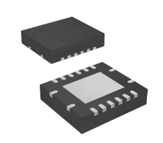
RGY (VQFN, 16)
4.00 mm × 3.50 mm
BQB (WQFN,
(1)
(2)
A
B
C
BODY SIZE (NOM)
16)(2)
3.60 mm × 2.60 mm
For all available packages, see the orderable addendum at
the end of the data sheet.
Preview
D
E
F
G
H
SH/LD
5 Additional
Shift Register
Stages
SER
S
R
S
R
S
R
D
Q
D
Q
D
Q
QH
Q
QH
CLK INH
CLK
Logic Diagram (Positive Logic)
An IMPORTANT NOTICE at the end of this data sheet addresses availability, warranty, changes, use in safety-critical applications,
intellectual property matters and other important disclaimers. ADVANCE INFORMATION for preproduction products; subject to change
without notice.
ADVANCE INFORMATION
•
2 V to 5.5 V VCC operation
Maximum tpd of 10.5 ns at 5 V
Support mixed-mode voltage operation on
all ports
Ioff supports partial-power-down mode
operation
Latch-up performance exceeds 250 mA per
JESD 17
�SN74LV165A
www.ti.com
SCLS402P – APRIL 1998 – REVISED JUNE 2022
Table of Contents
ADVANCE INFORMATION
1 Features............................................................................1
2 Applications..................................................................... 1
3 Description.......................................................................1
4 Revision History.............................................................. 2
5 Pin Configuration and Functions...................................3
6 Specifications.................................................................. 4
6.1 Absolute Maximum Ratings........................................ 4
6.2 ESD Ratings............................................................... 4
6.3 Recommended Operating Conditions.........................5
6.4 Thermal Information....................................................5
6.5 Electrical Characteristics.............................................6
6.6 Timing Requirements, VCC = 2.5 V ± 0.2 V.................6
6.7 Timing Requirements, VCC = 3.3 V ± 0.3 V.................6
6.8 Timing Requirements, VCC = 5 V ± 0.5 V....................7
6.9 Switching Characteristics, VCC = 2.5 V ± 0.2 V...........8
6.10 Switching Characteristics, VCC = 3.3 V ± 0.3 V.........8
6.11 Switching Characteristics,VCC = 5 V ± 0.5 V............. 8
6.12 Operating Characteristics......................................... 8
6.13 Typical Characteristics.............................................. 9
7 Parameter Measurement Information.......................... 10
8 Detailed Description...................................................... 11
8.1 Overview................................................................... 11
8.2 Functional Block Diagram......................................... 11
8.3 Feature Description...................................................11
8.4 Device Functional Modes..........................................13
9 Application and Implementation.................................. 14
9.1 Application Information............................................. 14
9.2 Typical Application.................................................... 14
10 Power Supply Recommendations..............................17
11 Layout........................................................................... 17
11.1 Layout Guidelines................................................... 17
11.2 Layout Example...................................................... 17
12 Device and Documentation Support..........................18
12.1 Related Documentation.......................................... 18
12.2 Related Links.......................................................... 18
12.3 Receiving Notification of Documentation Updates..18
12.4 Support Resources................................................. 18
12.5 Trademarks............................................................. 18
12.6 Electrostatic Discharge Caution..............................18
12.7 Glossary..................................................................18
13 Mechanical, Packaging, and Orderable
Information.................................................................... 18
4 Revision History
NOTE: Page numbers for previous revisions may differ from page numbers in the current version.
Changes from Revision O (November 2016) to Revision P (June 2022)
Page
• Updated the numbering format for tables, figures, and cross-references throughout the document..................1
• Added BQB (WQFN) package information to Device Information, Pin Configuration and Thermal Information
tables.................................................................................................................................................................. 1
• Updated specifications table formatting..............................................................................................................6
Changes from Revision N (July 2013) to Revision O (November 2016)
Page
• Added Applications section, Device Information table, Table of Contents, Pin Configuration and Functions
section, Specifications section, ESD Ratings table, Thermal Information table, Typical Characteristics section,
Detailed Description section, Application and Implementation section, Power Supply Recommendations
section, Layout section, Device and Documentation Support section, and Mechanical, Packaging, and
Orderable Information section ........................................................................................................................... 1
2
Submit Document Feedback
Copyright © 2022 Texas Instruments Incorporated
Product Folder Links: SN74LV165A
�SN74LV165A
www.ti.com
SCLS402P – APRIL 1998 – REVISED JUNE 2022
5 Pin Configuration and Functions
SH/LD VCC
1
16
2
15
3
14
4
13
5
12
6
11
7
10
8
9
VCC
CLK INH
D
C
B
A
SER
QH
1
Figure 5-1. D, DB, DGV, N or PW Package
16-Pin SOIC, SSOP, TVSOP, SOP or TSSOP
Top View
16
CLK
2
15
E
3
F
4
14
13
G
5
H
6
11
A
QH
7
10
SER
PAD
12
8
9
GND
QH
CLK INH
D
C
B
Figure 5-2. RGY or BQB Package
16-Pin VQFN or WQFN
Top View
ADVANCE INFORMATION
SH/LD
CLK
E
F
G
H
QH
GND
Table 5-1. Pin Functions
PIN
NAME
NO.
TYPE (1)
DESCRIPTION
A
11
I
Serial input A
B
12
I
Serial input B
C
13
I
Serial input C
CLK
2
I
Storage clock
CLK INH
15
I
Storage clock
D
14
I
Serial input D
E
3
I
Serial input E
F
4
I
Serial input F
G
5
I
Serial input G
GND
8
G
Ground pin
H
6
I
Serial input H
QH
7
O
Output H, inverted
QH
9
O
Output H
SH/ LD
1
I
Load Input
SER
10
I
Serial input
VCC
16
P
Power pin
PAD
-
-
Thermal Pad(2)
(1)
(2)
I = Input, O = Output, I/O = Input or Output, G = Ground, P = Power.
RGY and BQB Package Only
Submit Document Feedback
Copyright © 2022 Texas Instruments Incorporated
Product Folder Links: SN74LV165A
3
�SN74LV165A
www.ti.com
SCLS402P – APRIL 1998 – REVISED JUNE 2022
6 Specifications
6.1 Absolute Maximum Ratings
over operating free-air temperature range (unless otherwise noted)(1)
MIN
MAX
UNIT
Supply voltage
–0.5
7
V
voltage(2)
–0.5
7
V
–0.5
7
V
–0.5
Input
Voltage range applied to any output in the high-impedance or power-off state(2)
Output voltage
(2) (3)
VCC + 0.5
V
Input clamp current
VI < 0
–20
mA
Output clamp current
VO < 0
–50
mA
Continuous output current
VO = 0 to VCC
±25
mA
ADVANCE INFORMATION
Continuous current through VCC or GND
±50
mA
Tjmax
Maximum virtual junction temperature
150
°C
Tstg
Storage temperature
150
°C
(1)
(2)
(3)
–65
Stresses beyond those listed under Absolute Maximum Ratings may cause permanent damage to the device. These are stress
ratings only, which do not imply functional operation of the device at these or any other conditions beyond those indicated under
Recommended Operating Conditions. Exposure to absolute-maximum-rated conditions for extended periods may affect device
reliability.
The input and output negative-voltage ratings may be exceeded if the input and output current ratings are observed.
This value is limited to 5.5 V maximum.
6.2 ESD Ratings
VALUE
Human-body model (HBM), per ANSI/ESDA/JEDEC JS-001 (1)
V(ESD)
(1)
(2)
4
Electrostatic discharge
UNIT
±2000
Machine Model (MM), per JEDEC specification
±200
Charged-device model (CDM), per ANSI/ESDA/JEDEC JS-002 (2)
±1000
V
JEDEC document JEP155 states that 500-V HBM allows safe manufacturing with a standard ESD control process.
JEDEC document JEP157 states that 250-V CDM allows safe manufacturing with a standard ESD control process.
Submit Document Feedback
Copyright © 2022 Texas Instruments Incorporated
Product Folder Links: SN74LV165A
�SN74LV165A
www.ti.com
SCLS402P – APRIL 1998 – REVISED JUNE 2022
6.3 Recommended Operating Conditions
over operating free-air temperature range (unless otherwise noted)(1)
MAX
2
5.5
Supply voltage
VCC = 2 V
VIH
High-level input voltage
UNIT
V
1.5
VCC = 2.3 V to 2.7 V
VCC × 0.7
VCC = 3 V to 3.6 V
VCC × 0.7
VCC = 4.5 V to 5.5 V
VCC × 0.7
V
VCC = 2 V
0.5
VCC = 2.3 V to 2.7 V
VCC × 0.3
VCC = 3 V to 3.6 V
VCC × 0.3
VIL
Low-level input voltage
VI
Input voltage
0
5.5
V
VO
Output voltage
0
VCC
V
–50
µA
VCC = 4.5 V to 5.5 V
VCC × 0.3
VCC = 2 V
IOH
VCC = 2.3 V to 2.7 V
High-level output current
–2
VCC = 3 V to 3.6 V
–6
VCC = 4.5 V to 5.5 V
Δt/Δv
50
VCC = 2.3 V to 2.7 V
Low-level output current
6
VCC = 4.5 V to 5.5 V
12
VCC = 2.3 V to 2.7 V
200
VCC = 3 V to 3.6 V
100
VCC = 4.5 V to 5.5 V
TA
(1)
Operating free-air temperature
µA
2
VCC = 3 V to 3.6 V
Input transition rise or fall rate
mA
–12
VCC = 2 V
IOL
V
ADVANCE INFORMATION
VCC
MIN
mA
ns/V
20
SN54LV165A
–55
125
SN74LV165A
–40
125
°C
All unused inputs of the device must be held at VCC or GND to ensure proper device operation. See Implications of Slow or Floating
CMOS Inputs
6.4 Thermal Information
SN74LV165A
THERMAL METRIC(1)
D
(SOIC)
DB
(SSOP)
NS
(SO)
PW
(TSSOP)
DGV
(TVSOP)
RGY
(VQFN)
BQB
(WQFN)
16 PINS
16 PINS
16 PINS
16 PINS
16 PINS
16 PINS
16 PINS
UNIT
RθJA
Junction-to-ambient thermal
resistance
86.2
102.8
89.4
113.3
125.9
48.8
85.9
°C/W
RθJC(top)
Junction-to-case (top) thermal
resistance
46.1
53.3
47.9
48.3
51
46.7
82.4
°C/W
RθJB
Junction-to-board thermal
resistance
43.8
53.5
49.8
58.4
57.7
24.9
55.6
°C/W
ψJT
Junction-to-top characterization
parameter
13.2
16.6
16.6
6.4
5.7
2
9.4
°C/W
ψJB
Junction-to-board
characterization parameter
43.5
52.9
49.5
57.8
57.2
24.9
55.6
°C/W
RθJC(bot)
Junction-to-case (bottom) thermal
resistance
N/A
N/A
N/A
N/A
N/A
11.7
33.3
°C/W
(1)
For more information about traditional and new thermal metrics, see Semiconductor and IC Package Thermal Metrics
Submit Document Feedback
Copyright © 2022 Texas Instruments Incorporated
Product Folder Links: SN74LV165A
5
�SN74LV165A
www.ti.com
SCLS402P – APRIL 1998 – REVISED JUNE 2022
6.5 Electrical Characteristics
over operating free-air temperature range (unless otherwise noted).
PARAMETER
VOH
TEST CONDITIONS
High-level output
voltage
VCC
–40°C to 85°C
–40°C to 125°C
–55°C to 125°C
MIN
MIN
MIN
TYP MAX
VCC –
0.1
TYP MAX
VCC –
0.1
TYP MAX
VCC –
0.1
IOH = –50 mA
2 V to 5.5 V
IOH = –2 mA
2.3 V
2
2
2
IOH = –6 mA
3V
2.48
2.48
2.48
4.5 V
3.8
IOH = –12 mA
3.8
V
3.8
ADVANCE INFORMATION
IOL = 50 mA
2 V to 5.5 V
IOL = 2 mA
2.3 V
0.4
0.4
0.4
IOL = 6 mA
3V
0.44
0.44
0.44
4.5 V
VOL
Low-level output voltage
II
Input leakage current
VI = 5.5 V or GND
ICC
Static supply current
VI = VCC or GND, IO = 0
Ioff
Partial power down
current
VI or VO = 0 to 5.5 V
Ci
Input capacitance
VI = VCC or GND
IOL = 12 mA
UNIT
0.1
0.1
0.1
V
0.55
0.55
0.55
0 V to 5.5 V
±1
±1
±1
µA
5.5 V
20
20
20
µA
0
5
5
5
µA
3.3 V
1.7
1.7
1.7
pF
6.6 Timing Requirements, VCC = 2.5 V ± 0.2 V
over recommended operating free-air temperature range (unless otherwise noted) (see Figure 7-1)
PARAMETER
tw
Pulse duration
TEST CONDITION
25°C
MIN
CLK high or low
SH/ LD low
th
Setup time
Hold time
–40°C to 85°C
MIN
MAX
–40°C to 125°C
MIN
MAX
–55°C to 125°C
MIN
MAX
8.5
9
9
9
11
13
13
13
SH/ LD high before CLK↑
tsu
MAX
7
8.5
8.5
8.5
8.5
9.5
9.5
9.5
7
7
7
7
Data before SH/ LD↑
11.5
12
12
12
SER data after CLK↑
SER before CLK↑
CLK INH before CLK↑
-1
0
0
0
Parallel data after SH/ LD↑
0
0
0
0
SH/ LD high after CLK↑
0
0
0
0
UNIT
ns
ns
ns
6.7 Timing Requirements, VCC = 3.3 V ± 0.3 V
over recommended operating free-air temperature range (unless otherwise noted (see Figure 7-1)
PARAMETER
tw
tsu
th
Pulse duration
Setup time
Hold time
TEST CONDITION
CLK high or low
MAX
–40°C to 85°C
MIN
MAX
–40°C to 125°C
MIN
MAX
–55°C to 125°C
MIN
MAX
6
7
7
7
7.5
9
9
9
SH/ LD high before CLK↑
5
6
6
6
SER before CLK↑
5
6
6
6
CLK INH before CLK↑
5
5
5
5
Data before SH/ LD↑
7.5
8.5
8.5
8.5
SER data after CLK↑
0
0
0
0
0.5
0.5
0.5
0.5
0
0
0
0
SH/ LD low
Parallel data after SH/ LD↑
SH/ LD high after CLK↑
6
25°C
MIN
Submit Document Feedback
UNIT
ns
ns
ns
Copyright © 2022 Texas Instruments Incorporated
Product Folder Links: SN74LV165A
�SN74LV165A
www.ti.com
SCLS402P – APRIL 1998 – REVISED JUNE 2022
6.8 Timing Requirements, VCC = 5 V ± 0.5 V
over recommended operating free-air temperature range (unless otherwise noted) (see Figure 7-1)
tw
tsu
th
Pulse duration
Setup time
Hold time
25°C
TEST CONDITION
MIN
–40°C to 85°C
MAX
MIN
–40°C to 125°C
MAX
MIN
MAX
–55°C to 125°C
MIN
MAX
CLK high or low
4
4
4
4
SH/ LD low
5
6
6
5
SH/ LD high before CLK↑
4
4
4
4
SER before CLK↑
4
4
4
4
3.5
3.5
3.5
3.5
CLK INH before CLK↑
Data before SH/ LD↑
5
5
5
5
SER data after CLK↑
0.5
0.5
0.5
0.5
Parallel data after SH/ LD↑
SH/ LD high after CLK↑
1
1
1
1
0.5
0.5
0.5
0.5
UNIT
ns
ns
ns
ADVANCE INFORMATION
PARAMETER
CLK
CLK INH
SER
L
SH/LD
Data
Inputs
A
H
B
L
C
H
D
L
E
H
F
L
G
H
H
H
QH
H
H
L
H
L
H
L
H
QH
L
L
H
L
H
L
H
L
Inhibit
Serial Shift
Load
Figure 6-1. Typical Shift, Load, and Inhibit Sequences
Submit Document Feedback
Copyright © 2022 Texas Instruments Incorporated
Product Folder Links: SN74LV165A
7
�SN74LV165A
www.ti.com
SCLS402P – APRIL 1998 – REVISED JUNE 2022
6.9 Switching Characteristics, VCC = 2.5 V ± 0.2 V
over operating free-air temperature range (unless otherwise noted), (see Figure 7-1)
PARAM
ETER
FROM
(INPUT)
TO
(OUTPUT)
fmax
LOAD
CAP
25°C
MIN
SH/ LD
QH or Q
QH or Q
TYP MAX
MIN
TYP MAX
MIN
80
45
45
45
CL = 50 pF
40
65
35
35
35
CL = 15 pF
CLK
SH/ LD
MIN
–55°C to 125°C
50
H
tpd
TYP MAX
–40°C to 125°C
CL = 15 pF
CLK
tpd
–40°C to 85°C
CL = 50 pF
ADVANCE INFORMATION
H
TYP MAX
UNIT
MHz
12.2
19.8
1
22
1
22
1
22
13.1
21.5
1
23.5
1
23.5
1
23.5
12.9
21.7
1
24
1
24
1
24
15.3
23.3
1
26
1
26
1
26
16.1
25.1
1
28
1
28
1
28
15.9
25.3
1
28
1
28
1
28
ns
ns
6.10 Switching Characteristics, VCC = 3.3 V ± 0.3 V
over operating free-air temperature range (unless otherwise noted), (see Figure 7-1)
PARAM
ETER
FROM
(INPUT)
TO
(OUTPUT)
fmax
LOAD
CAP
25°C
MIN
SH/ LD
QH or Q
QH or Q
–40°C to 125°C
MIN
–55°C to 125°C
TYP MAX
MIN
65
115
55
55
55
60
90
50
50
50
CL = 15 pF
CLK
SH/ LD
TYP MAX
CL = 50 pF
H
tpd
MIN
CL = 15 pF
CLK
tpd
–40°C to 85°C
TYP MAX
CL = 50 pF
H
TYP MAX
UNIT
MHz
8.6
15.4
1
18
1
18
1
18
9.1
15.8
1
18.5
1
18.5
1
18.5
8.9
14.1
1
16.5
1
16.5
1
16.5
10.9
14.9
1
16.9
1
16.9
1
16.9
11.3
19.3
1
22
1
22
1
22
11.1
17.6
1
20
1
20
1
20
ns
ns
6.11 Switching Characteristics,VCC = 5 V ± 0.5 V
over recommended operating free-air temperature range (see Figure 7-1)
PARAM
ETER
FROM
(INPUT)
TO
(OUTPUT)
fmax
LOAD
CAP
SH/ LD
QH or Q
QH or Q
TYP MAX
–40°C to 125°C
MIN
110
165
90
90
95
125
85
85
CL = 15 pF
H
SH/ LD
MIN
CL = 50 pF
CLK
tpd
–40°C to 85°C
TYP MAX
CL = 15 pF
CLK
tpd
25°C
MIN
CL = 50 pF
H
–55°C to 125°C
TYP MAX
MIN
TYP MAX
90
UNIT
MHz
6
9.9
1
11.5
1
11.5
1
11.5
6
9.9
1
11.5
1
11.5
1
11.5
6
9.9
1
10.5
1
10.5
1
10.5
7.7
11.9
1
13.5
1
13.5
1
13.5
7.7
11.9
1
13.5
1
13.5
1
13.5
7.6
11
1
12.5
1
12.5
1
12.5
ns
ns
6.12 Operating Characteristics
TA = 25°C
PARAMETER
Cpd
8
Power dissipation capacitance
TEST CONDITIONS
CL = 50 pF
Submit Document Feedback
f = 10 MHz
VCC
TYP
3.3 V
36.1
5V
37.5
UNIT
pF
Copyright © 2022 Texas Instruments Incorporated
Product Folder Links: SN74LV165A
�SN74LV165A
www.ti.com
SCLS402P – APRIL 1998 – REVISED JUNE 2022
6.13 Typical Characteristics
16
CL=15pF
CL=50pF
15
14
Tpd typ (ns)
13
12
11
10
9
8
6
2.5
2.75
3
3.25
3.5
3.75 4
Vcc(V)
4.25
4.5
4.75
ADVANCE INFORMATION
7
5
D001
Figure 6-2. TPD Typical (25°C) vs Vcc
Submit Document Feedback
Copyright © 2022 Texas Instruments Incorporated
Product Folder Links: SN74LV165A
9
�SN74LV165A
www.ti.com
SCLS402P – APRIL 1998 – REVISED JUNE 2022
7 Parameter Measurement Information
7.1
VCC
Test
Point
From Output
Under Test
RL = 1 kΩ
From Output
Under Test
S1
Open
TEST
GND
CL
(see Note A)
CL
(see Note A)
S1
Open
VCC
GND
VCC
tPLH/tPHL
tPLZ/tPZL
tPHZ/tPZH
Open Drain
LOAD CIRCUIT FOR
3-STATE AND OPEN-DRAIN OUTPUTS
LOAD CIRCUIT FOR
TOTEM-POLE OUTPUTS
ADVANCE INFORMATION
VCC
50% VCC
Timing Input
0V
tw
tsu
VCC
50% VCC
Input
50% VCC
th
VCC
50% VCC
Data Input
50% VCC
0V
0V
VOLTAGE WAVEFORMS
SETUP AND HOLD TIMES
VOLTAGE WAVEFORMS
PULSE DURATION
VCC
50% VCC
Input
50% VCC
tPHL
tPLH
In-Phase
Output
50% VCC
VOH
50% VCC
VOL
50% VCC
VOH
50% VCC
VOL
C.
D.
E.
F.
G.
H.
50% VCC
0V
tPLZ
tPZL
≈VCC
50% VCC
VOL + 0.3 V
VOL
tPHZ
tPZH
Output
Waveform 2
S1 at GND
(see Note B)
VOLTAGE WAVEFORMS
PROPAGATION DELAY TIMES
INVERTING AND NONINVERTING OUTPUTS
A.
B.
50% VCC
Output
Waveform 1
S1 at VCC
(see Note B)
tPLH
tPHL
Out-of-Phase
Output
0V
VCC
Output
Control
50% VCC
VOH − 0.3 V
VOH
≈0 V
VOLTAGE WAVEFORMS
ENABLE AND DISABLE TIMES
LOW- AND HIGH-LEVEL ENABLING
CL includes probe and jig capacitance.
Waveform 1 is for an output with internal conditions such that the output is low, except when disabled by the output control.
Waveform 2 is for an output with internal conditions such that the output is high, except when disabled by the output control.
All input pulses are supplied by generators having the following characteristics: PRR ≤ 1 MHz, ZO = 50 Ω, tr ≤ 3 ns,
tf ≤ 3 ns.
The outputs are measured one at a time, with one input transition per measurement.
tPLZ and tPHZ are the same as tdis.
tPZL and tPZH are the same as ten.
tPHL and tPLH are the same as tpd.
All parameters and waveforms are not applicable to all devices.
Figure 7-1. Load Circuit and Voltage Waveforms
10
Submit Document Feedback
Copyright © 2022 Texas Instruments Incorporated
Product Folder Links: SN74LV165A
�SN74LV165A
www.ti.com
SCLS402P – APRIL 1998 – REVISED JUNE 2022
8 Detailed Description
8.1 Overview
The SN74LV165A device is a parallel-load, 8-bit shift registers designed for 2 V to 5.5 V VCC operation.
When the device is clocked, data is shifted toward the serial output QH. Parallel-in access to each stage is
provided by eight individual direct data inputs that are enabled by a low level at the shift/load (SH/ LD) input.
The ’LV165A devices feature a clock-inhibit function and a complemented serial output, Q H.
ADVANCE INFORMATION
Clocking is accomplished by a low-to-high transition of the clock (CLK) input while SH/ LD is held high and clock
inhibit (CLK INH) is held low. The functions of CLK and CLK INH are interchangeable. Since a low CLK and a
low-to-high transition of CLK INH accomplishes clocking, CLK INH must be changed to the high level only while
CLK is high. Parallel loading is inhibited when SH/ LD is held high. The parallel inputs to the register are enabled
while SH/ LD is held low, independently of the levels of CLK, CLK INH, or SER.
This device is fully specified for partial-power-down applications using Ioff. The Ioff circuitry disables the outputs,
preventing damaging current backflow through the devices when they are powered down.
8.2 Functional Block Diagram
A
B
C
D
E
F
G
H
SH/LD
5 Additional
Shift Register
Stages
SER
S
R
S
R
S
R
D
Q
D
Q
D
Q
QH
Q
QH
CLK INH
CLK
Figure 8-1. Logic Diagram (Positive Logic)
8.3 Feature Description
8.3.1 Balanced CMOS Push-Pull Outputs
This device includes balanced CMOS push-pull outputs. The term balanced indicates that the device can sink
and source similar currents. The drive capability of this device may create fast edges into light loads so routing
and load conditions should be considered to prevent ringing. Additionally, the outputs of this device are capable
of driving larger currents than the device can sustain without being damaged. It is important for the output power
of the device to be limited to avoid damage due to overcurrent. The electrical and thermal limits defined in the
Absolute Maximum Ratings must be followed at all times.
Unused push-pull CMOS outputs should be left disconnected.
8.3.2 Latching Logic
This device includes latching logic circuitry. Latching circuits commonly include D-type latches and D-type
flip-flops, but include all logic circuits that act as volatile memory.
When the device is powered on, the state of each latch is unknown. There is no default state for each latch at
start-up.
Submit Document Feedback
Copyright © 2022 Texas Instruments Incorporated
Product Folder Links: SN74LV165A
11
�SN74LV165A
www.ti.com
SCLS402P – APRIL 1998 – REVISED JUNE 2022
The output state of each latching logic circuit only remains stable as long as power is applied to the device within
the supply voltage range specified in the Recommended Operating Conditions table.
8.3.3 Partial Power Down (Ioff)
This device includes circuitry to disable all outputs when the supply pin is held at 0 V. When disabled, the
outputs will neither source nor sink current, regardless of the input voltages applied. The amount of leakage
current at each output is defined by the Ioff specification in the Electrical Characteristics table.
8.3.4 Clamp Diode Structure
The inputs and outputs to this device have negative clamping diodes only as depicted in Figure 8-2.
CAUTION
ADVANCE INFORMATION
Voltages beyond the values specified in the Absolute Maximum Ratings table can cause damage
to the device. The input and output voltage ratings may be exceeded if the input and output clampcurrent ratings are observed.
Device
VCC
Logic
Input
-IIK
Output
-IOK
GND
Figure 8-2. Electrical Placement of Clamping Diodes for Each Input and Output
12
Submit Document Feedback
Copyright © 2022 Texas Instruments Incorporated
Product Folder Links: SN74LV165A
�SN74LV165A
www.ti.com
SCLS402P – APRIL 1998 – REVISED JUNE 2022
8.4 Device Functional Modes
The Operating Mode Table and the Output Function Table list the functional modes of the SN74LV165A.
Table 8-1. Operating Mode Table
INPUTS(1)
SH/LD
(2)
CLK INH
FUNCTION
L
X
X
Parallel load
H
H
X
No change
H
X
H
No change
H
L
↑
Shift(2)
H
↑
L
Shift(2)
H = High Voltage Level, L = Low Voltage Level, X = Don't Care,
↑ = Low to High transition
Shift : Content of each internal register shifts towards serial
output QH. Data at SER is shifted into the first register.
ADVANCE INFORMATION
(1)
CLK
Table 8-2. Output Function Table
INTERNAL REGISTERS(1) (2)
OUTPUTS(2)
A—G
Q
(1)
(2)
H
Q
X
L
L
H
X
H
H
L
Internal registers refer to the shift registers inside the device.
These values are set by either loading data from the parallel
inputs, or by clocking data in from the serial input.
H = High Voltage Level, L = Low Voltage Level, X = Don't Care
Submit Document Feedback
Copyright © 2022 Texas Instruments Incorporated
Product Folder Links: SN74LV165A
13
�SN74LV165A
www.ti.com
SCLS402P – APRIL 1998 – REVISED JUNE 2022
9 Application and Implementation
Note
Information in the following applications sections is not part of the TI component specification,
and TI does not warrant its accuracy or completeness. TI’s customers are responsible for
determining suitability of components for their purposes, as well as validating and testing their design
implementation to confirm system functionality.
9.1 Application Information
The SN74LV165A is a low drive CMOS device that can be used for a multitude of bus interface type applications
where output ringing is a concern. The low-drive and slow-edge rates minimize overshoot and undershoot on the
outputs.
ADVANCE INFORMATION
9.2 Typical Application
DATA[7:0]
A B C D E F G H
SH/LD
System
Controller
SER
CLK
CLK INH
Data Loading Gates
QH
8-Bit Shift Register
Peripheral
QH
Control
Logic
Figure 9-1. Input Expansion with Shift Registers
9.2.1 Power Considerations
Ensure the desired supply voltage is within the range specified in the Recommended Operating Conditions. The
supply voltage sets the device's electrical characteristics as described in the Electrical Characteristics section.
The positive voltage supply must be capable of sourcing current equal to the total current to be sourced by all
outputs of the SN74LV165A plus the maximum static supply current, ICC, listed in the Electrical Characteristics,
and any transient current required for switching. The logic device can only source as much current that is
provided by the positive supply source. Be sure to not exceed the maximum total current through VCC listed in
the Absolute Maximum Ratings.
The ground must be capable of sinking current equal to the total current to be sunk by all outputs of the
SN74LV165A plus the maximum supply current, ICC, listed in the Electrical Characteristics, and any transient
current required for switching. The logic device can only sink as much current that can be sunk into its ground
connection. Be sure to not exceed the maximum total current through GND listed in the Absolute Maximum
Ratings.
The SN74LV165A can drive a load with a total capacitance less than or equal to 50 pF while still meeting all of
the data sheet specifications. Larger capacitive loads can be applied; however, it is not recommended to exceed
50 pF.
The SN74LV165A can drive a load with total resistance described by RL ≥ VO / IO, with the output voltage and
current defined in the Electrical Characteristics table with VOH and VOL. When outputting in the HIGH state, the
output voltage in the equation is defined as the difference between the measured output voltage and the supply
voltage at the VCC pin.
14
Submit Document Feedback
Copyright © 2022 Texas Instruments Incorporated
Product Folder Links: SN74LV165A
�SN74LV165A
www.ti.com
SCLS402P – APRIL 1998 – REVISED JUNE 2022
Total power consumption can be calculated using the information provided in CMOS Power Consumption and
Cpd Calculation.
Thermal increase can be calculated using the information provided in Thermal Characteristics of Standard Linear
and Logic (SLL) Packages and Devices.
CAUTION
The maximum junction temperature, TJ(max) listed in the Absolute Maximum Ratings, is an additional
limitation to prevent damage to the device. Do not violate any values listed in the Absolute Maximum
Ratings. These limits are provided to prevent damage to the device.
9.2.2 Input Considerations
ADVANCE INFORMATION
Input signals must cross VIL(max) to be considered a logic LOW, and VIH(min) to be considered a logic HIGH. Do
not exceed the maximum input voltage range found in the Absolute Maximum Ratings.
Unused inputs must be terminated to either VCC or ground. The unused inputs can be directly terminated if the
input is completely unused, or they can be connected with a pull-up or pull-down resistor if the input will be used
sometimes, but not always. A pull-up resistor is used for a default state of HIGH, and a pull-down resistor is used
for a default state of LOW. The drive current of the controller, leakage current into the SN74LV165A (as specified
in the Electrical Characteristics), and the desired input transition rate limits the resistor size. A 10-kΩ resistor
value is often used due to these factors.
The SN74LV165A has CMOS inputs and thus requires fast input transitions to operate correctly, as defined in
the Recommended Operating Conditions table. Slow input transitions can cause oscillations, additional power
consumption, and reduction in device reliability.
Refer to the Feature Description section for additional information regarding the inputs for this device.
9.2.3 Output Considerations
The positive supply voltage is used to produce the output HIGH voltage. Drawing current from the output will
decrease the output voltage as specified by the VOH specification in the Electrical Characteristics. The ground
voltage is used to produce the output LOW voltage. Sinking current into the output will increase the output
voltage as specified by the VOL specification in the Electrical Characteristics.
Push-pull outputs that could be in opposite states, even for a very short time period, should never be connected
directly together. This can cause excessive current and damage to the device.
Two channels within the same device with the same input signals can be connected in parallel for additional
output drive strength.
Unused outputs can be left floating. Do not connect outputs directly to VCC or ground.
Refer to the Feature Description section for additional information regarding the outputs for this device.
Submit Document Feedback
Copyright © 2022 Texas Instruments Incorporated
Product Folder Links: SN74LV165A
15
�SN74LV165A
www.ti.com
SCLS402P – APRIL 1998 – REVISED JUNE 2022
9.2.4 Detailed Design Procedure
1. Add a decoupling capacitor from VCC to GND. The capacitor needs to be placed physically close to the
device and electrically close to both the VCC and GND pins. An example layout is shown in the Layout
section.
2. Ensure the capacitive load at the output is ≤ 50 pF. This is not a hard limit; it will, however, ensure optimal
performance. This can be accomplished by providing short, appropriately sized traces from the SN74LV165A
to one or more of the receiving devices.
3. Ensure the resistive load at the output is larger than (VCC / IO(max)) Ω. This will ensure that the maximum
output current from the Absolute Maximum Ratings is not violated. Most CMOS inputs have a resistive load
measured in MΩ; much larger than the minimum calculated previously.
4. Thermal issues are rarely a concern for logic gates; the power consumption and thermal increase, however,
can be calculated using the steps provided in the application report, CMOS Power Consumption and Cpd
Calculation.
ADVANCE INFORMATION
9.2.5 Application Curve
DATA[7:0]
0x00
0x11
0x00
SH/LD
CLK
QH
Figure 9-2. Application timing diagram
16
Submit Document Feedback
Copyright © 2022 Texas Instruments Incorporated
Product Folder Links: SN74LV165A
�SN74LV165A
www.ti.com
SCLS402P – APRIL 1998 – REVISED JUNE 2022
10 Power Supply Recommendations
The power supply can be any voltage between the minimum and maximum supply voltage rating located in the
Section 6.1 section. Each VCC terminal must have a good bypass capacitor to prevent power disturbance. For
devices with a single supply, TI recommends a 0.1-μF capacitor and if there are multiple VCC terminals then
TI recommends a 0.01-μF or 0.022-μF capacitor for each power terminal. Multiple bypass capacitors can be
paralleled to reject different frequencies of noise. Frequencies of 0.1 μF and 1 μF are commonly used in parallel.
The bypass capacitor must be installed as close as possible to the power terminal for best results.
11 Layout
11.1 Layout Guidelines
ADVANCE INFORMATION
When using multiple bit logic devices, inputs should not float. In many cases, functions or parts of functions of
digital logic devices are unused. Some examples are when only two inputs of a triple-input AND gate are used,
or when only 3 of the 4-buffer gates are used. Such unused input pins must not be left unconnected because
the undefined voltages at the outside connections result in undefined operational states. All unused inputs of
digital logic devices must be connected to a logic high or logic low voltage, as defined by the input voltage
specifications, to prevent them from floating. The logic level that must be applied to any particular unused input
depends on the function of the device. Generally, the inputs are tied to GND or VCC, whichever makes more
sense for the logic function or is more convenient.
11.2 Layout Example
GND VCC
Recommend GND flood fill for
improved signal isolation, noise
reduction, and thermal dissipation
Bypass capacitor
placed close to the
device
0.1 F
Avoid 90°
corners for
signal lines
SH/LD
1
16
VCC
CLK
2
15
CLK INH
E
3
14
D
F
4
13
C
G
5
12
B
H
QH
GND
6
11
A
10
9
SER
QH
Unused output
7
left floating
8
Unused input
tied to VCC
Figure 11-1. Example layout for the SN74LV165A in the PW package.
Submit Document Feedback
Copyright © 2022 Texas Instruments Incorporated
Product Folder Links: SN74LV165A
17
�SN74LV165A
www.ti.com
SCLS402P – APRIL 1998 – REVISED JUNE 2022
12 Device and Documentation Support
12.1 Related Documentation
For related documentation see the following:
• Power-Up Behavior of Clocked Devices
• Introduction to Logic
12.2 Related Links
The table below lists quick access links. Categories include technical documents, support and community
resources, tools and software, and quick access to sample or buy.
Table 12-1. Related Links
ADVANCE INFORMATION
PARTS
PRODUCT FOLDER
SAMPLE & BUY
TECHNICAL
DOCUMENTS
TOOLS &
SOFTWARE
SUPPORT &
COMMUNITY
SN74LV165A
Click here
Click here
Click here
Click here
Click here
12.3 Receiving Notification of Documentation Updates
To receive notification of documentation updates—including silicon errata—go to the product folder for your
device on ti.com. In the upper right-hand corner, click the Alert me button. This registers you to receive a weekly
digest of product information that has changed (if any). For change details, check the revision history of any
revised document.
12.4 Support Resources
TI E2E™ support forums are an engineer's go-to source for fast, verified answers and design help — straight
from the experts. Search existing answers or ask your own question to get the quick design help you need.
Linked content is provided "AS IS" by the respective contributors. They do not constitute TI specifications and do
not necessarily reflect TI's views; see TI's Terms of Use.
12.5 Trademarks
TI E2E™ is a trademark of Texas Instruments.
All trademarks are the property of their respective owners.
12.6 Electrostatic Discharge Caution
This integrated circuit can be damaged by ESD. Texas Instruments recommends that all integrated circuits be handled
with appropriate precautions. Failure to observe proper handling and installation procedures can cause damage.
ESD damage can range from subtle performance degradation to complete device failure. Precision integrated circuits may
be more susceptible to damage because very small parametric changes could cause the device not to meet its published
specifications.
12.7 Glossary
TI Glossary
This glossary lists and explains terms, acronyms, and definitions.
13 Mechanical, Packaging, and Orderable Information
The following pages include mechanical, packaging, and orderable information. This information is the most
current data available for the designated devices. This data is subject to change without notice and revision of
this document. For browser-based versions of this data sheet, refer to the left-hand navigation.
18
Submit Document Feedback
Copyright © 2022 Texas Instruments Incorporated
Product Folder Links: SN74LV165A
�PACKAGE OPTION ADDENDUM
www.ti.com
3-Aug-2022
PACKAGING INFORMATION
Orderable Device
Status
(1)
Package Type Package Pins Package
Drawing
Qty
Eco Plan
(2)
Lead finish/
Ball material
MSL Peak Temp
Op Temp (°C)
Device Marking
(3)
Samples
(4/5)
(6)
(1)
PSN74LV165ABQBR
ACTIVE
WQFN
BQB
16
3000
TBD
Call TI
Call TI
-40 to 125
SN74LV165AD
ACTIVE
SOIC
D
16
40
RoHS & Green
NIPDAU
Level-1-260C-UNLIM
-40 to 125
LV165A
Samples
SN74LV165ADBR
ACTIVE
SSOP
DB
16
2000
RoHS & Green
NIPDAU
Level-1-260C-UNLIM
-40 to 125
LV165A
Samples
SN74LV165ADE4
ACTIVE
SOIC
D
16
40
RoHS & Green
NIPDAU
Level-1-260C-UNLIM
-40 to 125
LV165A
Samples
SN74LV165ADG4
ACTIVE
SOIC
D
16
40
RoHS & Green
NIPDAU
Level-1-260C-UNLIM
-40 to 125
LV165A
Samples
SN74LV165ADGVR
ACTIVE
TVSOP
DGV
16
2000
RoHS & Green
NIPDAU
Level-1-260C-UNLIM
-40 to 125
LV165A
Samples
SN74LV165ADR
ACTIVE
SOIC
D
16
2500
RoHS & Green
NIPDAU | SN
Level-1-260C-UNLIM
-40 to 125
LV165A
Samples
SN74LV165ADRE4
ACTIVE
SOIC
D
16
2500
RoHS & Green
NIPDAU
Level-1-260C-UNLIM
-40 to 125
LV165A
Samples
SN74LV165ADRG3
ACTIVE
SOIC
D
16
2500
RoHS & Green
SN
Level-1-260C-UNLIM
-40 to 125
LV165A
Samples
SN74LV165ADRG4
ACTIVE
SOIC
D
16
2500
RoHS & Green
NIPDAU
Level-1-260C-UNLIM
-40 to 125
LV165A
Samples
SN74LV165ANSR
ACTIVE
SO
NS
16
2000
RoHS & Green
NIPDAU
Level-1-260C-UNLIM
-40 to 125
74LV165A
Samples
SN74LV165APW
ACTIVE
TSSOP
PW
16
90
RoHS & Green
NIPDAU
Level-1-260C-UNLIM
-40 to 125
LV165A
Samples
SN74LV165APWR
ACTIVE
TSSOP
PW
16
2000
RoHS & Green
NIPDAU | SN
Level-1-260C-UNLIM
-40 to 125
LV165A
Samples
SN74LV165APWRE4
ACTIVE
TSSOP
PW
16
2000
RoHS & Green
NIPDAU
Level-1-260C-UNLIM
-40 to 125
LV165A
Samples
SN74LV165APWRG3
ACTIVE
TSSOP
PW
16
2000
RoHS & Green
SN
Level-1-260C-UNLIM
-40 to 125
LV165A
Samples
SN74LV165APWRG4
ACTIVE
TSSOP
PW
16
2000
RoHS & Green
NIPDAU
Level-1-260C-UNLIM
-40 to 125
LV165A
Samples
SN74LV165APWT
ACTIVE
TSSOP
PW
16
250
RoHS & Green
NIPDAU
Level-1-260C-UNLIM
-40 to 125
LV165A
Samples
SN74LV165ARGYR
ACTIVE
VQFN
RGY
16
3000
RoHS & Green
NIPDAU
Level-2-260C-1 YEAR
-40 to 125
LV165A
Samples
SN74LV165ARGYRG4
ACTIVE
VQFN
RGY
16
3000
RoHS & Green
NIPDAU
Level-2-260C-1 YEAR
-40 to 125
LV165A
Samples
The marketing status values are defined as follows:
Addendum-Page 1
Samples
�PACKAGE OPTION ADDENDUM
www.ti.com
3-Aug-2022
ACTIVE: Product device recommended for new designs.
LIFEBUY: TI has announced that the device will be discontinued, and a lifetime-buy period is in effect.
NRND: Not recommended for new designs. Device is in production to support existing customers, but TI does not recommend using this part in a new design.
PREVIEW: Device has been announced but is not in production. Samples may or may not be available.
OBSOLETE: TI has discontinued the production of the device.
(2)
RoHS: TI defines "RoHS" to mean semiconductor products that are compliant with the current EU RoHS requirements for all 10 RoHS substances, including the requirement that RoHS substance
do not exceed 0.1% by weight in homogeneous materials. Where designed to be soldered at high temperatures, "RoHS" products are suitable for use in specified lead-free processes. TI may
reference these types of products as "Pb-Free".
RoHS Exempt: TI defines "RoHS Exempt" to mean products that contain lead but are compliant with EU RoHS pursuant to a specific EU RoHS exemption.
Green: TI defines "Green" to mean the content of Chlorine (Cl) and Bromine (Br) based flame retardants meet JS709B low halogen requirements of