�������� �
�
��
� ��
������ ����
�����
���� ������
�
�� ������� �������
SCES610 − OCTOBER 2004
D 2-V to 5.5-V VCC Operation
D Max tpd of 15 ns at 5 V
D Schmitt-Trigger Inputs Allow for Slow Input
D
D
D
D
D
D
D
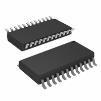
NT OR PW PACKAGE
(TOP VIEW)
T/C
A
B
D1
D2
D3
D4
D5
D6
D7
D8
GND
Rise/Fall Time
Polarity Control for Y Outputs Selects True
or Complementary Logic
Typical VOLP (Output Ground Bounce)
2.3 V at VCC = 3.3 V, TA = 25°C
Ioff Supports Partial-Power-Down Mode
Operation
Supports Mixed-Mode Voltage Operation on
All Ports
Latch-Up Performance Exceeds 250 mA Per
JESD 17
ESD Protection Exceeds JESD 22
− 2000-V Human-Body Model (A114-A)
− 200-V Machine Model (A115-A)
− 1000-V Charged-Device Model (C101)
1
24
2
23
3
22
4
21
5
20
6
19
7
18
8
17
9
16
10
15
11
14
12
13
VCC
P
N
Y1
Y2
Y3
Y4
Y5
Y6
Y7
Y8
OE
description/ordering information
The SN74LV8151 is a 10-bit universal Schmitt-trigger buffer with 3-state outputs, designed for 2-V to 5.5-V VCC
operation. The logic control (T/C) pin allows the user to configure Y1 to Y8 as noninverting or inverting outputs.
When T/C is high, the Y outputs are noninverted (true logic ), and when T/C is low, the Y outputs are inverted
(complementary logic).
When output-enable (OE) input is low, the device passes data from Dn to Yn. When OE is high, the Y outputs
are in the high-impedance state. The path A to P is a simple Schmitt-trigger buffer, and the path B to N is a simple
Schmitt-trigger inverter.
This device is fully specified for partial-power-down applications using Ioff. The Ioff circuitry disables the outputs,
preventing damaging current backflow through the device when it is powered down.
To ensure the high-impedance state during power up or power down, OE should be tied to VCC through a pullup
resistor; the minimum value of the resistor is determined by the current-sinking capability of the driver.
ORDERING INFORMATION
PDIP − NT
−40°C
85°C
−40
C to 85
C
ORDERABLE
PART NUMBER
PACKAGE†
TA
TSSOP − PW
Tube
SN74LV8151NT
Tube
SN74LV8151PW
Tape and reel
SN74LV8151PWR
TOP-SIDE
MARKING
SN74LV8151NT
LV8151
† Package drawings, standard packing quantities, thermal data, symbolization, and PCB design
guidelines are available at www.ti.com/sc/package.
Please be aware that an important notice concerning availability, standard warranty, and use in critical applications of
Texas Instruments semiconductor products and disclaimers thereto appears at the end of this data sheet.
Copyright 2004, Texas Instruments Incorporated
�������
�� ���� ���!"#$%�!� �& '("")�% $& !� *(+,�'$%�!� -$%).
�"!-('%& '!��!"# %! &*)'���'$%�!�& *)" %/) %)"#& !� �)0$&
�&%"(#)�%&
&%$�-$"- 1$""$�%2. �"!-('%�!� *"!')&&��3 -!)& �!% �)')&&$"�,2 ��',(-)
%)&%��3 !� $,, *$"$#)%)"&.
POST OFFICE BOX 655303
• DALLAS, TEXAS 75265
1
��������� �
�
��
� ��
������ ����
�����
���� ������
�
�� ������� �������
SCES610 − OCTOBER 2004
FUNCTION TABLES
INPUT
A
OUTPUT
P
L
L
H
H
INPUT
B
OUTPUT
N
L
H
H
L
INPUTS
D
OUTPUT
Y
L
L
H
L
H
L
L
H
L
L
L
H
H
H
H
X
X
Z
OE
T/C
L
L
logic diagram
A
B
T/C
D1
2
23
3
22
1
13
4
21
To Seven Other Channels
2
POST OFFICE BOX 655303
• DALLAS, TEXAS 75265
P
N
OE
Y1
��������� �
�
��
� ��
������ ����
�����
���� ������
�
�� ������� �������
SCES610 − OCTOBER 2004
absolute maximum ratings over operating free-air temperature range (unless otherwise noted)†
Supply voltage range, VCC . . . . . . . . . . . . . . . . . . . . . . . . . . . . . . . . . . . . . . . . . . . . . . . . . . . . . . . . . . −0.5 V to 7 V
Input voltage range, VI (see Note 1) . . . . . . . . . . . . . . . . . . . . . . . . . . . . . . . . . . . . . . . . . . . . . . . . . . −0.5 V to 7 V
Voltage range applied to any output in the high-impedance
or power-off state, VO (see Note 1) . . . . . . . . . . . . . . . . . . . . . . . . . . . . . . . . . . . . . . . . . . . . . . . . −0.5 V to 7 V
Output voltage range, VO (see Notes 1 and 2) . . . . . . . . . . . . . . . . . . . . . . . . . . . . . . . . . . −0.5 V to VCC + 0.5 V
Input clamp current, IIK (VI < 0) . . . . . . . . . . . . . . . . . . . . . . . . . . . . . . . . . . . . . . . . . . . . . . . . . . . . . . . . . . . −20 mA
Output clamp current, IOK (VO < 0) . . . . . . . . . . . . . . . . . . . . . . . . . . . . . . . . . . . . . . . . . . . . . . . . . . . . . . . . −50 mA
Continuous output current, IO (VO = 0 to VCC) . . . . . . . . . . . . . . . . . . . . . . . . . . . . . . . . . . . . . . . . . . . . . . ±35 mA
Continuous current through VCC or GND . . . . . . . . . . . . . . . . . . . . . . . . . . . . . . . . . . . . . . . . . . . . . . . . . . . ±70 mA
Package thermal impedance, θJA (see Note 3): NT package . . . . . . . . . . . . . . . . . . . . . . . . . . . . . . . . . 67°C/W
(see Note 4): PW package . . . . . . . . . . . . . . . . . . . . . . . . . . . . . . . . . 88°C/W
Storage temperature range, Tstg . . . . . . . . . . . . . . . . . . . . . . . . . . . . . . . . . . . . . . . . . . . . . . . . . . . −65°C to 150°C
† Stresses beyond those listed under “absolute maximum ratings” may cause permanent damage to the device. These are stress ratings only, and
functional operation of the device at these or any other conditions beyond those indicated under “recommended operating conditions” is not
implied. Exposure to absolute-maximum-rated conditions for extended periods may affect device reliability.
NOTES: 1. The input and output voltage ratings may be exceeded if the input and output current ratings are observed.
2. This value is limited to 5.5 V maximum.
3. The package thermal impedance is calculated in accordance with JESD 51-3.
4. The package thermal impedance is calculated in accordance with JESD 51-7.
POST OFFICE BOX 655303
• DALLAS, TEXAS 75265
3
��������� �
�
��
� ��
������ ����
�����
���� ������
�
�� ������� �������
SCES610 − OCTOBER 2004
recommended operating conditions (see Note 5)
VCC
VCC
MIN
MAX
2
5.5
2V
1.5
Supply voltage
3 V to 3.6 V
VCC × 0.7
VCC × 0.7
4.5 V to 5.5 V
VCC × 0.7
2.3 V to 2.7 V
VIH
High-level input voltage
2V
Low-level input voltage
VO
IOH
IOL
Input voltage
Output voltage
0
High or low state
0
3-state
0
High-level output current
Low-level output current
T/C, OE inputs
∆t/∆v
Input transition rise or fall rate
A, B, D inputs
V
VCC × 0.3
VCC × 0.3
3 V to 3.6 V
4.5 V to 5.5 V
VI
V
0.5
2.3 V to 2.7 V
VIL
UNIT
VCC × 0.3
5.5
V
V
VCC
5.5
V
2V
−50
µA
2.3 V to 2.7 V
−2
3 V to 3.6 V
−6
4.5 V to 5.5 V
−12
2V
50
2.3 V to 2.7 V
2
3 V to 3.6 V
6
4.5 V to 5.5 V
12
2.3 V to 2.7 V
200
3 V to 3.6 V
100
4.5 V to 5.5 V
20
2.3 V to 2.7 V
4
3 V to 3.6 V
3
4.5 V to 5.5 V
2
mA
µA
mA
ns/V
ms/V
TA
Operating free-air temperature
−40
85
°C
NOTES: 5. All unused inputs of the device must be held at VCC or GND to ensure proper device operation. Refer to the TI application report,
Implications of Slow or Floating CMOS Inputs, literature number SCBA004.
4
POST OFFICE BOX 655303
• DALLAS, TEXAS 75265
��������� �
�
��
� ��
������ ����
�����
���� ������
�
�� ������� �������
SCES610 − OCTOBER 2004
electrical characteristics over recommended operating free-air temperature range (unless
otherwise noted)
PARAMETER
VT+
Positive-going input
threshold voltage
VT−
Negative-going input
threshold voltage
∆VT
Hysteresis
(VT+ − VT−)
TEST CONDITIONS
A, B, and D inputs
A, B, and D inputs
A, B, and D inputs
IOL = 50 µA
IOL = 2 mA
1.75
3.3 V
2.31
II
IOZ
VI = 5.5 V or GND
VO = VCC or GND
ICC
Ioff
VI = VCC or GND, IO = 0
VI or VO = 0 to 5.5 V
Ci
VI = VCC or GND
Co
VO = VCC or GND
0.75
3.3 V
0.99
tpd
TO
(OUTPUT)
A or B
P or N
5V
1.5
0.25
1
3.3 V
0.33
1.32
5V
0.5
2
2.3 V
VCC − 0.1
2
3V
2.48
4.5 V
3.8
V
V
0.1
2.3 V
0.4
3V
0.44
4.5 V
0.55
V
0 to 5.5 V
±1
µA
5.5 V
±5
µA
5.5 V
20
µA
0
5
µA
3.3 V
3
5V
3
3.3 V
5
5V
5
free-air
LOAD
CAPACITANCE
D
T/C
V
V
2.5 V
switching characteristics over recommended operating
VCC = 2.5 V ± 0.2 V (unless otherwise noted) (see Figure 1)
FROM
(INPUT)
UNIT
3.5
2.5 V
2 V to 5.5 V
IOL = 6 mA
IOL = 12 mA
PARAMETER
MAX
2.5 V
2 V to 5.5 V
IOH = −6 mA
IOH = −12 mA
VOL
TYP
5V
IOH = −50 µA
IOH = −2 mA
VOH
MIN
VCC
Y
CL = 15 pF
pF
pF
temperature
TA = 25°C
TYP
range,
MIN
MAX
22
1
45
23
1
49
24
1
50
UNIT
ns
ten
OE
Y
12
1
25
ns
tdis
OE
Y
11
1
20
ns
A or B
P or N
26
1
52
28
1
57
29
1
58
tpd
D
T/C
Y
CL = 50 pF
ns
ten
OE
Y
15
1
30
ns
tdis
OE
Y
15
1
26
ns
POST OFFICE BOX 655303
• DALLAS, TEXAS 75265
5
��������� �
�
��
� ��
������ ����
�����
���� ������
�
�� ������� �������
SCES610 − OCTOBER 2004
switching characteristics over recommended operating
VCC = 3.3 V ± 0.3 V (unless otherwise noted) (see Figure 1)
PARAMETER
tpd
FROM
(INPUT)
TO
(OUTPUT)
A or B
P or N
free-air
LOAD
CAPACITA
NCE
range,
TA = 25°C
MIN
MAX
14
1
26
15
1
29
16
1
30
UNIT
TYP
D
Y
T/C
temperature
CL = 15 pF
ns
ten
OE
Y
9
1
16
ns
tdis
OE
Y
8
1
14
ns
A or B
P or N
17
1
32
18
1
34
tpd
D
Y
T/C
ns
20
1
36
ten
OE
Y
11
1
20
ns
tdis
OE
Y
11
1
18
ns
CL = 50 pF
switching characteristics over recommended operating
VCC = 5 V ± 0.5 V (unless otherwise noted) (see Figure 1)
PARAMETER
tpd
FROM
(INPUT)
TO
(OUTPUT)
A or B
P or N
free-air
LOAD
CAPACITA
NCE
D
Y
T/C
temperature
range,
TA = 25°C
MIN
MAX
UNIT
TYP
9
1
15
10
1
16
ns
11
1
17
ten
OE
Y
6
1
10.5
ns
tdis
OE
Y
6
1
10
ns
A or B
P or N
tpd
CL = 15 pF
D
Y
T/C
CL = 50 pF
11
1
18
12
1
20
13
1
21
ns
ten
OE
Y
8
1
12.5
ns
tdis
OE
Y
8
1
11.5
ns
noise characteristics, VCC = 3.3 V, CL = 50 pF (see Note 6)
PARAMETER
MIN
TA = 25°C
TYP
MAX
UNIT
VOL(P)
VOL(V)
Quiet output, maximum dynamic VOL
0.6
V
Quiet output, minimum dynamic VOL
−0.6
V
VOH(V)
VIH(D)
Quiet output, minimum dynamic VOH
2.9
V
High-level dynamic input voltage
2.31
VIL(D)
Low-level dynamic input voltage
NOTE 6: Characteristics are for surface-mount packages only.
6
POST OFFICE BOX 655303
V
0.99
• DALLAS, TEXAS 75265
V
��������� �
�
��
� ��
������ ����
�����
���� ������
�
�� ������� �������
SCES610 − OCTOBER 2004
operating characteristics, TA = 25°C
PARAMETER
Cpd
TEST CONDITIONS
Power dissipation capacitance
CL = No load, f = 1 MHz
POST OFFICE BOX 655303
• DALLAS, TEXAS 75265
VCC
3.3 V
5V
TYP
UNIT
15
16
pF
7
��������� �
�
��
� ��
������ ����
�����
���� ������
�
�� ������� �������
SCES610 − OCTOBER 2004
PARAMETER MEASUREMENT INFORMATION
From Output
Under Test
RL = 1 kΩ
From Output
Under Test
Test
Point
VCC
Open
S1
TEST
GND
S1
tPLH/tPHL
tPLZ/tPZL
tPHZ/tPZH
Open Drain
CL
(see Note A)
CL
(see Note A)
Open
VCC
GND
VCC
LOAD CIRCUIT FOR
3-STATE AND OPEN-DRAIN OUTPUTS
LOAD CIRCUIT FOR
TOTEM-POLE OUTPUTS
VCC
50% VCC
Timing Input
0V
tw
tsu
VCC
50% VCC
50% VCC
Input
th
VCC
50% VCC
Data Input
50% VCC
0V
0V
VOLTAGE WAVEFORMS
SETUP AND HOLD TIMES
VOLTAGE WAVEFORMS
PULSE DURATION
VCC
50% VCC
Input
50% VCC
tPLH
In-Phase
Output
50% VCC
VOH
50% VCC
VOL
VOH
50% VCC
VOL
50% VCC
0V
Output
Waveform 1
S1 at VCC
(see Note B)
tPLH
50% VCC
50% VCC
tPLZ
tPZL
tPHL
tPHL
Out-of-Phase
Output
0V
VCC
Output
Control
≈VCC
50% VCC
tPHZ
tPZH
Output
Waveform 2
S1 at GND
(see Note B)
VOLTAGE WAVEFORMS
PROPAGATION DELAY TIMES
INVERTING AND NONINVERTING OUTPUTS
VOL + 0.3 V
VOL
50% VCC
VOH − 0.3 V
VOH
≈0 V
VOLTAGE WAVEFORMS
ENABLE AND DISABLE TIMES
LOW- AND HIGH-LEVEL ENABLING
NOTES: A. CL includes probe and jig capacitance.
B. Waveform 1 is for an output with internal conditions such that the output is low, except when disabled by the output control.
Waveform 2 is for an output with internal conditions such that the output is high, except when disabled by the output control.
C. All input pulses are supplied by generators having the following characteristics: PRR ≤ 1 MHz, ZO = 50 Ω, tr ≤ 3 ns, tf ≤ 3 ns.
D. The outputs are measured one at a time, with one input transition per measurement.
E. tPLZ and tPHZ are the same as tdis.
F. tPZL and tPZH are the same as ten.
G. tPHL and tPLH are the same as tpd.
H. All parameters and waveforms are not applicable to all devices.
Figure 1. Load Circuit and Voltage Waveforms
8
POST OFFICE BOX 655303
• DALLAS, TEXAS 75265
�PACKAGE OPTION ADDENDUM
www.ti.com
14-Oct-2022
PACKAGING INFORMATION
Orderable Device
Status
(1)
Package Type Package Pins Package
Drawing
Qty
Eco Plan
(2)
Lead finish/
Ball material
MSL Peak Temp
Op Temp (°C)
Device Marking
(3)
Samples
(4/5)
(6)
SN74LV8151DGVR
ACTIVE
TVSOP
DGV
24
2000
RoHS & Green
NIPDAU
Level-1-260C-UNLIM
-40 to 85
LV8151
Samples
SN74LV8151DW
ACTIVE
SOIC
DW
24
25
RoHS & Green
NIPDAU
Level-1-260C-UNLIM
-40 to 85
LV8151
Samples
SN74LV8151DWR
ACTIVE
SOIC
DW
24
2000
RoHS & Green
NIPDAU
Level-1-260C-UNLIM
-40 to 85
LV8151
Samples
SN74LV8151PW
ACTIVE
TSSOP
PW
24
60
RoHS & Green
NIPDAU
Level-1-260C-UNLIM
-40 to 85
LV8151
Samples
SN74LV8151PWR
ACTIVE
TSSOP
PW
24
2000
RoHS & Green
NIPDAU
Level-1-260C-UNLIM
-40 to 85
LV8151
Samples
SN74LV8151PWRE4
ACTIVE
TSSOP
PW
24
2000
RoHS & Green
NIPDAU
Level-1-260C-UNLIM
-40 to 85
LV8151
Samples
(1)
The marketing status values are defined as follows:
ACTIVE: Product device recommended for new designs.
LIFEBUY: TI has announced that the device will be discontinued, and a lifetime-buy period is in effect.
NRND: Not recommended for new designs. Device is in production to support existing customers, but TI does not recommend using this part in a new design.
PREVIEW: Device has been announced but is not in production. Samples may or may not be available.
OBSOLETE: TI has discontinued the production of the device.
(2)
RoHS: TI defines "RoHS" to mean semiconductor products that are compliant with the current EU RoHS requirements for all 10 RoHS substances, including the requirement that RoHS substance
do not exceed 0.1% by weight in homogeneous materials. Where designed to be soldered at high temperatures, "RoHS" products are suitable for use in specified lead-free processes. TI may
reference these types of products as "Pb-Free".
RoHS Exempt: TI defines "RoHS Exempt" to mean products that contain lead but are compliant with EU RoHS pursuant to a specific EU RoHS exemption.
Green: TI defines "Green" to mean the content of Chlorine (Cl) and Bromine (Br) based flame retardants meet JS709B low halogen requirements of


 工商网监
湘ICP备2023018690号
工商网监
湘ICP备2023018690号
