Order
Now
Product
Folder
Support &
Community
Tools &
Software
Technical
Documents
SN74LV8154
SCLS589B – AUGUST 2004 – REVISED MAY 2020
SN74LV8154 Dual 16-Bit Binary Counters With 3-State Output Registers
Check for Samples: SN74LV8154
1 Features
3 Description
•
The SN74LV8154 device is a dual 16-bit binary
counter with 3-state output registers, designed for 2-V
to 5.5-V VCC operation.
1
•
•
•
•
•
•
•
•
Can Be Used as Two 16-Bit Counters or a Single
32-Bit Counter
8-bit counter read bus
2-V to 5.5-V VCC Operation
Maximum tpd of 25 ns at 5 V (RCLK to Y)
Typical VOLP (Output Ground Bounce)
< 0.7 V at VCC = 5 V, TA = 25°C
Typical VOHV (Output VOH Undershoot)
> 4.4 V at VCC = 5 V, TA = 25°C
Ioff Supports Partial-Power-Down Mode Operation
Latch-Up Performance Exceeds 250 mA
Per JESD 17
ESD Protection Exceeds JESD 22
– 2000-V Human Body Model (A114-A)
– 200-V Machine Model (A115-A)
– 1000-V Charged-Device Model (C101)
The counters have dedicated clock inputs. The
counters share a clocked storage register to sample
and save the counter contents. Both counters share
an asynchronous clear input. The 32-bit storage
register can be mapped on the output bus 8-bits at a
time. Four bus reads are needed to access the
contents of both stored counts. The two counters can
be chained by connecting CLKBEN to RCOA. All
clocks are positive edge triggered. All other inputs are
active low.
This device is fully specified for partial-power-down
applications using Ioff. The Ioff circuitry disables the
outputs, preventing damaging current backflow
through the device when it is powered down.
Device Information(1)
PART NUMBER
PACKAGE
BODY SIZE (NOM)
2 Applications
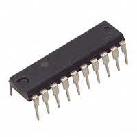
SN74LV8154N
PDIP (20)
26.92 mm x 6.35 mm
•
•
SN74LV8154PW
TSSOP (20)
6.50 mm x 4.40 mm
Up Counters
Dual Up Counters
(1) For all available packages, see the orderable addendum at
the end of the data sheet.
Simplified Schematic
R
R
R
R
R
R
CCKB
CCKBEN
R
R
R
R
R
R
R
R
R
16-Bit Counter B
R
R
R
R
R
R
R
R
R
R
R
R
R
R
R
4 to 1 Dec
Y0
4 to 1 Dec
Y1
4 to 1 Dec
Y2
4 to 1 Dec
Y3
4 to 1 Dec
Y4
4 to 1 Dec
Y5
4 to 1 Dec
Y6
4 to 1 Dec
Y7
R
R
RCLK
CCKA
CCLR
16-Bit Counter A
GAL
GAU
GBL
RCOA
GBU
1
An IMPORTANT NOTICE at the end of this data sheet addresses availability, warranty, changes, use in safety-critical applications,
intellectual property matters and other important disclaimers. PRODUCTION DATA.
�SN74LV8154
SCLS589B – AUGUST 2004 – REVISED MAY 2020
www.ti.com
Table of Contents
1
2
3
4
5
6
7
8
Features ..................................................................
Applications ...........................................................
Description .............................................................
Revision History.....................................................
Pin Configuration and Functions .........................
Specifications.........................................................
1
1
1
2
3
4
6.1
6.2
6.3
6.4
6.5
6.6
6.7
6.8
6.9
6.10
4
4
4
5
5
5
6
6
6
7
Absolute Maximum Ratings ......................................
ESD Ratings..............................................................
Recommended Operating Conditions.......................
Thermal Information ..................................................
Electrical Characteristics...........................................
Timing Requirements ................................................
Switching Characteristics - VCC = 3.3 V ± 0.3 V .......
Switching Characteristics VCC = 5 V ± 0.5 V.............
Noise Characteristics ................................................
Typical Characteristics ............................................
Parameter Measurement Information .................. 8
Detailed Description .............................................. 9
8.1
8.2
8.3
8.4
9
Overview ................................................................... 9
Functional Block Diagram ......................................... 9
Feature Description................................................... 9
Device Functional Modes........................................ 10
Application and Implementation ........................ 11
9.1 Application Information............................................ 11
9.2 Typical Application ................................................. 11
10 Power Supply Recommendations ..................... 13
11 Layout................................................................... 13
11.1 Layout Guidelines ................................................. 13
11.2 Layout Example .................................................... 13
12 Device and Documentation Support ................. 14
12.1
12.2
12.3
12.4
12.5
Documentation Support ........................................
Community Resources..........................................
Trademarks ...........................................................
Electrostatic Discharge Caution ............................
Glossary ................................................................
14
14
14
14
14
13 Mechanical, Packaging, and Orderable
Information ........................................................... 14
4 Revision History
NOTE: Page numbers for previous revisions may differ from page numbers in the current version.
Changes from Revision A (October 2015) to Revision B
Page
•
Changed body size in Device Information table ..................................................................................................................... 1
•
Changed body size in Device Information table ..................................................................................................................... 1
•
Corrected typo 'acitve-low' to active-low in the Pin Functions table. ..................................................................................... 3
Changes from Original (August 2004) to Revision A
Page
•
Added Pin Configuration and Functions section, Storage Conditions table, ESD Ratings table, Feature Description
section, Device Functional Modes, Application and Implementation section, Power Supply Recommendations
section, Layout section, Device and Documentation Support section, and Mechanical, Packaging, and Orderable
Information section ................................................................................................................................................................ 1
•
Removed Ordering Information table ..................................................................................................................................... 1
2
Submit Documentation Feedback
Copyright © 2004–2020, Texas Instruments Incorporated
Product Folder Links: SN74LV8154
�SN74LV8154
www.ti.com
SCLS589B – AUGUST 2004 – REVISED MAY 2020
5 Pin Configuration and Functions
N or PW Package
20-Pin PDIP or TSSOP
Top View
CLKA
CLKB
GAL
GAU
GBL
GBU
RCLK
RCOA
CLKBEN
GND
1
20
2
19
3
18
4
17
5
16
6
15
7
14
8
13
9
12
10
11
VCC
Y0
Y1
Y2
Y3
Y4
Y5
Y6
Y7
CCLR
Table 1. Pin Functions
PIN
I/O
DESCRIPTION
NAME
NO.
CCLR
11
I
Clock clear, asyncrounous active-low clear for both counters
CLKA
1
I
Clock A, rising edge count clock
CLKB
2
I
Clock B, rising edge count clock
CLKBEN
9
I
Clock B enable, active-low allows clocking for counter B; connect to RCOA for 32-bit counter.
GAL
3
I
Gate A lower byte, active-low puts lower byte of stored counter A on the Y bus.
GAU
4
I
Gate A upper byte, active-low puts upper byte of stored counter A on the Y bus.
GBL
5
I
Gate B lower byte, active-low puts lower byte of stored counter B on the Y bus.
GBU
6
I
Gate B upper byte, active-low puts upper byte of stored counter B on the Y bus.
GND
10
—
RCLK
7
I
Register Clock, rising edge stores counters into an internal storage register.
RCOA
8
O
Ready case overflow A, active low when counter A is full count and ready to overflow on next
clock A.
VCC
20
—
Power supply pin
Y0
19
O
Data output bit 0 (LSB)
Y1
18
O
Data output bit 1
Y2
17
O
Data output bit 2
Y3
16
O
Data output bit 3
Y4
15
O
Data output bit 4
Y5
14
O
Data output bit 5
Y6
13
O
Data output bit 6
Y7
12
O
Data output bit 7 (MSB)
Ground
Submit Documentation Feedback
Copyright © 2004–2020, Texas Instruments Incorporated
Product Folder Links: SN74LV8154
3
�SN74LV8154
SCLS589B – AUGUST 2004 – REVISED MAY 2020
www.ti.com
6 Specifications
6.1 Absolute Maximum Ratings
over operating free-air temperature range (unless otherwise noted) (1)
VCC
MIN
MAX
UNIT
Supply voltage
–0.5
7
V
(2)
VI
Input voltage
–0.5
7
V
VO
Voltage applied to any output in the high-impedance or power-off state (2)
–0.5
7
V
VO
Output voltage (2) (3)
–0.5
VCC + 0.5
V
IIK
Input clamp current
VI < 0
–20
mA
IOK
Output clamp current
VO < 0
–50
mA
IO
Continuous output current
VO = 0 to VCC
±35
mA
Continuous current through VCC or GND
±70
mA
TJ
Junction Temperature
150
°C
Tstg
Storage temperature
150
°C
(1)
(2)
(3)
–65
Stresses beyond those listed under Absolute Maximum Ratings may cause permanent damage to the device. These are stress ratings
only, which do not imply functional operation of the device at these or any other conditions beyond those indicated under Recommended
Operating Conditions. Exposure to absolute-maximum-rated conditions for extended periods may affect device reliability.
The input and output voltage ratings may be exceeded if the input and output current ratings are observed.
This value is limited to 5.5 V maximum.
6.2 ESD Ratings
VALUE
V(ESD)
(1)
(2)
Electrostatic discharge
Human body model (HBM), per ANSI/ESDA/JEDEC JS-001, all pins (1)
±2000
Charged device model (CDM), per JEDEC specification JESD22-C101, all pins (2)
±1000
UNIT
V
JEDEC document JEP155 states that 500-V HBM allows safe manufacturing with a standard ESD control process.
JEDEC document JEP157 states that 250-V CDM allows safe manufacturing with a standard ESD control process.
6.3 Recommended Operating Conditions (1)
VCC
VCC
Supply voltage
2V
VIH
High-level input voltage
MIN
MAX
2
5.5
Low-level input voltage
VI
3 V to 3.6 V
VCC × 0.7
4.5 V to 5.5 V
VCC × 0.7
VO
Output voltage
IOH
High-level output current
IOL
Low-level output current
∆t/∆v
Input transition rise and fall rate
TA
Operating free-air temperature
(1)
4
V
0.5
3 V to 3.6 V
VCC × 0.3
4.5 V to 5.5 V
VCC × 0.3
Input voltage
V
1.5
2V
VIL
UNIT
0
5.5
High or low state
0
VCC
3-state
0
5.5
2V
–50
3 V to 3.6 V
–6
4.5 V to 5.5 V
–12
2V
50
3 V to 3.6 V
6
4.5 V to 5.5 V
12
3 V to 3.6 V
100
4.5 V to 5.5 V
20
–40
V
V
V
µA
mA
µA
mA
ns/V
85
°C
All unused inputs of the device must be held at VCC or GND to ensure proper device operation. Refer to the TI application report,
Implications of Slow or Floating CMOS Inputs, SCBA004.
Submit Documentation Feedback
Copyright © 2004–2020, Texas Instruments Incorporated
Product Folder Links: SN74LV8154
�SN74LV8154
www.ti.com
SCLS589B – AUGUST 2004 – REVISED MAY 2020
6.4 Thermal Information
SN74LV8154N
SN74LV8154PW
N (PDIP)
PW (TSSOP)
20 PINS
20 PINS
THERMAL METRIC (1)
UNIT
RθJA
Junction-to-ambient thermal resistance
54.9
100.2
°C/W
RθJC(top)
Junction-to-case (top) thermal resistance
46.5
30.9
°C/W
RθJB
Junction-to-board thermal resistance
35.9
47.1
°C/W
ψJT
Junction-to-top characterization parameter
23.5
1.5
°C/W
ψJB
Junction-to-board characterization parameter
35.7
46.6
°C/W
(1)
For more information about traditional and new thermal metrics, see the Semiconductor and IC Package Thermal Metrics application
report (SPRA953).
6.5 Electrical Characteristics
over recommended operating free-air temperature range (unless otherwise noted)
PARAMETER
VOH
TEST CONDITIONS
Output high voltage
VCC
MIN
IOH = –50 µA
2V
1.9
IOH = –6 mA
3V
2.48
IOH = –12 mA
4.5 V
3.8
TYP
MAX
UNIT
V
IOL = 50 µA
2V
0.1
IOL = 6 mA
3V
0.44
4.5 V
0.55
VOL
Output low voltage
II
Input current
VI = 5.5 V or GND
0 to 5.5 V
±1
µA
IOZ
Output off current
VO = VCC or GND
5.5 V
±5
µA
ICC
Supply current
VI = VCC or GND,
5.5 V
20
µA
Ioff
Off current
VI or VO = 0 to 5.5 V
5
µA
CI
Input capacitance
VI = VCC or GND
5V
3
pF
Co
Output capacitance
VO = VCC or GND
5V
5
pF
Cpd
Power dissipation
capacitance
CL = No load,
5V
56
pF
IOL = 12 mA
IO = 0
0
CCLK = 10 MHz
RCLK = 1 MHz
V
6.6 Timing Requirements
over recommended operating free-air temperature range, VCC = 5 V ± 0.5 V (unless otherwise noted) (see Figure 3)
MIN
tw
tsu
Pulse duration
Set-up time
th
Hold time
tz (1)
Z-period
(1)
CLKA, CLKB, RCLK high or low
10
CCLR low
20
CLKBEN low before CLKB↑
10
CCLR high (inactive) before CLKA↑or CLKB↑
10
CLKA↑ or CLKB↑ before RCLK↑
10
RCLK↑ before GAL or GAU or GBL or GBU low
10
GAL or GAU or GBL or GBU high (inactive) before RCLK↑
10
CLKBEN low after CLKB↑
0
CLKA or CLKB after RCLK
0
GAL, GAU, GBL, GBU all high before one of them switches low
200
UNIT
ns
ns
ns
ns
tz condition: CL = 50 pF, RL = 1 kΩ
Submit Documentation Feedback
Copyright © 2004–2020, Texas Instruments Incorporated
Product Folder Links: SN74LV8154
5
�SN74LV8154
SCLS589B – AUGUST 2004 – REVISED MAY 2020
www.ti.com
6.7 Switching Characteristics - VCC = 3.3 V ± 0.3 V
over recommended operating free-air temperature range, VCC = 3.3 V ± 0.3 V (unless otherwise noted) (see Figure 3)
FROM
(INPUT)
PARAMETER
TO
(OUTPUT)
fMAX
tpd
tPLH
LOAD
CAPACITANCE
MIN
CL = 15 pF
40
CL = 50 pF
25
TYP
MAX
MHz
RCLK
Y
1
22
38
CLKA
RCOA
1
26
44
ns
CCLR
RCOA
1
18
32
ns
ten
GAL, GAU, GBL, GBU
Y
1
27
46
ns
tdis
GAL, GAU, GBL, GBU
Y
1
12
21
ns
RCLK
Y
1
25
42
CLKA
RCOA
1
28
46
CCLR
RCOA
1
20
35
ns
ten
GAL, GAU, GBL, GBU
Y
1
30
50
ns
tdis
GAL, GAU, GBL, GBU
Y
1
14
24
ns
tpd
tPLH
CL = 15 pF
UNIT
CL = 50 pF
ns
6.8 Switching Characteristics VCC = 5 V ± 0.5 V
over recommended operating free-air temperature range, VCC = 5 V ± 0.5 V (unless otherwise noted) (see Figure 3)
FROM
(INPUT)
PARAMETER
TO
(OUTPUT)
fMAX
tpd
tPLH
LOAD
CAPACITANCE
MIN
CL = 15 pF
40
CL = 50 pF
25
TYP
MAX
MHz
RCLK
Y
1
14
25
CLKA
RCOA
1
16
27
ns
CCLR
RCOA
1
12
20
ns
ten
GAL, GAU, GBL, GBU
Y
1
16
28
ns
tdis
GAL, GAU, GBL, GBU
Y
1
8
15
ns
RCLK
Y
1
16
27
CLKA
RCOA
1
17
28
CCLR
RCOA
1
13
21
ns
ten
GAL, GAU, GBL, GBU
Y
1
18
30
ns
tdis
GAL, GAU, GBL, GBU
Y
1
9
16
ns
MIN
TYP
MAX
tpd
tPLH
CL = 15 pF
UNIT
CL = 50 pF
ns
6.9 Noise Characteristics
VCC = 5 V, CL = 50 pF
PARAMETER
UNIT
VOL(P)
Quiet output, maximum dynamic VOL
0.7
V
VOL(V)
Quiet output, minimum dynamic VOL
–0.75
V
VOH(V)
Quiet output, minimum dynamic VOH
4.4
V
6
Submit Documentation Feedback
Copyright © 2004–2020, Texas Instruments Incorporated
Product Folder Links: SN74LV8154
�SN74LV8154
www.ti.com
SCLS589B – AUGUST 2004 – REVISED MAY 2020
CCKBEN
CCLR
CCKA
CCKB
RCLK
A
Counter
0000
0001
0002
0003
0004
B
Counter
0000
0001
0002
0003
0004
00
01
02
0100
0101
0100
0102
0103
FFFD FFFE FFFF
0000
0001
0101
0102
FFFD FFFE FFFF
0000
0001
GAL
GAU
GBL
GBU
Output Don’t Care
00
03
01
FF
RCOA
Figure 1. Timing Diagram
6.10 Typical Characteristics
12
VCC = 5-V
10
VCC = 3.3-V
ICC (mA)
8
6
4
2
0
0
5
10
15
20
25
30
35
Frequency (MHz)
40
C001
RCLK = CLKA,B / 10; No load
Figure 2. ICC vs CLKA, CLKB Frequency
Submit Documentation Feedback
Copyright © 2004–2020, Texas Instruments Incorporated
Product Folder Links: SN74LV8154
7
�SN74LV8154
SCLS589B – AUGUST 2004 – REVISED MAY 2020
www.ti.com
7 Parameter Measurement Information
From Output
Under Test
Test
Point
From Output
Under Test
RL = 1 kΩ
VCC
Open
S1
TEST
GND
CL
(see Note A)
CL
(see Note A)
S1
tPLH/tPHL
tPLZ/tPZL
tPHZ/tPZH
Open Drain
Open
VCC
GND
VCC
LOAD CIRCUIT FOR
3-STATE AND OPEN-DRAIN OUTPUTS
LOAD CIRCUIT FOR
TOTEM-POLE OUTPUTS
VCC
50% VCC
Timing Input
0V
tw
tsu
VCC
50% VCC
50% VCC
Input
th
VCC
50% VCC
Data Input
50% VCC
0V
0V
VOLTAGE WAVEFORMS
SETUP AND HOLD TIMES
VOLTAGE WAVEFORMS
PULSE DURATION
VCC
50% VCC
Input
50% VCC
tPLH
In-Phase
Output
50% VCC
VOH
50% VCC
VOL
VOH
50% VCC
VOL
tPLZ
≈VCC
50% VCC
tPZH
Output
Waveform 2
S1 at GND
(see Note B)
VOLTAGE WAVEFORMS
PROPAGATION DELAY TIMES
INVERTING AND NONINVERTING OUTPUTS
50% VCC
0V
Output
Waveform 1
S1 at VCC
(see Note B)
tPLH
50% VCC
50% VCC
tPZL
tPHL
tPHL
Out-of-Phase
Output
0V
VCC
Output
Control
VOL + 0.3 V
VOL
tPHZ
50% VCC
VOH − 0.3 V
VOH
≈0 V
VOLTAGE WAVEFORMS
ENABLE AND DISABLE TIMES
LOW- AND HIGH-LEVEL ENABLING
NOTES: A. CL includes probe and jig capacitance.
B. Waveform 1 is for an output with internal conditions such that the output is low, except when disabled by the output control.
Waveform 2 is for an output with internal conditions such that the output is high, except when disabled by the output control.
C. All input pulses are supplied by generators having the following characteristics: PRR ≤ 1 MHz, ZO = 50 Ω, tr ≤ 3 ns, tf ≤ 3 ns.
D. The outputs are measured one at a time, with one input transition per measurement.
E. t PLZ and t PHZ are the same as t dis .
F. t PZL and t PZH are the same as t en .
G. t PHL and t PLH are the same as t pd .
H. All parameters and waveforms are not applicable to all devices.
Figure 3. Load Circuit and Voltage Waveforms
8
Submit Documentation Feedback
Copyright © 2004–2020, Texas Instruments Incorporated
Product Folder Links: SN74LV8154
�SN74LV8154
www.ti.com
SCLS589B – AUGUST 2004 – REVISED MAY 2020
8 Detailed Description
8.1 Overview
The SN74LV8154 device is a dual 16-bit binary counter with 3-state output registers, designed for 2-V to 5.5-V
VCC operation. The counters have dedicated clock inputs. The counters share a storage register clock and an
asynchronous clear input. The 32-bit storage register can be mapped on the output bus 8-bit at a time. Four bus
reads are needed to access the contents of both counters. The two counters can be chained by connecting
CLKBEN to RCOA
This 16-bit counter (A or B) feeds a 16-bit storage register, and each storage register is further divided into an
upper byte and lower byte. The GAL, GAU, GBL, GBU inputs are used to select the byte that needs to be output
at Y0−Y7. CLKA is the clock for A counter, and CLKB is the clock for B counter. RCLK is the clock for the A and
B storage registers. All three clock signals are positive-edge triggered.
A 32-bit counter can be realized by connecting CLKA and CLKB together and by connecting RCOA to CLKBEN.
To ensure the high-impedance state during power up or power down, GAL, GAU, GBL, and GBU should be tied
to VCC through a pullup resistor; the minimum value of the resistor is determined by the current-sinking capability
of the driver.
This device is fully specified for partial-power-down applications using Ioff. The Ioff circuitry disables the outputs,
preventing damaging current backflow through the device when it is powered down.
8.2 Functional Block Diagram
R
R
R
R
R
R
CCKB
CCKBEN
R
R
R
R
R
R
R
R
R
16-Bit Counter B
R
R
R
R
R
R
R
R
R
R
R
R
R
R
R
4 to 1 Dec
Y0
4 to 1 Dec
Y1
4 to 1 Dec
Y2
4 to 1 Dec
Y3
4 to 1 Dec
Y4
4 to 1 Dec
Y5
4 to 1 Dec
Y6
4 to 1 Dec
Y7
R
R
RCLK
CCKA
CCLR
16-Bit Counter A
GAL
GAU
GBL
RCOA
GBU
8.3 Feature Description
Two 16-bit counters count up on each positive edge of the respective clock input. RCOA is set low when counter
A is full count. Counter B clock is gated by the CCKBEN input. Connecting RCOA to CCKBEN together chains
the counters to make one 32-bit counter.
Asynchronous CCLR input resets both counter to zero.
One 32-bit storage register records the contents of both counters on the rising edge of RCLK. The contents of
the storage register are saved until the next rising edge of the RCLK.
Mapped output bus can be set to high impedance or output 8-bits of the 32-bit storage register.
Submit Documentation Feedback
Copyright © 2004–2020, Texas Instruments Incorporated
Product Folder Links: SN74LV8154
9
�SN74LV8154
SCLS589B – AUGUST 2004 – REVISED MAY 2020
www.ti.com
8.4 Device Functional Modes
Table 2 lists the functional modes of the SN74LV8154.
Table 2. Function Table
INPUTS
10
GAL
GAU
GBL
GBU
OUTPUT
Yn
L
H
H
H
Lower byte in A storage register
H
L
H
H
Upper byte in A storage register
H
H
L
H
Lower byte in B storage register
H
H
H
L
Upper byte in B storage register
H
H
H
H
Z
Submit Documentation Feedback
Copyright © 2004–2020, Texas Instruments Incorporated
Product Folder Links: SN74LV8154
�SN74LV8154
www.ti.com
SCLS589B – AUGUST 2004 – REVISED MAY 2020
9 Application and Implementation
NOTE
Information in the following applications sections is not part of the TI component
specification, and TI does not warrant its accuracy or completeness. TI’s customers are
responsible for determining suitability of components for their purposes. Customers should
validate and test their design implementation to confirm system functionality.
9.1 Application Information
The SN74LV8154 can count any two events up to a count of 65,535 per storage register read. It can also count
one event up to a count of 4,294,967,295 per storage register read.
9.2 Typical Application
SN74LV8154
Address bus bit 0
Address bus bit 1
Address bus bit 2
Chip select Low
Chip select Low
Chip select High
A
Y0
B
Y1
C
Y2
G2A
Y3
G2B
Y4
G1
Y5
0.1 µF
Ground
Pulses to count
1
CLKA
VCC
20
More pulses to count
2
CLKB
Y0
19
Chip select AL
3
GAL
Y1
18
Chip select AU
4
GAU
Y2
17
Chip select BL
5
GBL
Y3
16
Data bus bit 3
Chip select BU
6
GBU
Y4
15
Data bus bit 4
Take a sample clock
7
RCLK
Y5
14
Data bus bit 5
8
RCOA
Y6
13
Data bus bit 6
9
CLKBEN
Y7
12
Data bus bit 7
10
GND
CCLR
11
SN74LVC138A
Ground
Data bus bit 0
Data bus bit 1
Data bus bit 2
Counter reset
Figure 4. Dual Counter With Address Mapping
9.2.1 Design Requirements
•
•
•
•
•
VCC must be acceptable for both SN74LV8154 and SN74LVC138A.
CCLR low time must be greater than 20 ns.
8 bytes of unique address space are needed.
CLKA and CLKB inputs must have input transition rate specified in Recommended Operating Conditions.
RCLK and CCLR inputs must be free of glitches to prevent accidental register saves or counter clears.
Submit Documentation Feedback
Copyright © 2004–2020, Texas Instruments Incorporated
Product Folder Links: SN74LV8154
11
�SN74LV8154
SCLS589B – AUGUST 2004 – REVISED MAY 2020
www.ti.com
Typical Application (continued)
9.2.2 Detailed Design Procedure
•
•
•
•
•
•
Connect Y0 through Y7 to the data bus.
Connect A, B, and C to lower address bus lines.
Connect G2A, G2B, and G1 to decoded addresses to provide 8 or more unique memory locations.
Connect two pulse sources to CLKA and CLKB inputs. If sources have noise or slow edges then pass the
signal through a Schmitt trigger buffer first.
If only one counter is needed, connect the single pulse source to both CLKA and CLKB.
Also connect CLKBEN to RCOA instead of ground.
Table 3. Function Table
INPUTS
(1)
(1)
OUTPUT (1)
RESULT
G1
G2A
G2B
C
B
A
Yn
L
X
X
X
X
X
Z
No action
X
H
X
X
X
X
Z
No action
X
X
H
X
X
X
Z
No action
H
L
L
L
L
L
A lower byte
Read lower byte of counter A storage register
H
L
L
L
L
H
A upper byte
Read upper byte of counter A storage register
H
L
L
L
H
L
B lower byte
Read lower byte of counter B storage register
H
L
L
L
H
H
B upper byte
Read upper byte of counter B storage register
H
L
L
H
L
L
Z
Save counters into storage register
after changing any input
H
L
L
H
L
H
Z
Reset both counters to zero
H
L
L
H
H
L
Z
No action
H
L
L
H
H
H
Z
No action
L = low, H = high, X = don't care, Z = high Impedance.
9.2.3 Application Curve
4
VIH min
3
INPUT (V)
VIL max
2
1
0
0
1
2
3
4
5
Vcc (V)
6
C001
Figure 5. Input Voltage Range vs VCC
12
Submit Documentation Feedback
Copyright © 2004–2020, Texas Instruments Incorporated
Product Folder Links: SN74LV8154
�SN74LV8154
www.ti.com
SCLS589B – AUGUST 2004 – REVISED MAY 2020
10 Power Supply Recommendations
The power supply can be any voltage between the minimum and maximum supply voltage rating located in
Recommended Operating Conditions table.
Each VCC terminal should have a good bypass capacitor to prevent power disturbance. For devices with a single
supply, a 0.1-μF capacitor is recommended. If there are multiple VCC terminals then 0.01-μF or 0.022-μF
capacitors are recommended for each power terminal. It is ok to parallel multiple bypass capacitors to reject
different frequencies of noise. Multiple bypass capacitors may be paralleled to reject different frequencies of
noise. The bypass capacitor should be installed as close to the power terminal as possible for the best results.
11 Layout
11.1 Layout Guidelines
When using multiple bit logic devices, inputs should not float. In many cases, functions or parts of functions of
digital logic devices are unused. Some examples are when only two inputs of a triple-input AND gate are used,
or when only 3 of the 4 buffer gates are used. Such input pins should not be left unconnected because the
undefined voltages at the outside connections result in undefined operational states.
Specified in Figure 6 are rules that must be observed under all circumstances. All unused inputs of digital logic
devices must be connected to a high or low bias to prevent them from floating. The logic level that should be
applied to any particular unused input depends on the function of the device. Generally they will be tied to GND
or VCC, whichever makes more sense or is more convenient.
11.2 Layout Example
VCC
Unused Input
Input
Output
Unused Input
Output
Input
Figure 6. Layout Diagram
Submit Documentation Feedback
Copyright © 2004–2020, Texas Instruments Incorporated
Product Folder Links: SN74LV8154
13
�SN74LV8154
SCLS589B – AUGUST 2004 – REVISED MAY 2020
www.ti.com
12 Device and Documentation Support
12.1 Documentation Support
12.1.1 Related Documentation
For related documentation, see the following:
Implications of Slow or Floating CMOS Inputs, SCBA004
12.2 Community Resources
TI E2E™ support forums are an engineer's go-to source for fast, verified answers and design help — straight
from the experts. Search existing answers or ask your own question to get the quick design help you need.
Linked content is provided "AS IS" by the respective contributors. They do not constitute TI specifications and do
not necessarily reflect TI's views; see TI's Terms of Use.
12.3 Trademarks
E2E is a trademark of Texas Instruments.
All other trademarks are the property of their respective owners.
12.4 Electrostatic Discharge Caution
These devices have limited built-in ESD protection. The leads should be shorted together or the device placed in conductive foam
during storage or handling to prevent electrostatic damage to the MOS gates.
12.5 Glossary
SLYZ022 — TI Glossary.
This glossary lists and explains terms, acronyms, and definitions.
13 Mechanical, Packaging, and Orderable Information
The following pages include mechanical, packaging, and orderable information. This information is the most
current data available for the designated devices. This data is subject to change without notice and revision of
this document. For browser-based versions of this data sheet, refer to the left-hand navigation.
14
Submit Documentation Feedback
Copyright © 2004–2020, Texas Instruments Incorporated
Product Folder Links: SN74LV8154
�PACKAGE OPTION ADDENDUM
www.ti.com
13-Aug-2021
PACKAGING INFORMATION
Orderable Device
Status
(1)
Package Type Package Pins Package
Drawing
Qty
Eco Plan
(2)
Lead finish/
Ball material
MSL Peak Temp
Op Temp (°C)
Device Marking
(3)
(4/5)
(6)
SN74LV8154N
ACTIVE
PDIP
N
20
20
RoHS &
Non-Green
NIPDAU
N / A for Pkg Type
-40 to 85
SN74LV8154N
SN74LV8154NE4
ACTIVE
PDIP
N
20
20
RoHS &
Non-Green
NIPDAU
N / A for Pkg Type
-40 to 85
SN74LV8154N
SN74LV8154PW
ACTIVE
TSSOP
PW
20
70
RoHS & Green
NIPDAU
Level-1-260C-UNLIM
-40 to 85
LV8154
SN74LV8154PWR
ACTIVE
TSSOP
PW
20
2000
RoHS & Green
NIPDAU
Level-1-260C-UNLIM
-40 to 85
LV8154
(1)
The marketing status values are defined as follows:
ACTIVE: Product device recommended for new designs.
LIFEBUY: TI has announced that the device will be discontinued, and a lifetime-buy period is in effect.
NRND: Not recommended for new designs. Device is in production to support existing customers, but TI does not recommend using this part in a new design.
PREVIEW: Device has been announced but is not in production. Samples may or may not be available.
OBSOLETE: TI has discontinued the production of the device.
(2)
RoHS: TI defines "RoHS" to mean semiconductor products that are compliant with the current EU RoHS requirements for all 10 RoHS substances, including the requirement that RoHS substance
do not exceed 0.1% by weight in homogeneous materials. Where designed to be soldered at high temperatures, "RoHS" products are suitable for use in specified lead-free processes. TI may
reference these types of products as "Pb-Free".
RoHS Exempt: TI defines "RoHS Exempt" to mean products that contain lead but are compliant with EU RoHS pursuant to a specific EU RoHS exemption.
Green: TI defines "Green" to mean the content of Chlorine (Cl) and Bromine (Br) based flame retardants meet JS709B low halogen requirements of


 工商网监
湘ICP备2023018690号
工商网监
湘ICP备2023018690号
