Product
Folder
Sample &
Buy
Technical
Documents
Support &
Community
Tools &
Software
SN74LVC1G57
SCES414P – NOVEMBER 2002 – REVISED NOVEMBER 2016
SN74LVC1G57 Configurable Multiple-Function Gate
1 Features
3 Description
•
•
The SN74LVC1G57 device features configurable
multiple functions. The output state is determined by
eight patterns of 3-bit input. The user can choose the
logic functions AND, OR, NAND, NOR, XNOR,
inverter, and buffer. All inputs can be connected to
VCC or GND.
1
•
•
•
•
•
•
•
Supports 5-V VCC Operation
Inputs Accept Voltages to 5.5 V
– Supports Down Translation to VCC
Max tpd of 6.3 ns at 3.3 V
Schmitt-Triggered Inputs
Low Power Consumption, 10-µA Maximum ICC
±24-mA Output Drive at 3.3 V
Ioff Supports Live Insertion, Partial-Power-Down
Mode, and Back-Drive Protection
Latch-Up Performance Exceeds 100 mA Per
JESD 78, Class II
Available in the Texas Instruments
NanoFree™ Package
2 Applications
•
•
•
•
•
•
•
•
•
•
Active Noise Cancellation (ANC)
Barcode Scanners
Blood Pressure Monitors
CPAP Machines
Cable Solutions
Embedded PCs
Field Transmitter: Temperature or Pressure
Sensors
HVAC: Heating, Ventilating, and Air Conditioning
TVs: High-Definition (HDTV), LCD, and Digital
Video Communications Systems
This device functions as an independent gate, but
because of Schmitt action, it may have different input
threshold levels for positive-going (VT+) and negativegoing (VT–) signals.
This configurable multiple-function gate is designed
for 1.65-V to 5.5-V VCC operation.
This device is fully specified for partial-power-down
applications using Ioff. The Ioff circuitry disables the
outputs, preventing damaging current backflow
through the device when it is powered down.
NanoFree™ package technology is a major
breakthrough in IC packaging concepts, using the die
as the package.
Device Information(1)
DEVICE NAME
PACKAGE
BODY SIZE (NOM)
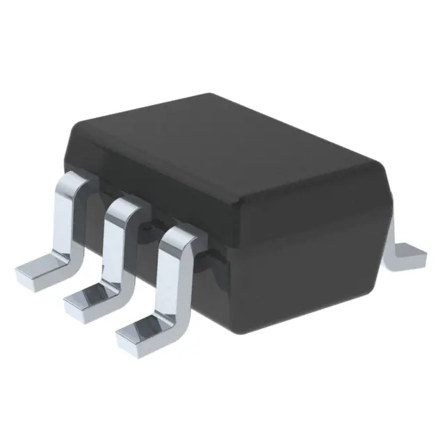
SN74LVC1G57DBV
SOT-23 (6)
2.90 mm × 1.60 mm
SN74LVC1G57DCK
SC70 (6)
2.00 mm × 1.25 mm
SN74LVC1G57DRL
SOT (6)
1.60 mm × 1.20 mm
SN74LVC1G57DRY
SON (6)
1.45 mm × 1.00 mm
SN74LVC1G57DSF
SON (6)
1.00 mm × 1.00 mm
SN74LVC1G57YZP
DSBGA (6)
1.41 mm × 0.91 mm
(1) For all available packages, see the orderable addendum at
the end of the data sheet.
Logic Diagram (Positive Logic)
Copyright © 2016, Texas Instruments Incorporated
1
An IMPORTANT NOTICE at the end of this data sheet addresses availability, warranty, changes, use in safety-critical applications,
intellectual property matters and other important disclaimers. PRODUCTION DATA.
�SN74LVC1G57
SCES414P – NOVEMBER 2002 – REVISED NOVEMBER 2016
www.ti.com
Table of Contents
1
2
3
4
5
6
7
8
Features ..................................................................
Applications ...........................................................
Description .............................................................
Revision History.....................................................
Pin Configuration and Functions .........................
Specifications.........................................................
1
1
1
2
3
4
6.1
6.2
6.3
6.4
6.5
6.6
6.7
4
4
4
5
5
6
6
Absolute Maximum Ratings ......................................
ESD Ratings..............................................................
Recommended Operating Conditions.......................
Thermal Information ..................................................
Electrical Characteristics...........................................
Switching Characteristics ..........................................
Typical Characteristics ..............................................
Parameter Measurement Information .................. 7
Detailed Description .............................................. 8
8.1 Overview ................................................................... 8
8.2 Functional Block Diagram ......................................... 8
8.3 Feature Description................................................... 8
8.4 Device Functional Modes.......................................... 8
9
Application and Implementation ........................ 10
9.1 Application Information............................................ 10
9.2 Typical Application .................................................. 10
10 Power Supply Recommendations ..................... 12
11 Layout................................................................... 12
11.1 Layout Guidelines ................................................. 12
11.2 Layout Example .................................................... 12
12 Device and Documentation Support ................. 13
12.1
12.2
12.3
12.4
12.5
12.6
Documentation Support ........................................
Receiving Notification of Documentation Updates
Community Resources..........................................
Trademarks ...........................................................
Electrostatic Discharge Caution ............................
Glossary ................................................................
13
13
13
13
13
13
13 Mechanical, Packaging, and Orderable
Information ........................................................... 13
4 Revision History
NOTE: Page numbers for previous revisions may differ from page numbers in the current version.
Changes from Revision O (December 2013) to Revision P
Page
•
Added Applications section, Device Information table, ESD Ratings table, Thermal Information table, Feature
Description section, Device Functional Modes, Application and Implementation section, Power Supply
Recommendations section, Layout section, Device and Documentation Support section, and Mechanical,
Packaging, and Orderable Information section ...................................................................................................................... 1
•
Changed Package thermal impedance, RθJA, values From: 165°C/W To: 223°C/W (DBV), From: 259°C/W To:
271.7°C/W (DCK), From: 142°C/W To: 252.5°C/W (DRL), and From: 123°C/W To: 124°C/W (YZP)................................... 5
Changes from Revision N (April 2013) to Revision O
Page
•
Changed Ioff in Features ......................................................................................................................................................... 1
•
Changed Operating temperature range.................................................................................................................................. 4
Changes from Revision M (October 2011) to Revision N
•
Page
Removed Ordering Information table; package updates now included in Package Ordering Addendum ............................. 1
Changes from Revision L (January 2007) to Revision M
Page
•
Added additional package options to the Ordering Information table .................................................................................... 1
•
Added DRY and DSF packages to data sheet....................................................................................................................... 1
2
Submit Documentation Feedback
Copyright © 2002–2016, Texas Instruments Incorporated
Product Folder Links: SN74LVC1G57
�SN74LVC1G57
www.ti.com
SCES414P – NOVEMBER 2002 – REVISED NOVEMBER 2016
5 Pin Configuration and Functions
DBV, DCK, or DRL Package
6-Pin SOT-23, SC70, or SOT
Top View
In1
1
6
In2
GND
2
5
VCC
In0
3
4
Y
DRY or DSF Package
6-Pin SON
Top View
In1
1
6
In2
GND
2
5
VCC
In0
3
4
Y
Not to scale
Not to scale
YZP Package
6-Pin DSBGA
Top View
In1
GND
In0
A1
1
6 A2
B1
2
5 B2
C1
3
4 C2
In2
VCC
Y
Pin Functions
PIN
NO.
NAME
I/O
DESCRIPTION
1
In1
I
Logic input 1
2
GND
—
3
In0
I
Logic input 0
4
Y
O
Logic output
5
VCC
—
Power
6
In2
I
Ground
Logic input 2
Submit Documentation Feedback
Copyright © 2002–2016, Texas Instruments Incorporated
Product Folder Links: SN74LVC1G57
3
�SN74LVC1G57
SCES414P – NOVEMBER 2002 – REVISED NOVEMBER 2016
www.ti.com
6 Specifications
6.1 Absolute Maximum Ratings
over operating free-air temperature range (unless otherwise noted) (1)
Supply voltage, VCC
Input voltage, VI
(2)
Voltage range (applied to any output), VO
MIN
MAX
UNIT
–0.5
6.5
V
V
–0.5
6.5
High-impedance or power-off state (2)
–0.5
6.5
High or low state (2) (3)
–0.5
VCC + 0.5
V
Input clamp current, IIK (VI < 0)
–50
mA
Output clamp current, IOK (VO < 0)
–50
mA
Continuous output current, IO
±50
mA
Continuous current through VCC or GND
±100
mA
Junction temperature, TJ
150
°C
150
°C
Storage temperature, Tstg
(1)
(2)
(3)
–65
Stresses beyond those listed under Absolute Maximum Ratings may cause permanent damage to the device. These are stress ratings
only, which do not imply functional operation of the device at these or any other conditions beyond those indicated under Recommended
Operating Conditions. Exposure to absolute-maximum-rated conditions for extended periods may affect device reliability.
The input negative-voltage and output voltage ratings may be exceeded if the input and output current ratings are observed.
The value of VCC is provided in the Recommended Operating Conditions table.
6.2 ESD Ratings
VALUE
V(ESD)
(1)
(2)
Electrostatic discharge
Human-body model (HBM), per ANSI/ESDA/JEDEC JS-001
(1)
UNIT
±2000
Charged-device model (CDM), per JEDEC specification JESD22-C101 (2)
V
±1000
JEDEC document JEP155 states that 500-V HBM allows safe manufacturing with a standard ESD control process.
JEDEC document JEP157 states that 250-V CDM allows safe manufacturing with a standard ESD control process.
6.3 Recommended Operating Conditions
over operating free-air temperature range (unless otherwise noted) (1)
Operating
MIN
MAX
1.65
5.5
UNIT
VCC
Supply voltage
VI
Input voltage
0
5.5
V
VO
Output voltage
0
VCC
V
Data retention only
1.5
VCC = 1.65 V
–4
VCC = 2.3 V
IOH
High-level output current
–8
–16
VCC = 3 V
Low-level output current
–32
VCC = 1.65 V
4
VCC = 2.3 V
8
16
VCC = 3 V
(1)
4
Operating free-air temperature
mA
24
VCC = 4.5 V
TA
mA
–24
VCC = 4.5 V
IOL
V
32
BGA package
–40
85
All other packages
–40
125
°C
All unused inputs of the device must be held at VCC or GND to ensure proper device operation, see Implications of Slow or Floating
CMOS Inputs (SCBA004).
Submit Documentation Feedback
Copyright © 2002–2016, Texas Instruments Incorporated
Product Folder Links: SN74LVC1G57
�SN74LVC1G57
www.ti.com
SCES414P – NOVEMBER 2002 – REVISED NOVEMBER 2016
6.4 Thermal Information
SN74LVC1G57
THERMAL METRIC
RθJA
(1)
Junction-to-ambient thermal resistance
RθJC(top) Junction-to-case (top) thermal resistance
DBV
(SOT)
DCK
(SOT)
DRL
(SOT)
YZP
(DSGBA)
DSF
(SON)
DRY
(SON)
6 PINS
6 PINS
6 PINS
6 PINS
6 PINS
6 PINS
UNIT
223
271.7
252.5
124
360.1
332.5
°C/W
174.4
129.8
111.6
1.4
158.8
198.5
°C/W
71
73.1
118.5
29.7
213.5
189
°C/W
RθJB
Junction-to-board thermal resistance
ψJT
Junction-to-top characterization parameter
57.1
8.3
11.8
0.5
20.4
44.3
°C/W
ψJB
Junction-to-board characterization parameter
70.3
72.4
118.8
30.1
213.2
189.7
°C/W
(1)
For more information about traditional and new thermal metrics, see the Semiconductor and IC Package Thermal Metrics application
report.
6.5 Electrical Characteristics
over recommended operating free-air temperature range (unless otherwise noted)
PARAMETER
VT+
VT–
ΔVT
TEST CONDITIONS
Positive-going input threshold voltage
Hysteresis (VT+ – VT–)
1.16
VCC = 2.3 V
1.11
1.56
1.5
1.87
VCC = 4.5 V
2.16
2.74
VCC = 5.5 V
2.61
3.33
VCC = 1.65 V
0.35
0.62
VCC = 2.3 V
0.58
0.87
VCC = 3 V
0.84
1.19
VCC = 4.5 V
1.41
1.9
VCC = 5.5 V
1.87
2.29
VCC = 1.65 V
0.3
0.62
VCC = 2.3 V
0.4
0.8
VCC = 3 V
0.53
0.87
VCC = 4.5 V
0.71
1.04
VCC = 5.5 V
0.71
1.11
1.2
VCC = 2.3 V, IOH = –8 mA
1.9
VCC = 3 V, IOH = –16 mA
2.4
VCC = 3 V, IOH = –24 mA
2.3
VCC = 4.5 V, IOH = –32 mA
3.8
V
0.1
0.3
TA = –40°C to 85°C
0.4
TA = –40°C to 125°C
0.45
VCC = 3 V, IOL = 24 mA
V
0.55
TA = –40°C to 85°C
0.55
TA = –40°C to 125°C
0.58
II
VCC = 0 V to 5.5 V, VI = 5.5 V or GND
Ioff
VCC = 0 V, VI or VO = 5.5 V
ICC
VCC = 1.65 V to 5.5 V, VI = 5.5 V or GND, IO = 0
ΔICC
VCC = 3 V to 5.5 V, one input at VCC – 0.6 V,
other inputs at VCC or GND
Ci
VCC = 3.3 V, VI = VCC or GND
(1)
V
0.45
VCC = 2.3 V, IOL = 8 mA
VCC = 4.5 V, IOL = 32 mA
V
V
VCC = 1.65 V, IOL = 4 mA
VCC = 3 V, IOL = 16 mA
UNIT
VCC – 0.1
VCC = 1.65 V, IOH = –4 mA
VCC = 1.65 V to 5.5 V, IOL = 100 µA
VOL
MAX
0.79
VCC = 1.65 V to 5.5 V, IOH = –100 µA
VOH
TYP (1)
VCC = 1.65 V
VCC = 3 V
Negative-going input threshold voltage
MIN
±1
µA
±10
µA
10
µA
500
µA
3.5
pF
All typical values are at VCC = 3.3 V, TA = 25°C
Submit Documentation Feedback
Copyright © 2002–2016, Texas Instruments Incorporated
Product Folder Links: SN74LVC1G57
5
�SN74LVC1G57
SCES414P – NOVEMBER 2002 – REVISED NOVEMBER 2016
www.ti.com
Electrical Characteristics (continued)
over recommended operating free-air temperature range (unless otherwise noted)
PARAMETER
Cpd
TEST CONDITIONS
Power dissipation capacitance
f = 10 MHz, TA = 25°C
MIN
TYP (1)
VCC = 1.8 V
20
VCC = 2.5 V
20
VCC = 3.3 V
21
VCC = 5 V
22
MAX
UNIT
pF
6.6 Switching Characteristics
over recommended operating free-air temperature range (unless otherwise noted; see Figure 3)
PARAMETER
TEST CONDITIONS
MIN
VCC = 1.8 V ± 0.15 V
TA = –40°C to 85°C
tpd
Any input to Y (output)
TA = –40°C to 125°C
TYP
MAX
3.2
14.4
VCC = 2.5 V ± 0.2 V
2
8.3
VCC = 3.3 V ± 0.3 V
1.5
6.3
VCC = 5 V ± 0.5 V
1.1
5.1
VCC = 1.8 V ± 0.15 V
3.2
16.4
VCC = 2.5 V ± 0.2 V
2
9.3
VCC = 3.3 V ± 0.3 V
1.5
7.3
VCC = 5 V ± 0.5 V
1.1
6.1
UNIT
ns
6.7 Typical Characteristics
100
3.05
3
80
2.95
60
2.9
2.85
20
VOH (V)
IOFF (nA)
40
0
-20
2.8
2.75
2.7
2.65
-40
2.6
-60
2.55
-80
2.5
-100
2.45
0
0.5
1
1.5
2
2.5
3
VIN (V)
3.5
4
4.5
5
5.5
Figure 1. Partial-Power-Down Mode IOFF Across VIN
6
0
5
D001
10
15
20
25
IOH (mA)
30
35
40
D002
Figure 2. Output Voltage (VOH) vs Current (IOH)
Submit Documentation Feedback
Copyright © 2002–2016, Texas Instruments Incorporated
Product Folder Links: SN74LVC1G57
�SN74LVC1G57
www.ti.com
SCES414P – NOVEMBER 2002 – REVISED NOVEMBER 2016
7 Parameter Measurement Information
VLOAD
S1
RL
From Output
Under Test
CL
(see Note A)
Open
GND
RL
TEST
S1
tPLH/tPHL
tPLZ/tPZL
tPHZ/tPZH
Open
VLOAD
GND
LOAD CIRCUIT
INPUTS
VCC
1.8 V ± 0.15 V
2.5 V ± 0.2 V
3.3 V ± 0.3 V
5 V ± 0.5 V
VI
tr/tf
VCC
VCC
3V
VCC
≤2 ns
≤2 ns
≤2.5 ns
≤2.5 ns
VM
VLOAD
CL
RL
V∆
VCC/2
VCC/2
1.5 V
VCC/2
2 × VCC
2 × VCC
6V
2 × VCC
30 pF
30 pF
50 pF
50 pF
1 kΩ
500 Ω
500 Ω
500 Ω
0.15 V
0.15 V
0.3 V
0.3 V
VI
Timing Input
VM
0V
tw
tsu
VI
Input
VM
VM
th
VI
Data Input
VM
VM
0V
0V
VOLTAGE WAVEFORMS
SETUP AND HOLD TIMES
VOLTAGE WAVEFORMS
PULSE DURATION
VI
VM
Input
VM
0V
VOH
VM
Output
VM
VOL
VM
0V
VLOAD/2
VM
tPZH
VOH
Output
VM
tPLZ
Output
Waveform 1
S1 at VLOAD
(see Note B)
tPLH
tPHL
VM
tPZL
tPHL
tPLH
VI
Output
Control
VM
VOL
VOL
tPHZ
Output
Waveform 2
S1 at GND
(see Note B)
VOLTAGE WAVEFORMS
PROPAGATION DELAY TIMES
INVERTING AND NONINVERTING OUTPUTS
VOL + V∆
VM
VOH − V∆
VOH
≈0 V
VOLTAGE WAVEFORMS
ENABLE AND DISABLE TIMES
LOW- AND HIGH-LEVEL ENABLING
NOTES: A. CL includes probe and jig capacitance.
B. Waveform 1 is for an output with internal conditions such that the output is low, except when disabled by the output control.
Waveform 2 is for an output with internal conditions such that the output is high, except when disabled by the output control.
C. All input pulses are supplied by generators having the following characteristics: PRR ≤ 10 MHz, ZO = 50 Ω.
D. The outputs are measured one at a time, with one transition per measurement.
E. tPLZ and tPHZ are the same as tdis.
F. tPZL and tPZH are the same as ten.
G. tPLH and tPHL are the same as tpd.
H. All parameters and waveforms are not applicable to all devices.
Figure 3. Load Circuit and Voltage Waveforms
Submit Documentation Feedback
Copyright © 2002–2016, Texas Instruments Incorporated
Product Folder Links: SN74LVC1G57
7
�SN74LVC1G57
SCES414P – NOVEMBER 2002 – REVISED NOVEMBER 2016
www.ti.com
8 Detailed Description
8.1 Overview
The SN74LVC1G57 device features configurable multiple functions. The output state is determined by eight
patterns of 3-bit input. The user can choose the logic functions AND, OR, NAND, NOR, XNOR, inverter, and
buffer. All inputs can be connected to VCC or GND.
The CMOS device has high output drive while maintaining low static power dissipation over a broad VCC
operating range.
This configurable multiple-function gate is designed for 1.65-V to 5.5-V VCC operation.
8.2 Functional Block Diagram
Copyright © 2016, Texas Instruments Incorporated
8.3 Feature Description
8.3.1 Schmitt-Trigger Inputs
Schmitt-trigger inputs are designed to provide a minimum separation between positive and negative switching
thresholds. This allows for noisy or slow inputs that would cause problems such as oscillation or excessive
current draw with normal CMOS inputs
8.3.2 Inputs Accept Voltages to 5.5 V
The SN74LVC1G57 is a configurable multiple-function gate is designed for 1.65-V to 5.5-V VCC operation. Inputs
are over-voltage tolerant up to 5.5 V. This feature allows the use of this device as a translator in a mixed 1.8-V,
3.3-V, and 5-V system environment.
8.4 Device Functional Modes
Table 1 lists the functional modes of the SN74LVC1G57 and Table 2 lists the logic configuration images.
Table 1. Function Table
INPUTS
8
OUTPUT
In2
In1
In0
Y
L
L
L
H
L
L
H
L
L
H
L
H
L
H
H
L
H
L
L
L
H
L
H
L
H
H
L
H
H
H
H
H
Submit Documentation Feedback
Copyright © 2002–2016, Texas Instruments Incorporated
Product Folder Links: SN74LVC1G57
�SN74LVC1G57
www.ti.com
SCES414P – NOVEMBER 2002 – REVISED NOVEMBER 2016
Table 2. Logic Configurations
LOGIC FUNCTION
FIGURE NO.
2-Input AND
Figure 4
2-Input AND with both inputs inverted
Figure 7
2-Input NAND with inverted input
Figure 5 and Figure 6
2-Input OR with inverted input
Figure 5 and Figure 6
2-Input NOR
Figure 7
2-Input NOR with both inputs inverted
Figure 4
2-Input XNOR
Figure 8
VCC
A
Y
B
A
VCC
A
Y
B
A
Y
B
1
6
2
5
3
4
A
B
A
Y
Y
B
Figure 4. 2-Input AND Gate
1
6
2
5
3
4
B
Y
Figure 5. 2-Input NAND Gate With Inverted A Input
VCC
VCC
A
A
Y
B
A
B
Y
Y
B
A
1
6
2
5
3
4
B
A
Y
A
B
Y
Figure 6. 2-Input NAND Gate With Inverted B Input
1
6
2
5
3
4
B
Y
Figure 7. 2-Input NOR Gate
VCC
A
Y
B
A
1
6
2
5
3
4
B
Y
Figure 8. 2-Input XNOR Gate
Submit Documentation Feedback
Copyright © 2002–2016, Texas Instruments Incorporated
Product Folder Links: SN74LVC1G57
9
�SN74LVC1G57
SCES414P – NOVEMBER 2002 – REVISED NOVEMBER 2016
www.ti.com
9 Application and Implementation
NOTE
Information in the following applications sections is not part of the TI component
specification, and TI does not warrant its accuracy or completeness. TI’s customers are
responsible for determining suitability of components for their purposes. Customers should
validate and test their design implementation to confirm system functionality.
9.1 Application Information
The SN74LVC1G57 features configurable multiple functions. The output state is determined by eight patterns of
3-bit input. The user can choose the logic functions AND, NAND, NOR, XNOR, inverter, and buffer. All inputs
can be connected to VCC or GND.
9.2 Typical Application
This application shows the SN74LVC1G57 configured as an OR gate with an inverted input. This particular
configuration is helpful for dual sensor or switch applications where one of the inputs is normally closed or a logic
high 1. Normally this application would require two external gates, but because the SN74LVC1G57 can be
configured to meet this function the application can be implemented with a single chip solution.
VCC
10 k
VCC
Sensor
SN74LVC1G57
contact
closes
circuit
1
0.1 PF
6
VCC
0.1 PF
2
5
3
4
10 k
10 k
Alarm
0.1 PF
Copyright © 2016, Texas Instruments Incorporated
Figure 9. Dual-Sensor Alarm Trigger
10
Submit Documentation Feedback
Copyright © 2002–2016, Texas Instruments Incorporated
Product Folder Links: SN74LVC1G57
�SN74LVC1G57
www.ti.com
SCES414P – NOVEMBER 2002 – REVISED NOVEMBER 2016
Typical Application (continued)
9.2.1 Design Requirements
9.2.1.1 Application Truth Table
Because we are working with two independent alarm triggers, we need to ensure that the alarm signal is only
sent whenever either condition is met. Therefore our resulting truth table will look very much like a logic OR
function. However, since we are also assuming one of the conditions to always be true, i.e. a door that should
remain closed, we make use of the inverted input in Table 3.
Table 3. Dual-Sensor Truth Table
INPUTS
OUTPUT
TRIGGER OR SWITCH
SENSOR
ALARM
H
L
X
H
L
L
X
H
H
9.2.1.2 Schmitt-Trigger Inputs
On a normal (non-Schmitt-Trigger) input the part will switch at the same point on the rising edge and falling edge.
With a slow rising edge the part will switch at the threshold. When the switch occurs it will require current from
VCC. When current is forced from VCC, the VCC level can drop causing the threshold to shift. When the threshold
shifts it will cross the input again causing the part to switch again. This can go on and on causing oscillation
which can cause excessive current. The same thing can happen if there is noise on the input. The noise can
cross the threshold multiple times and cause oscillation or multiple clocking. The solution to these problems is to
use a Schmitt-Trigger type device to translate the slow or noisy edges into something faster that will meet the
input rise and fall specs of the following device. A true Schmitt-Trigger input will not have rise and fall time
limitations.
9.2.2 Detailed Design Procedure
1. Recommended Input conditions:
– Specified high and low levels. See (VIH and VIL) in Recommended Operating Conditions.
– Inputs are overvoltage tolerant allowing them to go as high as 5.5 V at any valid VCC.
2. Recommended output conditions:
– Load currents should not exceed 20 mA on the output and 50 mA total for the part.
– Outputs should not be pulled above VCC.
9.2.3 Application Curves
6
2
5
1.5
Voltage [V]
Voltage [V]
4
3
2
1
0.5
1
0
0
VOH
VIN
VOH
VIN
-1
-0.5
0
4
8
12
Time [ns]
16
20
24
0
4
D003
Figure 10. Simulated Output VOH at 5 V and 25°C
8
12
16
Time [ns]
20
24
28
D004
Figure 11. Simulated Output VOH at 1.8 V and 25°C
Submit Documentation Feedback
Copyright © 2002–2016, Texas Instruments Incorporated
Product Folder Links: SN74LVC1G57
11
�SN74LVC1G57
SCES414P – NOVEMBER 2002 – REVISED NOVEMBER 2016
www.ti.com
10 Power Supply Recommendations
The power supply can be any voltage between the minimum and maximum supply voltage rating located in the
Recommended Operating Conditions.
Each VCC terminal should have a good bypass capacitor to prevent power disturbance. For devices with a single
supply, a 0.1-µF bypass capacitor is recommended. If there are multiple pins labeled VCC, then a 0.01-µF or
0.022-µF capacitor is recommended for each VCC because the VCC pins will be tied together internally. For
devices with dual supply pins operating at different voltages, for example VCC and VDD, a 0.1-µF bypass
capacitor is recommended for each supply pin. It is acceptable to parallel multiple bypass capacitors to reject
different frequencies of noise. 0.1-µF and 1-µF capacitors are commonly used in parallel. The bypass capacitor
should be installed as close to the power terminal as possible for best results.
11 Layout
11.1 Layout Guidelines
Reflections and matching are closely related to the loop antenna theory but are different enough to be discussed
separately from the theory. When a PCB trace turns a corner at a 90° angle, a reflection can occur. A reflection
occurs primarily because of the change of width of the trace. At the apex of the turn, the trace width increases to
1.414 times the width. This increase upsets the transmission-line characteristics, especially the distributed
capacitance and self–inductance of the trace which results in the reflection. Not all PCB traces can be straight
and therefore some traces must turn corners. Figure 12 shows progressively better techniques of rounding
corners. Only the last example (BEST) maintains constant trace width and minimizes reflections.
11.2 Layout Example
BETTER
BEST
2W
WORST
1W min.
W
Figure 12. Trace Example
12
Submit Documentation Feedback
Copyright © 2002–2016, Texas Instruments Incorporated
Product Folder Links: SN74LVC1G57
�SN74LVC1G57
www.ti.com
SCES414P – NOVEMBER 2002 – REVISED NOVEMBER 2016
12 Device and Documentation Support
12.1 Documentation Support
12.1.1 Related Documentation
For related documentation see the following:
Implications of Slow or Floating CMOS Inputs (SCBA004)
12.2 Receiving Notification of Documentation Updates
To receive notification of documentation updates, navigate to the device product folder on ti.com. In the upper
right corner, click on Alert me to register and receive a weekly digest of any product information that has
changed. For change details, review the revision history included in any revised document.
12.3 Community Resources
The following links connect to TI community resources. Linked contents are provided "AS IS" by the respective
contributors. They do not constitute TI specifications and do not necessarily reflect TI's views; see TI's Terms of
Use.
TI E2E™ Online Community TI's Engineer-to-Engineer (E2E) Community. Created to foster collaboration
among engineers. At e2e.ti.com, you can ask questions, share knowledge, explore ideas and help
solve problems with fellow engineers.
Design Support TI's Design Support Quickly find helpful E2E forums along with design support tools and
contact information for technical support.
12.4 Trademarks
NanoFree, E2E are trademarks of Texas Instruments.
All other trademarks are the property of their respective owners.
12.5 Electrostatic Discharge Caution
These devices have limited built-in ESD protection. The leads should be shorted together or the device placed in conductive foam
during storage or handling to prevent electrostatic damage to the MOS gates.
12.6 Glossary
SLYZ022 — TI Glossary.
This glossary lists and explains terms, acronyms, and definitions.
13 Mechanical, Packaging, and Orderable Information
The following pages include mechanical, packaging, and orderable information. This information is the most
current data available for the designated devices. This data is subject to change without notice and revision of
this document. For browser-based versions of this data sheet, refer to the left-hand navigation.
Submit Documentation Feedback
Copyright © 2002–2016, Texas Instruments Incorporated
Product Folder Links: SN74LVC1G57
13
�PACKAGE OPTION ADDENDUM
www.ti.com
4-Apr-2019
PACKAGING INFORMATION
Orderable Device
Status
(1)
Package Type Package Pins Package
Drawing
Qty
Eco Plan
Lead/Ball Finish
MSL Peak Temp
(2)
(6)
(3)
Op Temp (°C)
Device Marking
(4/5)
SN74LVC1G57DBVR
ACTIVE
SOT-23
DBV
6
3000
Green (RoHS
& no Sb/Br)
CU NIPDAU
Level-1-260C-UNLIM
-40 to 125
(CA7O, CA7R)
SN74LVC1G57DCKR
ACTIVE
SC70
DCK
6
3000
Green (RoHS
& no Sb/Br)
CU NIPDAU | CU SN
Level-1-260C-UNLIM
-40 to 125
(CL5, CLF, CLJ, CL
K, CLR)
SN74LVC1G57DCKRG4
ACTIVE
SC70
DCK
6
3000
Green (RoHS
& no Sb/Br)
CU NIPDAU
Level-1-260C-UNLIM
-40 to 125
CLF
SN74LVC1G57DRLR
ACTIVE
SOT-5X3
DRL
6
4000
Green (RoHS
& no Sb/Br)
CU NIPDAU |
CU NIPDAUAG
Level-1-260C-UNLIM
-40 to 125
(CL7, CLR)
SN74LVC1G57DRY2
ACTIVE
SON
DRY
6
5000
Green (RoHS
& no Sb/Br)
CU NIPDAU
Level-1-260C-UNLIM
-40 to 125
CL
SN74LVC1G57DRYR
ACTIVE
SON
DRY
6
5000
Green (RoHS
& no Sb/Br)
CU NIPDAU
Level-1-260C-UNLIM
-40 to 125
CL
SN74LVC1G57DSFR
ACTIVE
SON
DSF
6
5000
Green (RoHS
& no Sb/Br)
CU NIPDAU
Level-1-260C-UNLIM
-40 to 125
CL
SN74LVC1G57YZPR
ACTIVE
DSBGA
YZP
6
3000
Green (RoHS
& no Sb/Br)
SNAGCU
Level-1-260C-UNLIM
-40 to 85
CLN
(1)
The marketing status values are defined as follows:
ACTIVE: Product device recommended for new designs.
LIFEBUY: TI has announced that the device will be discontinued, and a lifetime-buy period is in effect.
NRND: Not recommended for new designs. Device is in production to support existing customers, but TI does not recommend using this part in a new design.
PREVIEW: Device has been announced but is not in production. Samples may or may not be available.
OBSOLETE: TI has discontinued the production of the device.
(2)
RoHS: TI defines "RoHS" to mean semiconductor products that are compliant with the current EU RoHS requirements for all 10 RoHS substances, including the requirement that RoHS substance
do not exceed 0.1% by weight in homogeneous materials. Where designed to be soldered at high temperatures, "RoHS" products are suitable for use in specified lead-free processes. TI may
reference these types of products as "Pb-Free".
RoHS Exempt: TI defines "RoHS Exempt" to mean products that contain lead but are compliant with EU RoHS pursuant to a specific EU RoHS exemption.
Green: TI defines "Green" to mean the content of Chlorine (Cl) and Bromine (Br) based flame retardants meet JS709B low halogen requirements of


 工商网监
湘ICP备2023018690号
工商网监
湘ICP备2023018690号

