Product
Folder
Order
Now
Support &
Community
Tools &
Software
Technical
Documents
SN54LVCH245A, SN74LVCH245A
SCES008Q – JULY 1995 – REVISED SEPTEMBER 2018
SNx4LVCH245A Octal Bus Transceivers With Tri-State Outputs
1 Features
2 Applications
•
•
•
•
•
•
•
•
•
•
1
•
•
•
•
•
•
•
Operate From 1.65 V to 3.6 V
Inputs Accept Voltages to 5.5 V
Max tpd of 6.3 ns at 3.3 V
Typical VOLP (Output Ground Bounce)
2 V at VCC = 3.3 V, TA = 25°C
Support Mixed-Mode Signal Operation on All
Ports (5-V Input/Output Voltage With
3.3-V VCC)
Ioff Supports Live Insertion, Partial-Power-Down
Mode, and Back-Drive Protection
Bus Hold on Data Inputs Eliminates the Need for
External Pullup or Pulldown Resistors
Latch-Up Performance Exceeds 250 mA Per
JESD 17
ESD Protection Exceeds JESD 22
– 2000-V Human-Body Model (A114-A)
– 200-V Machine Model (A115-A)
On Products Compliant to MIL-PRF-38535,
All Parameters Are Tested Unless Otherwise
Noted. On All Other Products, Production
Processing Does Not Necessarily Include Testing
of All Parameters.
Servers
PCs and Notebooks
Network Switches
Wearable Health and Wellness Devices
Telecom Infrastructures
Electronic Points of Sale
3 Description
The SN54LVCH245A octal bus transceiver is
designed for 2.7-V to 3.6-V VCC operation, and the
SN74LVCH245A octal bus transceiver is designed for
1.65-V to 3.6-V VCC operation. Inputs can be driven
from either 3.3-V or 5-V devices. This feature allows
the use of these devices as translators in a mixed
3.3-V/5-V system environment.
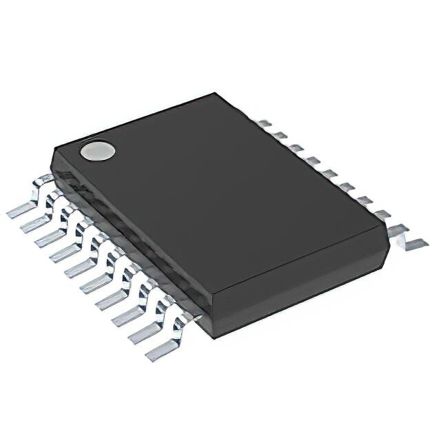
Device Information(1)
PART NUMBER
PACKAGE
BODY SIZE (NOM)
SN74LVCH245ADBR
SSOP (20)
7.20 mm × 5.30 mm
SN74LVCH245ADGVR
TVSOP (20)
5.00 mm × 4.40 mm
SN74LVCH245ADWR
SOIC (20)
12.80 mm × 7.50 mm
SN74LVCH245ANSR
SO (20)
12.60 mm × 5.30 mm
SN74LVCH245APWR
TSSOP (20)
6.50 mm × 4.40 mm
SN74LVCH245ARGYR
VQFN (20)
4.50 mm × 3.50 mm
SN74LVCH245AZQNR
BGA
MICROSTAR
JUNIOR (20)
4.00 mm × 3.00 mm
SN74LVCH245AZXYR
BGA
MICROSTAR
JUNIOR (20)
3.00 mm × 2.50 mm
(1) For all available packages, see the orderable addendum at
the end of the data sheet.
Simplified Schematic
DIR
OE
B
An
Bn
A
1
An IMPORTANT NOTICE at the end of this data sheet addresses availability, warranty, changes, use in safety-critical applications,
intellectual property matters and other important disclaimers. PRODUCTION DATA.
�SN54LVCH245A, SN74LVCH245A
SCES008Q – JULY 1995 – REVISED SEPTEMBER 2018
www.ti.com
Table of Contents
1
2
3
4
5
6
Features ..................................................................
Applications ...........................................................
Description .............................................................
Revision History.....................................................
Pin Configuration and Functions .........................
Specifications.........................................................
1
1
1
2
4
7
6.1 Absolute Maximum Ratings ..................................... 7
6.2 ESD Ratings.............................................................. 7
6.3 Recommended Operating Conditions:
SN74LVCH245A ....................................................... 8
6.4 Recommended Operating Conditions:
SN54LVCH245A ....................................................... 9
6.5 Thermal Information .................................................. 9
6.6 Electrical Characteristics: SN74LVCH245A............ 10
6.7 Electrical Characteristics: SN54LVCH245A............ 11
6.8 Switching Characteristics: SN74LVCH245A, –40°C
TO 85°C ................................................................... 12
6.9 Switching Characteristics: SN74LVCH245A, –40°C
TO 125°C ................................................................. 12
6.10 Switching Characteristics: SN54LVCH245A......... 13
6.11 Operating Characteristics...................................... 13
6.12 Typical Characteristics .......................................... 13
7
8
Parameter Measurement Information ................ 14
Detailed Description ............................................ 16
8.1
8.2
8.3
8.4
9
Overview .................................................................
Functional Block Diagram .......................................
Feature Description.................................................
Device Functional Modes........................................
16
16
16
18
Application and Implementation ........................ 19
9.1 Application Information............................................ 19
9.2 Typical Application ................................................. 19
10 Power Supply Recommendations ..................... 20
11 Layout................................................................... 21
11.1 Layout Guidelines ................................................. 21
11.2 Layout Example .................................................... 21
12 Device and Documentation Support ................. 22
12.1
12.2
12.3
12.4
Related Links ........................................................
Trademarks ...........................................................
Electrostatic Discharge Caution ............................
Glossary ................................................................
22
22
22
22
13 Mechanical, Packaging, and Orderable
Information ........................................................... 22
4 Revision History
Changes from Revision P (July 2014) to Revision Q
Page
•
Changed part number column to include specific orderable parts. ....................................................................................... 1
•
Removed package name GQN. ............................................................................................................................................ 6
•
Added ZXY package pinout section. ..................................................................................................................................... 6
•
Changed Handling Ratings to ESD ratings. .......................................................................................................................... 7
•
Deleted storage temperature from ESD Ratings table. .......................................................................................................... 7
•
Changed only include commercial device specifications in this table. ................................................................................. 10
•
Added new table for military device specifications. ............................................................................................................. 11
•
Deleted bulleted list of features. .......................................................................................................................................... 16
•
Added Output Types, Input Types, Clamp Diode Structure, and Special Features sections. ............................................. 16
Changes from Revision O (December 2005) to Revision P
Page
•
Updated document to new TI data sheet standards. ............................................................................................................. 1
•
Deleted Ordering Information table. ....................................................................................................................................... 1
•
Updated Ioff Feature bullet. ..................................................................................................................................................... 1
•
Added Military Disclaimer to Features list. ............................................................................................................................. 1
•
Added Applications. ................................................................................................................................................................ 1
•
Added Device Information table. ............................................................................................................................................ 1
•
Added Handling Ratings table. ............................................................................................................................................... 7
•
Changed MAX operating temperature to 125°C. ................................................................................................................... 8
•
Added Thermal Information table. .......................................................................................................................................... 9
•
Added –40°C TO 125°C to Electrical Characteristics table.................................................................................................. 10
•
Added data to –40°C TO 85°C Switching Characteristics table........................................................................................... 12
•
Added Switching Characteristics table for –40°C to 125°C for SN74LVCH245A. ............................................................... 12
2
Submit Documentation Feedback
Copyright © 1995–2018, Texas Instruments Incorporated
Product Folder Links: SN54LVCH245A SN74LVCH245A
�SN54LVCH245A, SN74LVCH245A
www.ti.com
SCES008Q – JULY 1995 – REVISED SEPTEMBER 2018
•
Added data to Operating Characteristics table. ................................................................................................................... 13
•
Added Typical Characteristics. ............................................................................................................................................. 13
•
Added Detailed Description section...................................................................................................................................... 16
•
Added Application and Implementation section.................................................................................................................... 19
Copyright © 1995–2018, Texas Instruments Incorporated
Product Folder Links: SN54LVCH245A SN74LVCH245A
Submit Documentation Feedback
3
�SN54LVCH245A, SN74LVCH245A
SCES008Q – JULY 1995 – REVISED SEPTEMBER 2018
www.ti.com
5 Pin Configuration and Functions
SN54LVCH245A
20-Pin J or W Package
Top View
19
3
18
4
17
5
16
6
15
7
14
8
13
9
12
10
11
5
17
6
16
7
15
8
14
9 10 11 12 13
A8
GND
B8
B7
B6
A3
A4
A5
A6
A7
3 2 1 20 19
18
4
4
Submit Documentation Feedback
B1
B2
B3
B4
B5
20
19
18
17
16
15
14
13
12
11
VCC
OE
B1
B2
B3
B4
B5
B6
B7
B8
SN74LVCH245A
20-Pin Count RGY Package
Top View
OE
A2
A1
DIR
VCC
SN54LVCH245A
20-Pin Count FK Package
Top View
1
2
3
4
5
6
7
8
9
10
A1
A2
A3
A4
A5
A6
A7
A8
VCC
2
DIR
A1
A2
A3
A4
A5
A6
A7
A8
GND
VCC
OE
B1
B2
B3
B4
B5
B6
B7
B8
1
20
2
19 OE
3
18 B1
17 B2
4
16 B3
15 B4
5
6
14 B5
13 B6
7
8
12 B7
9
10
11
B8
20
DIR
1
GND
DIR
A1
A2
A3
A4
A5
A6
A7
A8
GND
SN74LVCH245A
20-Pin Count DB, DGV. DW, NS or PW Package
Top View
Copyright © 1995–2018, Texas Instruments Incorporated
Product Folder Links: SN54LVCH245A SN74LVCH245A
�SN54LVCH245A, SN74LVCH245A
www.ti.com
SCES008Q – JULY 1995 – REVISED SEPTEMBER 2018
Pin Functions
PIN
NO.
NAME
I/O
DESCRIPTION
Direction select
1
DIR
I
2
A1
I/O
A1 input or output
3
A2
I/O
A2 input or output
4
A3
I/O
A3 input or output
5
A4
I/O
A4 input or output
6
A5
I/O
A5 input or output
7
A6
I/O
A6 input or output
8
A7
I/O
A7 input or output
9
A8
I/O
A8 input or output
10
GND
—
Ground
11
Y8
I/O
Y8 input or output
12
Y7
I/O
Y7 input or output
13
Y6
I/O
Y6 input or output
14
Y5
I/O
Y5 input or output
15
Y4
I/O
Y4 input or output
16
Y3
I/O
Y3 input or output
17
Y2
I/O
Y2 input or output
18
Y1
I/O
Y1 input or output
19
OE
I
20
VCC
—
Output enable, active low
Positive Supply
Copyright © 1995–2018, Texas Instruments Incorporated
Product Folder Links: SN54LVCH245A SN74LVCH245A
Submit Documentation Feedback
5
�SN54LVCH245A, SN74LVCH245A
SCES008Q – JULY 1995 – REVISED SEPTEMBER 2018
www.ti.com
ZQN PACKAGE
(TOP VIEW)
1
2
3
4
A
B
C
D
E
Pin Assignments: ZQN Package
1
2
3
4
A
A1
DIR
VCC
OE
B
A3
B2
A2
B1
C
A5
A4
B4
B3
D
A7
B6
A6
B5
E
GND
A8
B8
B7
ZXY PACKAGE
(TOP VIEW)
1
2
3
4
5
A
B
C
D
Pin Assignments: ZXY Package
6
1
2
3
4
A
A7
A6
A4
A2
DIR
B
A8
A5
A3
A1
VCC
C
GND
B6
B4
B2
OE
D
B8
B7
B5
B3
B1
Submit Documentation Feedback
5
Copyright © 1995–2018, Texas Instruments Incorporated
Product Folder Links: SN54LVCH245A SN74LVCH245A
�SN54LVCH245A, SN74LVCH245A
www.ti.com
SCES008Q – JULY 1995 – REVISED SEPTEMBER 2018
6 Specifications
6.1 Absolute Maximum Ratings
over operating free-air temperature range (unless otherwise noted) (1)
MIN
Supply voltage range, VCC
Input voltage range, VI
(2)
MAX
UNIT
–0.5
6.5
V
–0.5
6.5
V
Voltage range applied to any output in the high-impedance or power-off state, VO (2)
–0.5
6.5
V
Voltage range applied to any output in the high or low state, VO (2) (3)
–0.5
VCC + 0.5
V
Input clamp current, IIK
VI < 0
–50
mA
Output clamp current, IOK
VO < 0
–50
mA
±50
mA
Continuous current through VCC or GND
±100
mA
Operating virtual junction temperature, Tj
150
°C
150
°C
Continuous output current, IO
Storage temperature range, Tstg
(1)
(2)
(3)
–65
Stresses beyond those listed under Absolute Maximum Ratings may cause permanent damage to the device. These are stress ratings
only, and functional operation of the device at these or any other conditions beyond those indicated under Recommended Operating
Conditions is not implied. Exposure to absolute-maximum-rated conditions for extended periods may affect device reliability.
The input and output negative-voltage ratings may be exceeded if the input and output current ratings are observed.
The value of VCC is provided in the Recommended Operating Conditions table.
6.2 ESD Ratings
MIN
V(ESD)
(1)
(2)
Electrostatic discharge
MAX
Human body model (HBM), per ANSI/ESDA/JEDEC JS-001, all
pins (1)
0
2000
Charged device model (CDM), per JEDEC specification
JESD22-C101, all pins (2)
0
1500
UNIT
V
JEDEC document JEP155 states that 500-V HBM allows safe manufacturing with a standard ESD control process.
JEDEC document JEP157 states that 250-V CDM allows safe manufacturing with a standard ESD control process.
Copyright © 1995–2018, Texas Instruments Incorporated
Product Folder Links: SN54LVCH245A SN74LVCH245A
Submit Documentation Feedback
7
�SN54LVCH245A, SN74LVCH245A
SCES008Q – JULY 1995 – REVISED SEPTEMBER 2018
www.ti.com
6.3 Recommended Operating Conditions: SN74LVCH245A
over operating free-air temperature range (unless otherwise noted) (1)
MIN
VCC
Supply voltage
VIH
High-level input voltage
Operating
MAX
1.65
Data retention only
VI
Input voltage
1.7
VCC = 2.7 V to 3.6 V
2
Output voltage
0.7
High-level output current
IOL
Low-level output current
Δt/Δv
Input transition rise or fall rate
TA
Operating free-air temperature
(1)
8
V
0.8
0
5.5
High or low state
0
VCC
Tri-state
0
5.5
VCC = 1.65 V
IOH
V
0.35 × VCC
VCC = 2.3 V to 2.7 V
VCC = 2.7 V to 3.6 V
VO
V
0.65 × VCC
VCC = 2.3 V to 2.7 V
VCC = 1.65 V to 1.95 V
Low-level input voltage
3.6
1.5
VCC = 1.65 V to 1.95 V
VIL
UNIT
V
V
–4
VCC = 2.3 V
–8
VCC = 2.7 V
–12
VCC = 3 V
–24
VCC = 1.65 V
4
VCC = 2.3 V
8
VCC = 2.7 V
12
VCC = 3 V
24
–40
mA
mA
10
ns/V
125
°C
All unused control inputs of the device must be held at VCC or GND to ensure proper device operation. For more information, see the
Implications of Slow or Floating CMOS Inputs application report.
Submit Documentation Feedback
Copyright © 1995–2018, Texas Instruments Incorporated
Product Folder Links: SN54LVCH245A SN74LVCH245A
�SN54LVCH245A, SN74LVCH245A
www.ti.com
SCES008Q – JULY 1995 – REVISED SEPTEMBER 2018
6.4 Recommended Operating Conditions: SN54LVCH245A
over operating free-air temperature range (unless otherwise noted) (1)
MIN
VCC
Supply voltage
VIH
High-level input voltage
Operating
MAX
2
Data retention only
UNIT
3.6
1.5
V
VCC = 1.65 V to 1.95 V
VCC = 2.3 V to 2.7 V
V
VCC = 2.7 V to 3.6 V
2
VCC = 1.65 V to 1.95 V
VIL
Low-level input voltage
VI
Input voltage
VCC = 2.3 V to 2.7 V
V
VCC = 2.7 V to 3.6 V
VO
Output voltage
0.8
0
5.5
High or low state
0
VCC
Tri-state
0
5.5
V
V
VCC = 1.65 V
IOH
VCC = 2.3 V
High-level output current
VCC = 2.7 V
–12
VCC = 3 V
–24
mA
VCC = 1.65 V
IOL
Low-level output current
Δt/Δv
Input transition rise or fall rate
TA
Operating free-air temperature
(1)
VCC = 2.3 V
VCC = 2.7 V
12
VCC = 3 V
24
–55
mA
10
ns/V
125
°C
All unused control inputs of the device must be held at VCC or GND to ensure proper device operation. For more information, see the
Implications of Slow or Floating CMOS Inputs application report.
6.5 Thermal Information
SN74LVCH245A
THERMAL METRIC (1)
DB
DGV
DW
NS
PW
RGY
ZQN
ZXY
UNIT
20 PINS
RθJA
Junction-to-ambient thermal
resistance
94.5
114.7
88.3
74.7
102.5
41.4
129.3
123.5
RθJC(top)
Junction-to-case (top) thermal
resistance
56.2
29.8
51.1
40.5
35.9
47.7
75.3
58.9
RθJB
Junction-to-board thermal
resistance
49.7
56.2
50.9
42.3
53.5
17.1
77.6
74.8
ψJT
Junction-to-top characterization
parameter
18.1
0.8
20.0
14.3
2.2
1.4
2.6
2.0
ψJB
Junction-to-board characterization
parameter
49.2
55.5
50.5
41.9
52.9
17.1
73.2
74.4
RθJC(bot)
Junction-to-case (bottom) thermal
resistance
n/a
n/a
n/a
n/a
n/a
9.8
n/a
n/a
(1)
°C/W
For more information about traditional and new thermal metrics, see the IC Package Thermal Metrics application report.
Copyright © 1995–2018, Texas Instruments Incorporated
Product Folder Links: SN54LVCH245A SN74LVCH245A
Submit Documentation Feedback
9
�SN54LVCH245A, SN74LVCH245A
SCES008Q – JULY 1995 – REVISED SEPTEMBER 2018
www.ti.com
6.6 Electrical Characteristics: SN74LVCH245A
over recommended operating free-air temperature range (unless otherwise noted)
PARAMETER
TEST CONDITIONS
VCC
IOH = –100 µA
High-level
output voltage
VOH
1.65 V to 3.6 V
Low-level
output voltage
1.2
1.7
1.7
2.7 V
2.2
2.2
2.4
TYP (1)
MAX
UNIT
V
3V
2.4
IOH = –24 mA
3V
2.2
IOL = 100 µA
1.65 V to 3.6 V
0.2
0.20
IOL = 4 mA
1.65 V
0.45
0.45
IOL = 8 mA
2.3 V
0.7
0.7
IOL = 12 mA
2.7 V
0.4
0.4
IOL = 24 mA
3V
0.55
0.55
3.6 V
±5
±5
µA
0V
±10
±20
µA
Input and output
power-off
leakage current
VI or VO = 5.5 V
VI = 0.58 V
1.65 V
VI = 1.07 V
VI = 0.7 V
2.3 V
VI = 1.7 V
VI = 0.8 V
3V
VI = 2 V
VI = 0 to 3.6 V (2)
IOZ
VCC
– 0.2
1.2
Ioff
High-impedance
state output current
VCC
– 0.2
2.3 V
Control inputs:
VI = 0 to 5.5 V
(3)
MIN
1.65 V
Input current
Input hold current
–40°C TO 125°C
MAX
IOH = –8 mA
II
II(hold)
TYP (1)
IOH = –4 mA
IOH = –12 mA
VOL
–40°C TO 85°C
MIN
2.2
25
25
–25
–25
45
45
–45
–45
75
75
–75
µA
–75
3.6 V
VO = 0 V or (VCC to 5.5 V)
V
±500
±500
2.3 V to 3.6 V
±5
±15
VI = VCC or GND
IO = 0
3.6 V
10
10
3.6 V ≤ VI ≤ 5.5 V (4)
IO = 0
3.6 V
10
10
2.7 V to 3.6 V
500
500
µA
ICC
Supply current
ΔICC
Supply-current
change
One input at VCC – 0.6 V, other inputs at VCC or
GND
Ci
Input capacitance
Control inputs:
VI = VCC or GND
3.3 V
4
pF
Cio
Input and output
capacitance
A or B port:
VO = VCC or GND
3.3 V
5.50
pF
(1)
(2)
(3)
(4)
10
µA
µA
All typical values are VCC = 3.3 V, TA = 25°C.
The bus-hold maximum dynamic current requirement to switch the input from one state to another state.
For the total leakage current in an I/O port, see the II(hold) specification for the input voltage condition 0 V < VI < VCC, and the IOZ
specification for the input voltage conditions VI = 0 V or VI = VCC to 5.5 V. A bus-hold current with an input voltage greater than VCC is
negligible.
This only applies when in a disabled state.
Submit Documentation Feedback
Copyright © 1995–2018, Texas Instruments Incorporated
Product Folder Links: SN54LVCH245A SN74LVCH245A
�SN54LVCH245A, SN74LVCH245A
www.ti.com
SCES008Q – JULY 1995 – REVISED SEPTEMBER 2018
6.7 Electrical Characteristics: SN54LVCH245A
over recommended operating free-air temperature range (unless otherwise noted)
PARAMETER
TEST CONDITIONS
VCC
IOH = –100 µA
High-level
output voltage
VOH
Low-level
output voltage
VOL
II
Input current
II(hold)
Input hold current
2.7 V to 3.6 V
IOZ
2.2
2.4
IOH = –24 mA
3V
2.2
IOL = 100 µA
2.7 V to 3.6 V
IOL = 12 mA
2.7 V
0.4
IOL = 24 mA
3V
0.55
Control inputs:
VI = 0 to 5.5 V
3V
VI = 2 V
(2)
VO = 0 V or (VCC to 5.5 V)
0.2
±5
V
µA
75
–75
µA
3.6 V
±500
2.3 V to 3.6 V
±15
µA
VI = VCC or GND
IO = 0
3.6 V
10
3.6 V ≤ VI ≤ 5.5 V (4)
IO = 0
3.6 V
10
2.7 V to 3.6 V
500
µA
4
12
pF
5.5
12
pF
Supply current
ΔICC
Supply-current change
One input at VCC – 0.6 V, other inputs at VCC or
GND
Ci
Input capacitance
Control inputs:
VI = VCC or GND
3.3 V
Cio
Input and output
capacitance
A or B port:
VO = VCC or GND
3.3 V
(4)
UNIT
V
3.6 V
ICC
(1)
(2)
(3)
MAX
VCC – 0.2
3V
VI = 0 to 3.6 V
High-impedance state
output current
TYP (1)
2.7 V
IOH = –12 mA
VI = 0.8 V
(3)
MIN
µA
All typical values are VCC = 3.3 V, TA = 25°C.
The bus-hold maximum dynamic current requirement to switch the input from one state to another state.
For the total leakage current in an I/O port, see the II(hold) specification for the input voltage condition 0 V < VI < VCC, and the IOZ
specification for the input voltage conditions VI = 0 V or VI = VCC to 5.5 V. A bus-hold current with an input voltage greater than VCC is
negligible.
This only applies when in a disabled state.
Copyright © 1995–2018, Texas Instruments Incorporated
Product Folder Links: SN54LVCH245A SN74LVCH245A
Submit Documentation Feedback
11
�SN54LVCH245A, SN74LVCH245A
SCES008Q – JULY 1995 – REVISED SEPTEMBER 2018
www.ti.com
6.8 Switching Characteristics: SN74LVCH245A, –40°C TO 85°C
over recommended operating free-air temperature range (unless otherwise noted) (see Parameter Measurement Information)
PARAMETER
TEST
CONDITIONS
VCC = 1.8 V
± 0.15 V
MIN
VCC = 2.5 V
± 0.2 V
VCC = 2.7 V
VCC = 3.3 V
± 0.3 V
UNIT
MAX
MIN MAX
MIN MAX
MIN
MAX
tpd
Propagation
delay time
Input A or B to B or A output
12.7
8.3
7.3
1.5
6.3
ns
ten
Enable time
Input OE to A or B output
15.3
10.5
9.5
1.5
8.5
ns
tdis
Disable time
Input OE to A or B output
17
9.5
8.5
1.5
7.5
ns
tsk(o)
Output skew
1
1
1
1
ns
6.9 Switching Characteristics: SN74LVCH245A, –40°C TO 125°C
over recommended operating free-air temperature range (unless otherwise noted) (see Parameter Measurement Information)
PARAMETER
TEST
CONDITIONS
VCC = 1.8 V
± 0.15 V
MIN
VCC = 2.5 V
± 0.2 V
VCC = 2.7 V
VCC = 3.3 V
± 0.3 V
UNIT
MAX
MIN MAX
MIN MAX
MIN MAX
9.1
7.8
1.5
6.7
ns
tpd
Propagation
delay time
Input A or B to B or A output
13.7
ten
Enable time
Input OE to A or B output
16.8
12
10
1.5
9.1
ns
tdis
Disable time
Input OE to A or B output
18
10.5
8.7
1.5
7.8
ns
tPLH
Propagation
delay time
(low-level to
high-level output)
Input A to Y output
CL = 50 pF
8.5
1
9.5
tPHL
Propagation
delay time
(high-level to
low-level output)
Input A to Y output
CL = 50 pF
5.4
7.5
1
8.5
1
8.5
1
9.5
tPZH
Enable time
(to high level)
Input OE to Y output
CL = 50 pF
6.2
9.3
1
10.5
1
10.5
1
11.5
tPZL
Enable time
(to low level)
Input OE to Y output
CL = 50 pF
6.2
9.3
1
10.5
1
10.5
1
11.5
tPHZ
Disable time
(to high level)
Input OE to Y output
CL = 50 pF
6.7
9.2
1
10.5
1
10.5
1
11
tPLZ
Disable time
(to low level)
Input OE to Y output
CL = 50 pF
6.7
9.2
1
10.5
1
10.5
1
11
tsk(o)
Output skew
CL = 50 pF
(1)
12
5.4
7.5
1
8.5
1
ns
ns
ns
1 (1)
1
1
1
ns
With products compliant to MIL-PRF-38535, this parameter does not apply.
Submit Documentation Feedback
Copyright © 1995–2018, Texas Instruments Incorporated
Product Folder Links: SN54LVCH245A SN74LVCH245A
�SN54LVCH245A, SN74LVCH245A
www.ti.com
SCES008Q – JULY 1995 – REVISED SEPTEMBER 2018
6.10 Switching Characteristics: SN54LVCH245A
over recommended operating free-air temperature range (unless otherwise noted) (see Parameter Measurement Information)
VCC = 3.3 V
± 0.3 V
VCC = 2.7 V
TEST
CONDITIONS
PARAMETER
MIN
MAX
MIN
UNIT
MAX
tpd
Propagation delay time
Input A or B to B or A output
8
1
7
ns
ten
Enable time
Input OE to A or B output
9.5
1
8.5
ns
tdis
Disable time
Input OE to A or B output
8.5
1
7.5
ns
6.11 Operating Characteristics
TA = 25°C
Power dissipation capacitance
per transceiver
Cpd
VCC = 1.8 V
VCC = 2.5 V
VCC = 3.3 V
TYP
TYP
TYP
Outputs enabled
42
43
47
Outputs disabled
1
1
2
TEST
CONDITIONS
PARAMETER
f = 10 MHz
UNIT
pF
6.12 Typical Characteristics
6
4
TPD in ns
3.5
5
3
TPD (ns)
TPD (ns)
4
3
2.5
2
1.5
2
1
1
0.5
TPD in ns
0
0
0.5
1
1.5
2
VCC (V)
2.5
3
3.5
0
-100
-50
D001
Figure 1. SN74LVCH245A TPD Across VCC at 25°C
0
50
Temperature (qC)
100
150
D002
Figure 2. SN74LVCH245A TPD Across Temperature at 3.3 V
Copyright © 1995–2018, Texas Instruments Incorporated
Product Folder Links: SN54LVCH245A SN74LVCH245A
Submit Documentation Feedback
13
�SN54LVCH245A, SN74LVCH245A
SCES008Q – JULY 1995 – REVISED SEPTEMBER 2018
www.ti.com
7 Parameter Measurement Information
(1)
CL includes probe and jig capacitance.
VLOAD
From Output
Under Test
RL
CL(1)
Open
S1
RL
Figure 3. Load Circuit
Table 1. Test Load Switch Position
TEST
S1
tPLH / tPHL
Open
tPLZ / tPZL
VLOAD
tPHZ / tPZH
GND
Table 2. Test and Measurement Conditions
INPUTS
VCC
VM
VLOAD
CL
≤ 2 ns
VCC / 2
2 × VCC
≤ 2 ns
VCC / 2
2 × VCC
2.7 V
≤ 2.5 ns
1.5 V
2.7 V
≤ 2.5 ns
1.5 V
VI
tr/tf
1.8 V ± 0.15 V
VCC
2.5 V ± 0.2 V
VCC
2.7 V
3.3 V ± 0.3 V
RL
VΔ
30 pF
1 kΩ
0.15 V
30 pF
500 Ω
0.15 V
6V
50 pF
500 Ω
0.3 V
6V
50 pF
500 Ω
0.3 V
(1)
Waveform 1 is for an output with internal conditions such that the output is low, except when disabled by the output
control.
Waveform 2 is for an output with internal conditions such that the output is high, except when disabled by the output
control.
(2)
tPZL and tPZH are the same as ten.
(3)
tPLZ and tPHZ are the same as tdis.
tw
Output
Control
VM
VM
VI
Input
VM
tPZL(2)
Output
Waveform 1
S1 at VLOAD(1)
VM
0V
VM
tPZH(2)
Output
Waveform 2
S1 at GND(1)
VM
Figure 4. Voltage Waveforms Enable and Disable
Times Low- and High-Level Enabling
(1)
14
Figure 5. Voltage Waveforms Pulse Duration
tPLH and tPHL are the same as tpd.
Submit Documentation Feedback
Copyright © 1995–2018, Texas Instruments Incorporated
Product Folder Links: SN54LVCH245A SN74LVCH245A
�SN54LVCH245A, SN74LVCH245A
www.ti.com
SCES008Q – JULY 1995 – REVISED SEPTEMBER 2018
VI
VI
Timing Input
Input
VM
VM
VM
0V
0V
tsu
tPLH
th
(1)
tPHL
(1)
VOH
VI
Data Input
VM
Output
VM
VM
VM
VOL
0V
tPHL(1)
tPLH(1)
VOH
Output
VM
VM
VOL
Figure 6. Voltage Waveforms Setup and Hold
Times
Figure 7. Voltage Waveforms Propagation Delay
Times Inverting and Noninverting Outputs
Copyright © 1995–2018, Texas Instruments Incorporated
Product Folder Links: SN54LVCH245A SN74LVCH245A
Submit Documentation Feedback
15
�SN54LVCH245A, SN74LVCH245A
SCES008Q – JULY 1995 – REVISED SEPTEMBER 2018
www.ti.com
8 Detailed Description
8.1 Overview
The SN54LVCH245A octal bus transceiver is designed for a 2.7-V to 3.6-V VCC operation, and the
SN74LVCH245A octal bus transceiver is designed for a 1.65-V to 3.6-V VCC operation. Inputs can be driven from
either the 3.3-V or 5-V devices. This feature allows the use of these devices as translators in a mixed 3.3-V or 5V system environment.
These devices are designed for asynchronous communication between data buses. These devices transmit data
from the A bus to the B bus or from the B bus to the A bus, depending on the logic level at the direction-control
(DIR) input. The output-enable (OE) input can be used to disable the device, so the buses are effectively
isolated.
These devices are fully specified for partial-power-down applications using Ioff. The Ioff circuitry disables the
outputs which prevents damaging current backflow through the devices when they are powered down. To ensure
the high-impedance state during power up or power down, OE should be tied to VCC through a pullup resistor;
the minimum value of the resistor is determined by the current-sinking capability of the driver. Active bus-hold
circuitry is provided to hold unused or floating data inputs at a valid logic level. The bus-hold circuitry is part of
the input circuit and is not disabled by OE or DIR, so use of pullup or pulldown resistors with the bus-hold
circuitry is not recommended.
8.2 Functional Block Diagram
DIR
1
19
A1
OE
2
18
B1
To Seven Other Channels
8.3 Feature Description
8.3.1 Balanced High-Drive CMOS Push-Pull Outputs
A balanced output allows the device to sink and source similar currents. The high drive capability of this device
creates fast edges into light loads, so routing and load conditions should be taken into consideration to prevent
ringing. Additionally, the outputs of this device are capable of driving larger currents than the device can sustain
without being damaged. The power output of the device must be limited to avoid thermal runaway and damage
caused by over-current. Follow the electrical and thermal limits defined in the Absolute Maximum Ratings at all
times.
8.3.2 Standard CMOS Inputs
Standard CMOS inputs are high impedance, and these inputs are typically modeled as a resistor in parallel with
the input capacitance given in the Electrical Characteristics: SN74LVCH245A. The worst case resistance is
calculated with the maximum input voltage, given in the Absolute Maximum Ratings , and the maximum input
leakage current, given in the Electrical Characteristics: SN74LVCH245A, using ohm's law (R = V ÷ I).
16
Submit Documentation Feedback
Copyright © 1995–2018, Texas Instruments Incorporated
Product Folder Links: SN54LVCH245A SN74LVCH245A
�SN54LVCH245A, SN74LVCH245A
www.ti.com
SCES008Q – JULY 1995 – REVISED SEPTEMBER 2018
Feature Description (continued)
Signals applied to the inputs need to have fast edge rates, as defined by Δt/Δv in Recommended Operating
Conditions: SN54LVCH245A to avoid excessive current consumption and oscillations. If a slow or noisy input
signal is required, a device with a Schmitt-trigger input should be used to condition the input signal prior to the
standard CMOS input.
8.3.3 Negative Clamping Diodes
The inputs and outputs to this device have negative clamping diodes as depicted in Figure 8.
CAUTION
Voltages beyond the values specified in the Absolute Maximum Ratings table can
cause damage to the device. The input negative-voltage and output voltage ratings
may be exceeded if the input and output clamp-current ratings are observed.
Device
VCC
Logic
Input
-IIK
Output
-IOK
GND
Figure 8. Electrical Placement of Clamping Diodes for Each Input and Output
8.3.4 Bus-Hold Data Inputs
Each data input on this device includes a weak latch that maintains a valid logic level on the input. The state of
these latches is unknown at startup and remains unknown until the input has been forced to a valid high or low
state. After data has been sent through a channel, the latch then maintains the previous state on the input if the
line is left floating.
NOTE
It is highly recommended to not use pull-up or pull-down resistors together with a bus-hold
input.
Bus-hold data inputs prevent floating inputs on this device. The Implications of Slow or Floating CMOS Inputs
application report explains the problems associated with leaving CMOS inputs floating.
These latches remain active at all times, independent of output disable signals such as direction selection or
output enables.
The Bus-Hold Circuit application report has additional details regarding bus-hold inputs.
Input
Logic
Output
Bus-Hold Latch
Figure 9. Simplified Schematic For Device With Bus-Hold Data Inputs
Copyright © 1995–2018, Texas Instruments Incorporated
Product Folder Links: SN54LVCH245A SN74LVCH245A
Submit Documentation Feedback
17
�SN54LVCH245A, SN74LVCH245A
SCES008Q – JULY 1995 – REVISED SEPTEMBER 2018
www.ti.com
Feature Description (continued)
8.3.5 Partial Power Down (Ioff)
The inputs and outputs for this device enter a high-impedance state when the supply voltage is 0 V. The
maximum leakage into or out of any input or output pin on the device is specified by Ioff in the Electrical
Characteristics: SN74LVCH245A.
8.3.6 Over-voltage Tolerant Inputs
Input signals to this device can be driven above the supply voltage, as long as the input signals remain below the
maximum input voltage value specified in the Recommended Operating Conditions: SN54LVCH245A .
8.3.7 Output Enable
This device has an output enable (OE) pin that functions according to . When the outputs of the device are
disabled, they are placed into a high impedance state where it will neither source nor sink current. Highimpedance outputs are also commonly referred to as three-state or tri-state outputs. The maximum leakage for
the output in this state is defined by IOZ in the Electrical Characteristics: SN74LVCH245A table.
8.4 Device Functional Modes
Table 3. Function Table
INPUTS
18
Submit Documentation Feedback
OPERATION
OE
DIR
L
L
B data to A bus
L
H
A data to B bus
H
X
Isolation
Copyright © 1995–2018, Texas Instruments Incorporated
Product Folder Links: SN54LVCH245A SN74LVCH245A
�SN54LVCH245A, SN74LVCH245A
www.ti.com
SCES008Q – JULY 1995 – REVISED SEPTEMBER 2018
9 Application and Implementation
9.1 Application Information
The SN74LVCH245A device is a high-drive CMOS device with bus-hold inputs that can be used for a multitude
of bus interface type applications where the data needs to be transmitted and received. The device's output can
produce 24 mA of drive current at 3.3 V. Therefore, this device is ideal for driving multiple outputs and for highspeed applications up to 100 MHz. The inputs are 5.5-V tolerant which allows the devices to translate down to
VCC.
Figure 10 shows a typical down-translation application in which the device is being used with a fixed direction to
reduce an 8-bit 5-V bus to an 8-bit 1.8-V bus.
Figure 11 shows a typical application in which a bus must switch directions for data transfer between a master
and a slave device. The SN74LVCH245A allows either VCC1 or VCC3 to be shut down completely because it has
bus-hold inputs that maintains valid states on the floating lines. In this example, VCC1, VCC2, and VCC3 all have the
same value, but each supply can be delivered by a separate source.
Figure 12 shows a functional diagram for a single channel of the device, including the bus-hold, direction, and
output enable logic components. When the direction is set as 'A to B,' the buffer labeled 'A' is disabled and the
buffer labeled 'B' is enabled. When the direction is set as 'B to A,' the buffer labeled 'B' is disabled and the buffer
labeled 'A' is enabled. When the output enable pin is deasserted, the buffers labeled 'A' and 'B' are both
disabled. The bus-hold circuitry remains active at all times.
9.2 Typical Application
1.8 V
VCC1
1.8 V
VCC2
SN74LVCH245A
SN74LVCH245A
OE
1
DIR
18
2
A1
3
17
3
17
4
16
4
16
5
15
5
15
6
14
6
14
7
13
7
13
8
12
OE
1
DIR
2
A1
5V
5V
Device
8
C1
19
19
9
VCC
B1
A8
20
0.1 F
1.8 V
B8
11
GND
10
8
1.8 V
Device
Data
Master
Device
8
VCC
20
B1
18
0.1 F
VCC3
8
12
8
9
C1
A8
B8
11
GND
10
Slave
Device
Control
Clock
Figure 10. Typical Down-Translation Application
Figure 11. Typical Direction Controlled Application
DIR
OE
B
An
Bn
A
Figure 12. Equivalent Internal Schematic Including Bus-Hold Inputs
Copyright © 1995–2018, Texas Instruments Incorporated
Product Folder Links: SN54LVCH245A SN74LVCH245A
Submit Documentation Feedback
19
�SN54LVCH245A, SN74LVCH245A
SCES008Q – JULY 1995 – REVISED SEPTEMBER 2018
www.ti.com
Typical Application (continued)
9.2.1 Design Requirements
This device uses CMOS technology and has a balanced output drive. Care should be taken to avoid bus
contention because the device's output can drive currents that exceed maximum limits. The high drive also
creates fast edges into light loads; therefore, routing and load conditions should be considered to prevent ringing.
This device has bus-hold inputs, which are always active regardless of DIR or OE input values. For more
information, refer to the Bus-Hold Data Inputs.
9.2.2 Detailed Design Procedure
1. Recommended Input Conditions
– See (Δt/ΔV) in the Recommended Operating Conditions: SN54LVCH245A table for the input transition
rate specification.
– See (VIH and VIL) in the Recommended Operating Conditions: SN54LVCH245A table for the input voltage
high level and input voltage low level specifications.
– The inputs are overvoltage tolerant. This allows them to rise up to 5.5 V at any valid VCC.
– The inputs can be left floating. The internal bus-hold circuits maintains the last valid state at the inputs.
2. Recommended Output Conditions
– Do not exceed 25 mA per output and 50 mA in total for the device.
– Do not pull outputs above VCC.
9.2.3 Application Curves
20
18
16
ICC (mA)
14
12
10
8
6
4
ICC 1.8 V
ICC 2.5 V
ICC 3.3 V
2
0
0
20
40
60
80
Frequency (MHz)
100
120
D003
Figure 13. ICC vs Frequency
10 Power Supply Recommendations
The Recommended Operating Conditions: SN54LVCH245A table shows the power supply can be any voltage
between the minimum and maximum supply voltage rating that are listed.
Each VCC pin should have a good bypass capacitor to prevent power disturbance. For devices with a single
supply, 0.1 µF is recommended; if there are multiple VCC pins, then 0.01 µF or 0.022 µF is recommended for
each power pin. It is acceptable to parallel multiple bypass capacitors to reject different noise frequencies. A 0.1
µF and a 1 µF are commonly used in parallel. The bypass capacitor should be installed as close to the power pin
as possible for best results.
20
Submit Documentation Feedback
Copyright © 1995–2018, Texas Instruments Incorporated
Product Folder Links: SN54LVCH245A SN74LVCH245A
�SN54LVCH245A, SN74LVCH245A
www.ti.com
SCES008Q – JULY 1995 – REVISED SEPTEMBER 2018
11 Layout
11.1 Layout Guidelines
When using multiple-bit logic devices, inputs should never float.
In many cases, functions or parts of functions of digital logic devices are unused. For example, when two inputs
of a triple-input AND gate are used or only 3 of the 4 buffer gates are used. Such input pins should not be left
unconnected because the undefined voltages at the outside connections result in undefined operational states.
Figure 14 specifies the rules that must be observed under all circumstances. All unused inputs of digital logic
devices must be connected to a high or low bias to prevent them from floating. The logic level that should be
applied to any particular unused input depends on the function of the device. Generally, they will be tied to GND
or VCC, the deciding factor is based on whichever makes more sense or is more convenient at the time. It is
generally acceptable to float outputs, unless the part is a transceiver. If the transceiver has an output enable pin,
then asserting the output enable pin will disable the output section of the part. This will not disable the input
section of the I/Os, so they cannot float when disabled.
11.2 Layout Example
Figure 14 shows an example layout for the ZXY package. This package has a 0.5-mm pitch and requires either
micro-vias or very small traces to access the center pins. In this example, 4-mil vias with 10-mil pads are used to
access the center pins. All pins are connected by 5-mil traces except for the supply pins which use 10-mil traces.
A7
A6
A4
A2
DIR
A8
A5
A3
A1
VCC
0.1 F
GND
B6
B4
B2
OE
B8
B7
B5
B3
B1
Figure 14. Example Layout of ZXY Package
Copyright © 1995–2018, Texas Instruments Incorporated
Product Folder Links: SN54LVCH245A SN74LVCH245A
Submit Documentation Feedback
21
�SN54LVCH245A, SN74LVCH245A
SCES008Q – JULY 1995 – REVISED SEPTEMBER 2018
www.ti.com
12 Device and Documentation Support
12.1 Related Links
The table below lists quick access links. Categories include technical documents, support and community
resources, tools and software, and quick access to sample or buy.
Table 4. Related Links
PARTS
PRODUCT FOLDER
SAMPLE & BUY
TECHNICAL
DOCUMENTS
TOOLS &
SOFTWARE
SUPPORT &
COMMUNITY
SN54LVCH245A
Click here
Click here
Click here
Click here
Click here
SN74LVCH245A
Click here
Click here
Click here
Click here
Click here
12.2 Trademarks
All trademarks are the property of their respective owners.
12.3 Electrostatic Discharge Caution
These devices have limited built-in ESD protection. The leads should be shorted together or the device placed in conductive foam
during storage or handling to prevent electrostatic damage to the MOS gates.
12.4 Glossary
SLYZ022 — TI Glossary.
This glossary lists and explains terms, acronyms, and definitions.
13 Mechanical, Packaging, and Orderable Information
The following pages include mechanical, packaging, and orderable information. This information is the most
current data available for the designated devices. This data is subject to change without notice and revision of
this document. For browser-based versions of this data sheet, refer to the left-hand navigation.
22
Submit Documentation Feedback
Copyright © 1995–2018, Texas Instruments Incorporated
Product Folder Links: SN54LVCH245A SN74LVCH245A
�PACKAGE OPTION ADDENDUM
www.ti.com
14-Oct-2022
PACKAGING INFORMATION
Orderable Device
Status
(1)
Package Type Package Pins Package
Drawing
Qty
Eco Plan
(2)
Lead finish/
Ball material
MSL Peak Temp
Op Temp (°C)
Device Marking
(3)
Samples
(4/5)
(6)
5962-9754301Q2A
ACTIVE
LCCC
FK
20
1
Non-RoHS
& Green
SNPB
N / A for Pkg Type
-55 to 125
59629754301Q2A
SNJ54LVCH
245AFK
5962-9754301QRA
ACTIVE
CDIP
J
20
1
Non-RoHS
& Green
SNPB
N / A for Pkg Type
-55 to 125
5962-9754301QR
A
SNJ54LVCH245AJ
5962-9754301QSA
ACTIVE
CFP
W
20
1
Non-RoHS
& Green
SNPB
N / A for Pkg Type
-55 to 125
5962-9754301QS
A
SNJ54LVCH245AW
5962-9754301V2A
ACTIVE
LCCC
FK
20
1
Non-RoHS
& Green
SNPB
N / A for Pkg Type
-55 to 125
59629754301V2A
SNV54LVCH
245AFK
5962-9754301VRA
ACTIVE
CDIP
J
20
20
Non-RoHS
& Green
SNPB
N / A for Pkg Type
-55 to 125
5962-9754301VR
A
SNV54LVCH245AJ
5962-9754301VSA
ACTIVE
CFP
W
20
1
Non-RoHS
& Green
SNPB
N / A for Pkg Type
-55 to 125
5962-9754301VS
A
SNV54LVCH245AW
SN74LVCH245ADBR
ACTIVE
SSOP
DB
20
2000
RoHS & Green
NIPDAU
Level-1-260C-UNLIM
-40 to 125
LCH245A
Samples
SN74LVCH245ADBRE4
ACTIVE
SSOP
DB
20
2000
RoHS & Green
NIPDAU
Level-1-260C-UNLIM
-40 to 125
LCH245A
Samples
SN74LVCH245ADGVR
ACTIVE
TVSOP
DGV
20
2000
RoHS & Green
NIPDAU
Level-1-260C-UNLIM
-40 to 125
LCH245A
Samples
SN74LVCH245ADW
ACTIVE
SOIC
DW
20
25
RoHS & Green
NIPDAU
Level-1-260C-UNLIM
-40 to 125
LVCH245A
Samples
SN74LVCH245ADWR
ACTIVE
SOIC
DW
20
2000
RoHS & Green
NIPDAU
Level-1-260C-UNLIM
-40 to 125
LVCH245A
Samples
SN74LVCH245ANSR
ACTIVE
SO
NS
20
2000
RoHS & Green
NIPDAU
Level-1-260C-UNLIM
-40 to 125
LVCH245A
Samples
SN74LVCH245APW
ACTIVE
TSSOP
PW
20
70
RoHS & Green
NIPDAU
Level-1-260C-UNLIM
-40 to 125
LCH245A
Samples
SN74LVCH245APWE4
ACTIVE
TSSOP
PW
20
70
RoHS & Green
NIPDAU
Level-1-260C-UNLIM
-40 to 125
LCH245A
Samples
SN74LVCH245APWR
ACTIVE
TSSOP
PW
20
2000
RoHS & Green
NIPDAU | SN
Level-1-260C-UNLIM
-40 to 125
LCH245A
Samples
Addendum-Page 1
Samples
Samples
Samples
Samples
Samples
Samples
�PACKAGE OPTION ADDENDUM
www.ti.com
Orderable Device
14-Oct-2022
Status
(1)
Package Type Package Pins Package
Drawing
Qty
Eco Plan
(2)
Lead finish/
Ball material
MSL Peak Temp
Op Temp (°C)
Device Marking
(3)
Samples
(4/5)
(6)
SN74LVCH245APWRG4
ACTIVE
TSSOP
PW
20
2000
RoHS & Green
NIPDAU
Level-1-260C-UNLIM
-40 to 125
LCH245A
Samples
SN74LVCH245APWT
ACTIVE
TSSOP
PW
20
250
RoHS & Green
NIPDAU
Level-1-260C-UNLIM
-40 to 125
LCH245A
Samples
SN74LVCH245ARGYR
ACTIVE
VQFN
RGY
20
3000
RoHS & Green
NIPDAU
Level-2-260C-1 YEAR
-40 to 125
LCH245A
Samples
SN74LVCH245ARGYRG4
ACTIVE
VQFN
RGY
20
3000
RoHS & Green
NIPDAU
Level-2-260C-1 YEAR
-40 to 125
LCH245A
Samples
SNJ54LVCH245AFK
ACTIVE
LCCC
FK
20
1
Non-RoHS
& Green
SNPB
N / A for Pkg Type
-55 to 125
59629754301Q2A
SNJ54LVCH
245AFK
SNJ54LVCH245AJ
ACTIVE
CDIP
J
20
1
Non-RoHS
& Green
SNPB
N / A for Pkg Type
-55 to 125
5962-9754301QR
A
SNJ54LVCH245AJ
SNJ54LVCH245AW
ACTIVE
CFP
W
20
1
Non-RoHS
& Green
SNPB
N / A for Pkg Type
-55 to 125
5962-9754301QS
A
SNJ54LVCH245AW
(1)
The marketing status values are defined as follows:
ACTIVE: Product device recommended for new designs.
LIFEBUY: TI has announced that the device will be discontinued, and a lifetime-buy period is in effect.
NRND: Not recommended for new designs. Device is in production to support existing customers, but TI does not recommend using this part in a new design.
PREVIEW: Device has been announced but is not in production. Samples may or may not be available.
OBSOLETE: TI has discontinued the production of the device.
(2)
RoHS: TI defines "RoHS" to mean semiconductor products that are compliant with the current EU RoHS requirements for all 10 RoHS substances, including the requirement that RoHS substance
do not exceed 0.1% by weight in homogeneous materials. Where designed to be soldered at high temperatures, "RoHS" products are suitable for use in specified lead-free processes. TI may
reference these types of products as "Pb-Free".
RoHS Exempt: TI defines "RoHS Exempt" to mean products that contain lead but are compliant with EU RoHS pursuant to a specific EU RoHS exemption.
Green: TI defines "Green" to mean the content of Chlorine (Cl) and Bromine (Br) based flame retardants meet JS709B low halogen requirements of


 工商网监
湘ICP备2023018690号
工商网监
湘ICP备2023018690号

