SN74LVCH32373A
SCAS618E – OCTOBER 1998SN74LVCH32373A
– REVISED JULY 2020
SCAS618E – OCTOBER 1998 – REVISED JULY 2020
www.ti.com
SN74LVCH32373A 32-Bit Transparent D-Type Latch With 3-State Outputs
Device Information
1 Features
•
•
•
•
•
•
•
•
•
•
•
Member of the Texas Instruments Widebus+™
Family
Operates from 1.65 V to 3.6 V
Inputs accept voltages to 5.5 V
Max tpd of 4.2 ns at 3.3 V
Typical VOLP (output ground bounce)
< 0.8 V at VCC = 3.3 V, TA = 25°C
Typical VOHV (output VOH undershoot)
> 2 V at VCC = 3.3 V, TA = 25°C
Ioff supports partial-power-down mode operation
Supports mixed-mode signal operation
(5-V Input and output voltages with
3.3-V VCC)
Bus hold on data inputs eliminates the need for
external pullup/pulldown resistors
Latch-up performance exceeds 250 mA per JESD
17
ESD protection exceeds JESD 22
– 2000-V Human-Body Model (A114-A)
– 200-V Machine Model (A115-A)
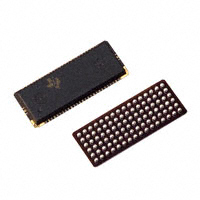
BODY SIZE (NOM)
SN74LVCH32373AG
LFBGA-GKE
KER
13.50 mm × 5.00 mm
SN74LVCH32373AN
LFBGA-NMJ
MJR
13.50 mm × 5.00 mm
(1)
For all available packages, see the orderable addendum at
the end of the data sheet.
One of Four 8-Bit D-Type Latch Banks
xOE
xLE
LE
xD1
Q
xQ1
Q
xQ2
D
Bus-Hold
LE
xD2
D
Bus-Hold
2 Applications
•
•
•
•
PACKAGE(1)
PART NUMBER
xD3
xD4
xD5
xD6
xD7
Buffer registers
I/O ports
Bidirectional bus drivers
Working registers
3 Description
xQ3
xQ4
xQ5
xQ6
xQ7
LE
This 32-bit transparent D-type latch is designed for
1.65-V to 3.6-V VCC operation.
The SN74LVCH32373A is particularly suitable for
implementing buffer registers, I/O ports, bidirectional
bus drivers, and working registers. It can be used as
four 8-bit latches, two 16-bit latches, or one 32-bit
latch. When the latch-enable (LE) input is high, the Q
outputs follow the data (D) inputs. When LE is taken
low, the Q outputs are latched at the levels set up at
the D inputs.
Q
xD8
xQ7
D
Bus-Hold
Logic Diagram
An IMPORTANT NOTICE at the end of this data sheet addresses availability, warranty, changes, use in safety-critical applications,
Submit Document Feedback
Copyright
© 2020 Texas
Instruments
Incorporated
intellectual
property
matters
and other important disclaimers. PRODUCTION DATA.
Product Folder Links: SN74LVCH32373A
1
�SN74LVCH32373A
www.ti.com
SCAS618E – OCTOBER 1998 – REVISED JULY 2020
Table of Contents
1 Features............................................................................1
2 Applications..................................................................... 1
3 Description.......................................................................1
4 Revision History.............................................................. 2
5 Pin Configuration and Functions...................................3
6 Specifications.................................................................. 6
6.1 Absolute Maximum Ratings........................................ 6
6.2 ESD Ratings............................................................... 6
6.3 Recommended Operating Conditions.........................7
6.4 Thermal Information....................................................7
6.5 Electrical Characteristics.............................................8
6.6 Timing Requirements.................................................. 8
6.7 Switching Characteristics............................................9
6.8 Operating Characteristics........................................... 9
6.9 Typical Characteristics................................................ 9
7 Detailed Description...................................................... 11
7.1 Overview................................................................... 11
7.2 Functional Block Diagram......................................... 12
7.3 Feature Description...................................................12
7.4 Device Functional Modes..........................................14
8 Application and Implementation.................................. 15
8.1 Application Information............................................. 15
8.2 Typical Application.................................................... 15
9 Power Supply Recommendations................................17
10 Layout...........................................................................17
10.1 Layout Guidelines................................................... 17
10.2 Layout Example...................................................... 18
11 Device and Documentation Support..........................18
11.1 Documentation Support.......................................... 18
11.2 Support Resources................................................. 18
11.3 Trademarks............................................................. 18
11.4 Electrostatic Discharge Caution.............................. 18
11.5 Glossary.................................................................. 18
12 Mechanical, Packaging, and Orderable
Information.................................................................... 18
4 Revision History
Changes from Revision D (March 2005) to Revision E (July 2020)
Page
• Changed global format to new TI data sheet .....................................................................................................1
• Added Applications list, Device Information table, and key graphic .................................................................. 1
• Added maximum junction temperature .............................................................................................................. 6
• Added ESD Ratings section .............................................................................................................................. 6
• Added Thermal Information section ...................................................................................................................7
• Added Typical Characteristics section ............................................................................................................... 9
• Added Detailed Description section ................................................................................................................. 11
• Added Application and Implementation section ...............................................................................................15
• Added Power Supply Recommendations section and Layout section .............................................................17
2
Submit Document Feedback
Copyright © 2020 Texas Instruments Incorporated
Product Folder Links: SN74LVCH32373A
�SN74LVCH32373A
www.ti.com
SCAS618E – OCTOBER 1998 – REVISED JULY 2020
5 Pin Configuration and Functions
1
2
3
4
5
6
A
1Q2
1Q1
1OE
1LE
1D1
1D2
B
1Q4
1Q3
GND
GND
1D3
1D4
C
1Q6
1Q5
V
V
!
1D5
1D6
D
1Q8
1Q7
GND
GND
1D7
1D8
E
2Q2
2Q1
GND
GND
2D1
2D2
F
2Q4
2Q3
V
V
!
2D3
2D4
G
2Q6
2Q5
GND
GND
2D5
2D6
H
2Q7
2Q8
2OE
2LE
2D8
2D7
J
3Q2
3Q1
3OE
3LE
3D1
3D2
K
3Q4
3Q3
GND
GND
3D3
3D4
L
3Q6
3Q5
V
V
!
3D5
3D6
M
3Q8
3Q7
GND
GND
3D7
3D8
N
4Q2
4Q1
GND
GND
4D1
4D2
P
4Q4
4Q3
V
V
!
4D3
4D4
R
4Q6
4Q5
GND
GND
4D5
4D6
T
4Q7
4Q8
4OE
4LE
4D8
4D7
CC
CC
CC
CC
!
!
!
!
CC
CC
CC
CC
Not to scale
Figure 5-1. GKE 96-Pin LFBGA Transparent Top View
Pin Functions
PIN
NAME
NO.
I/O
DESCRIPTION
1Q2
A1
Output
Bank 1, Channel 2, Q Output
1Q4
B1
Output
Bank 1, Channel 4, Q Output
1Q6
C1
Output
Bank 1, Channel 6, Q Output
1Q8
D1
Output
Bank 1, Channel 8, Q Output
2Q2
E1
Output
Bank 2, Channel 2, Q Output
2Q4
F1
Output
Bank 2, Channel 4, Q Output
2Q6
G1
Output
Bank 2, Channel 6, Q Output
Submit Document Feedback
Copyright © 2020 Texas Instruments Incorporated
Product Folder Links: SN74LVCH32373A
3
�SN74LVCH32373A
www.ti.com
SCAS618E – OCTOBER 1998 – REVISED JULY 2020
PIN
NAME
4
NO.
I/O
DESCRIPTION
2Q7
H1
Output
3Q2
J1
Output
Bank 2, Channel 8, Q Output
Bank 3, Channel 2, Q Output
3Q4
K1
Output
Bank 3, Channel 4, Q Output
3Q6
L1
Output
Bank 3, Channel 6, Q Output
3Q8
M1
Output
Bank 3, Channel 8, Q Output
4Q2
N1
Output
Bank 4, Channel 2, Q Output
4Q4
P1
Output
Bank 4, Channel 4, Q Output
4Q6
R1
Output
Bank 4, Channel 6, Q Output
4Q7
T1
Output
Bank 4, Channel 8, Q Output
1Q1
A2
Output
Bank 1, Channel 1, Q Output
1Q3
B2
Output
Bank 1, Channel 3, Q Output
1Q5
C2
Output
Bank 1, Channel 5, Q Output
1Q7
D2
Output
Bank 1, Channel 7, Q Output
2Q1
E2
Output
Bank 2, Channel 1, Q Output
2Q3
F2
Output
Bank 2, Channel 3, Q Output
2Q5
G2
Output
Bank 2, Channel 5, Q Output
2Q8
H2
Output
Bank 2, Channel 7, Q Output
3Q1
J2
Output
Bank 3, Channel 1, Q Output
3Q3
K2
Output
Bank 3, Channel 3, Q Output
3Q5
L2
Output
Bank 3, Channel 5, Q Output
3Q7
M2
Output
Bank 3, Channel 7, Q Output
4Q1
N2
Output
Bank 4, Channel 1, Q Output
4Q3
P2
Output
Bank 4, Channel 3, Q Output
4Q5
R2
Output
Bank 4, Channel 5, Q Output
4Q8
T2
Output
Bank 4, Channel 7, Q Output
1 OE
A3
Input
GND
B3
—
Ground
Bank 1, Output Enable, Active Low
VCC
C3
—
Positive Supply
GND
D3
—
Ground
GND
E3
—
Ground
VCC
F3
—
Positive Supply
GND
G3
—
Ground
2 OE
H3
Input
3 OE
J3
Input
GND
K3
—
Ground
Bank 2, Output Enable, Active Low
Bank 3, Output Enable, Active Low
VCC
L3
—
Positive Supply
GND
M3
—
Ground
GND
N3
—
VCC
P3
Input
Ground
Positive Supply
GND
R3
—
4 OE
T3
Input
Ground
Bank 4, Output Enable, Active Low
1LE
A4
Input
Bank 1, Latch Enable, Active Low
GND
B4
—
Ground
VCC
C4
—
Positive Supply
GND
D4
—
Ground
Submit Document Feedback
Copyright © 2020 Texas Instruments Incorporated
Product Folder Links: SN74LVCH32373A
�SN74LVCH32373A
www.ti.com
SCAS618E – OCTOBER 1998 – REVISED JULY 2020
PIN
NAME
NO.
I/O
DESCRIPTION
GND
E4
—
Ground
VCC
F4
—
Positive Supply
GND
G4
—
Ground
2LE
H4
Input
Bank 2, Latch Enable, Active Low
3LE
J4
Input
Bank 3, Latch Enable, Active Low
GND
K4
—
Ground
VCC
L4
—
Positive Supply
GND
M4
—
Ground
GND
N4
—
Ground
VCC
P4
—
Positive Supply
GND
R4
—
Ground
4LE
T4
Input
Bank 4, Latch Enable, Active Low
1D1
A5
Input
Bank 1, Channel 1, Data Input
1D3
B5
Input
Bank 1, Channel 3, Data Input
1D5
C5
Input
Bank 1, Channel 5, Data Input
1D7
D5
Input
Bank 1, Channel 7, Data Input
2D1
E5
Input
Bank 2, Channel 1, Data Input
2D3
F5
Input
Bank 2, Channel 3, Data Input
2D5
G5
Input
Bank 2, Channel 5, Data Input
2D8
H5
Input
Bank 2, Channel 8, Data Input
3D1
J5
Input
Bank 3, Channel 1, Data Input
3D3
K5
Input
Bank 3, Channel 3, Data Input
3D5
L5
Input
Bank 3, Channel 5, Data Input
3D7
M5
Input
Bank 3, Channel 7, Data Input
4D1
N5
Input
Bank 4, Channel 1, Data Input
4D3
P5
Input
Bank 4, Channel 3, Data Input
4D5
R5
Input
Bank 4, Channel 5, Data Input
4D8
T5
Input
Bank 4, Channel 8, Data Input
1D2
A6
Input
Bank 1, Channel 2, Data Input
1D4
B6
Input
Bank 1, Channel 4, Data Input
1D6
C6
Input
Bank 1, Channel 6, Data Input
1D8
D6
Input
Bank 1, Channel 8, Data Input
2D2
E6
Input
Bank 2, Channel 2, Data Input
2D4
F6
Input
Bank 2, Channel 4, Data Input
2D6
G6
Input
Bank 2, Channel 6, Data Input
2D7
H6
Input
Bank 2, Channel 7, Data Input
3D2
J6
Input
Bank 3, Channel 2, Data Input
3D4
K6
Input
Bank 3, Channel 4, Data Input
3D6
L6
Input
Bank 3, Channel 6, Data Input
3D8
M6
Input
Bank 3, Channel 8, Data Input
4D2
N6
Input
Bank 4, Channel 2, Data Input
4D4
P6
Input
Bank 4, Channel 4, Data Input
4D6
R6
Input
Bank 4, Channel 6, Data Input
4D7
T6
Input
Bank 4, Channel 7, Data Input
Submit Document Feedback
Copyright © 2020 Texas Instruments Incorporated
Product Folder Links: SN74LVCH32373A
5
�SN74LVCH32373A
www.ti.com
SCAS618E – OCTOBER 1998 – REVISED JULY 2020
6 Specifications
6.1 Absolute Maximum Ratings
over operating free-air temperature range (unless otherwise noted)(1)
VCC
Supply voltage range
range(2)
VI
Input voltage
VO
Voltage range applied to any output in the high-impedance or power-off state(2)
state(2) (3)
MIN
MAX
–0.5
6.5
UNIT
V
–0.5
6.5
V
–0.5
6.5
V
–0.5
VCC + 0.5
VO
Voltage range applied to any output in the high or low
IIK
Input clamp current
VI < 0
–50
mA
IOK
Output clamp current
VO < 0
–50
mA
IO
Continuous output current
±50
mA
±100
mA
TJ
Junction temperature
150
°C
Tstg
Storage temperature range
150
°C
Continuous current through each VCC or GND
(1)
(2)
(3)
–65
V
Stresses beyond those listed under "absolute maximum ratings" may cause permanent damage to the device. These are stress ratings
only, and functional operation of the device at these or any other conditions beyond those indicated under "recommended operating
conditions" is not implied. Exposure to absolute-maximum-rated conditions for extended periods may affect device reliability.
The input negative-voltage and output voltage ratings may be exceeded if the input and output current ratings are observed.
The value of VCC is provided in the recommended operating conditions table.
6.2 ESD Ratings
VALUE
Human-body model (HBM), per ANSI/ESDA/JEDEC
V(ESD)
(1)
(2)
6
Electrostatic discharge
JS-001(1)
Charged-device model (CDM), per JEDEC specification JESD22C101(2)
UNIT
±2000
±1000
V
JEDEC document JEP155 states that 500-V HBM allows safe manufacturing with a standard ESD control process.
JEDEC document JEP157 states that 250-V CDM allows safe manufacturing with a standard ESD control process.
Submit Document Feedback
Copyright © 2020 Texas Instruments Incorporated
Product Folder Links: SN74LVCH32373A
�SN74LVCH32373A
www.ti.com
SCAS618E – OCTOBER 1998 – REVISED JULY 2020
6.3 Recommended Operating Conditions
over operating free-air temperature range (unless otherwise noted)
Operating
VCC
Supply voltage
VIH
High-level input voltage
Data retention only
MIN
MAX
1.65
3.6
1.5
VCC = 1.65 V to 1.95 V
Low-level input voltage
VI
1.7
VCC = 2.7 V to 3.6 V
2
VO
Output voltage
V
0.35 × VCC
VCC = 2.3 V to 2.7 V
0.7
VCC = 2.7 V to 3.6 V
0.8
Input voltage
0
5.5
High or low state
0
VCC
3-state
0
5.5
VCC = 1.65 V
IOH
High-level output current
Low-level output current
Δt/Δv
Input transition rise or fall rate
TA
Operating free-air temperature
V
V
V
–4
VCC = 2.3 V
–8
VCC = 2.7 V
–12
VCC = 3 V
–24
VCC = 1.65 V
IOL
V
0.65 × VCC
VCC = 2.3 V to 2.7 V
VCC = 1.65 V to 1.95 V
VIL
UNIT
mA
4
VCC = 2.3 V
8
VCC = 2.7 V
12
VCC = 3 V
24
–40
mA
10
ns/V
85
°C
6.4 Thermal Information
SN74LVCH32373A
THERMAL
METRIC(1)
GKE
NMJ
96 PINS
96 PINS
UNIT
RθJA
Junction-to-ambient thermal resistance
44.4
26.7
°C/W
RθJC(top)
Junction-to-case (top) thermal resistance
26.1
14.4
°C/W
RθJB
Junction-to-board thermal resistance
23.9
10.7
°C/W
ψJT
Junction-to-top characterization parameter
1.3
1.3
°C/W
ψJB
Junction-to-board characterization parameter
23.8
10.5
°C/W
RθJC(bot)
Junction-to-case (bottom) thermal resistance
N/A
N/A
°C/W
(1)
For more information about traditional and new thermal metrics, see the Semiconductor and IC package thermal metrics application
report.
Submit Document Feedback
Copyright © 2020 Texas Instruments Incorporated
Product Folder Links: SN74LVCH32373A
7
�SN74LVCH32373A
www.ti.com
SCAS618E – OCTOBER 1998 – REVISED JULY 2020
6.5 Electrical Characteristics
over recommended operating free-air temperature range (unless otherwise noted)
PARAMETER
TEST CONDITIONS
IOH = –100 μA
VOH
1.65 V to 3.6 V
1.65 V
1.2
IOH = –8 mA
2.3 V
1.7
2.7 V
2.2
3V
2.4
3V
2.2
IOL = 100 μA
1.65 V to 3.6 V
0.2
1.65 V
0.45
IOL = 8 mA
2.3 V
0.7
IOL = 12 mA
2.7 V
0.4
3V
0.55
IOL = 24 mA
VI = 0 to 5.5 V
3.6 V
VI = 0.58 V
VI = 0.7 V
II(hold)
VI = 0.8 V
μA
75
–75
3.6 V
±500
Ioff
VI or VO = 5.5 V
0
±10
μA
IOZ
VO = 0 to 5.5 V
3.6 V
±10
μA
ΔICC
(3)
45
–45
VI = 0 to 3.6 V(2)
ICC
(1)
(2)
25
3V
VI = 2 V
μA
–25
2.3 V
VI = 1.7 V
V
±5
1.65 V
VI = 1.07 V
UNIT
V
IOH = –24 mA
IOL = 4 mA
II
MAX
VCC – 0.2
IOH = –4 mA
IOH = –12 mA
VOL
MIN TYP(1)
VCC
VI = VCC or GND
3.6 V ≤ VI ≤ 5.5 V(3)
One input at VCC – 0.6 V,
IO = 0
40
3.6 V
Other inputs at VCC or GND
μA
40
2.7 V to 3.6 V
500
μA
Ci
VI = VCC or GND
3.3 V
5
pF
Co
VO = VCC or GND
3.3 V
6.5
pF
All typical values are at VCC = 3.3 V, TA = 25°C.
This is the bus-hold maximum dynamic current. It is the minimum overdrive current required to switch the input from one state to
another.
This applies in the disabled state only.
6.6 Timing Requirements
over recommended operating free-air temperature range (unless otherwise noted) (see Figure 1)
VCC = 1.8 V
± 0.15 V
MIN
MIN
MAX
VCC = 2.7 V
MIN
MAX
VCC = 3.3 V
± 0.3 V
MIN
UNIT
MAX
Pulse duration, LE high
(1)
(1)
3.3
3.3
ns
tsu
Setup time, data before LE↓
(1)
(1)
1.7
1.7
ns
th
Hold time, data after LE↓
(1)
(1)
1.2
1.2
ns
tw
(1)
8
MAX
VCC = 2.5 V
± 0.2 V
This information was not available at the time of publication.
Submit Document Feedback
Copyright © 2020 Texas Instruments Incorporated
Product Folder Links: SN74LVCH32373A
�SN74LVCH32373A
www.ti.com
SCAS618E – OCTOBER 1998 – REVISED JULY 2020
6.7 Switching Characteristics
over operating free-air temperature range (unless otherwise noted)
PARAMETER
tpd
(1)
FROM
(INPUT)
VCC = 1.8 V
± 0.15 V
TO
(OUTPUT)
D
Q
LE
VCC = 2.5 V
± 0.2 V
MIN
MAX
MIN
MAX
(1)
(1)
(1)
(1)
(1)
VCC = 2.7 V
MIN
VCC = 3.3 V
± 0.3 V
MAX
MIN
MAX
(1)
4.9
1.6
4.2
(1)
(1)
5.3
2.1
4.6
UNIT
ns
ten
OE
Q
(1)
(1)
(1)
(1)
5.7
1.3
4.7
ns
tdis
OE
Q
(1)
(1)
(1)
(1)
6.3
2.5
5.9
ns
This information was not available at the time of publication.
6.8 Operating Characteristics
TA = 25°C
TEST
CONDITIONS
PARAMETER
Cpd
(1)
Outputs enabled
Power dissipation capacitance
per latch
Outputs disabled
VCC = 1.8 V
VCC = 2.5 V
VCC = 3.3 V
TYP
TYP
TYP
(1)
(1)
39
(1)
(1)
6
f = 10 MHz
UNIT
pF
This information was not available at the time of publication.
6.9 Typical Characteristics
300
VCC = 3.6 V
VCC = 3.3 V
Input Hold Current, II(hold) ( A)
200
VCC = 3 V
VCC = 2.7 V
100
0
-100
-200
-300
0
1
2
Input Voltage, VI (V)
3
4
Figure 6-1. Typical input current for LVC family bus-hold inputs
Submit Document Feedback
Copyright © 2020 Texas Instruments Incorporated
Product Folder Links: SN74LVCH32373A
9
�SN74LVCH32373A
www.ti.com
SCAS618E – OCTOBER 1998 – REVISED JULY 2020
Parameter Measurement Information
VLOAD
S1
RL
From Output
Under Test
CL
(see Note A)
Open
GND
RL
TEST
S1
tPLH/tPHL
tPLZ/tPZL
tPHZ/tPZH
Open
VLOAD
GND
LOAD CIRCUIT
INPUTS
VCC
1.8 V ± 0.15 V
2.5 V ± 0.2 V
2.7 V
3.3 V ± 0.3 V
VI
tr/tf
VCC
VCC
2.7 V
2.7 V
≤2 ns
≤2 ns
≤2.5 ns
≤2.5 ns
VM
VLOAD
CL
RL
V∆
VCC/2
VCC/2
1.5 V
1.5 V
2 × VCC
2 × VCC
6V
6V
30 pF
30 pF
50 pF
50 pF
1 kΩ
500 Ω
500 Ω
500 Ω
0.15 V
0.15 V
0.3 V
0.3 V
VI
Timing Input
VM
0V
tw
tsu
VI
Input
VM
VM
th
VI
Data Input
VM
VM
0V
0V
VOLTAGE WAVEFORMS
SETUP AND HOLD TIMES
VOLTAGE WAVEFORMS
PULSE DURATION
VI
VM
Input
VM
0V
VOH
VM
Output
VM
VOL
VM
0V
VLOAD/2
VM
tPZH
VOH
Output
VM
tPLZ
Output
Waveform 1
S1 at VLOAD
(see Note B)
tPLH
tPHL
VM
tPZL
tPHL
tPLH
VI
Output
Control
VM
VOL
VOLTAGE WAVEFORMS
PROPAGATION DELAY TIMES
INVERTING AND NONINVERTING OUTPUTS
VOL + V∆
VOL
tPHZ
Output
Waveform 2
S1 at GND
(see Note B)
VM
VOH − V∆
VOH
≈0 V
VOLTAGE WAVEFORMS
ENABLE AND DISABLE TIMES
LOW- AND HIGH-LEVEL ENABLING
NOTES: A. CL includes probe and jig capacitance.
B. Waveform 1 is for an output with internal conditions such that the output is low, except when disabled by the output control.
Waveform 2 is for an output with internal conditions such that the output is high, except when disabled by the output control.
C. All input pulses are supplied by generators having the following characteristics: PRR ≤ 10 MHz, ZO = 50 Ω.
D. The outputs are measured one at a time, with one transition per measurement.
E. tPLZ and tPHZ are the same as tdis.
F. tPZL and tPZH are the same as ten.
G. tPLH and tPHL are the same as tpd.
H. All parameters and waveforms are not applicable to all devices.
Figure 7-1. Load Circuit and Voltage Waveforms
10
Submit Document Feedback
Copyright © 2020 Texas Instruments Incorporated
Product Folder Links: SN74LVCH32373A
�SN74LVCH32373A
www.ti.com
SCAS618E – OCTOBER 1998 – REVISED JULY 2020
7 Detailed Description
7.1 Overview
The SN74LVCH32373A is a 32-bit transparent D-type latch that is designed for 1.65-V to 3.6-V VCC operation.
A buffered output-enable (OE) input can be used to place the eight outputs in either a normal logic state (high or
low logic levels) or the high-impedance state. In the high-impedance state, the outputs neither load nor drive the
bus lines significantly. The high-impedance state and increased drive provide the capability to drive bus lines
without interface or pullup components.
OE does not affect internal operations of the latch. Old data can be retained or new data can be entered while
the outputs are in the high-impedance state.
Inputs can be driven from either 3.3-V or 5-V devices. This feature allows the use of these devices as translators
in a mixed 3.3-V/5-V system environment.
This device is fully specified for partial-power-down applications using Ioff. The Ioff circuitry disables the outputs,
preventing damaging current backflow through the device when it is powered down.
To ensure the high-impedance state during power up or power down, OE should be tied to VCC through a pull-up
resistor; the minimum value of the resistor is determined by the current-sinking capability of the driver.
Active bus-hold circuitry holds unused or undriven inputs at a valid logic state. Use of pull-up or pull-down
resistors with the bus-hold circuitry is not recommended.
Latches are arranged in banks of 8, with each bank having a separate latch enable (LE) and output enable ( OE)
associated with it, as shown in the functional block diagram below.
When the latch enable pin for a bank is asserted (HIGH), the outputs will follow the data inputs.
When the latch enable pin for a bank is de-asserted (LOW), the outputs will continue to hold the valid input value
at the time of switching.
When the output enable pin is asserted (LOW), the output is active.
When the output enable pin is de-asserted (HIGH), the output is disabled (high impedance). This does not affect
the latch operation.
Submit Document Feedback
Copyright © 2020 Texas Instruments Incorporated
Product Folder Links: SN74LVCH32373A
11
�SN74LVCH32373A
www.ti.com
SCAS618E – OCTOBER 1998 – REVISED JULY 2020
7.2 Functional Block Diagram
One of Four 8-Bit D-Type Latch Banks
xOE
xLE
LE
xD1
Q
xQ1
Q
xQ2
D
Bus-Hold
LE
xD2
D
Bus-Hold
xD3
xD4
xD5
xD6
xD7
xQ3
xQ4
xQ5
xQ6
xQ7
LE
Q
xD8
xQ7
D
Bus-Hold
7.3 Feature Description
7.3.1 Standard CMOS Inputs
Standard CMOS inputs are high impedance and are typically modeled as a resistor in parallel with the input
capacitance to ground given in the Electrical Characteristics. The worst case resistance is calculated with the
maximum input voltage, given in the Absolute Maximum Ratings, and the maximum input leakage current, given
in the Electrical Characteristics, using ohm's law (R = V ÷ I).
Signals applied to the inputs need to have fast edge rates, as defined by Δt/Δv in the Recommended Oeprating
Conditions to avoid excessive current consumption and oscillations. If a slow or noisy input signal is required, a
device with a Schmitt-trigger input should be used to condition the input signal prior to the standard CMOS input.
7.3.2 Balanced High-Drive CMOS Push-Pull Outputs
A balanced output allows the device to sink and source similar currents. The high drive capability of this device
creates fast edges into light loads so routing and load conditions should be considered to prevent ringing.
Additionally, the outputs of this device are capable of driving larger currents than the device can sustain without
being damaged. The electrical and thermal limits defined in the Absolute Maximum Ratings must be followed at
all times.
7.3.3 Partial Power Down (Ioff)
The inputs and outputs for this device enter a high-impedance state when the device is powered down, inhibiting
current backflow into the device. The maximum leakage into or out of any input or output pin on the device is
specified by Ioff in the Electrical Characteristics.
12
Submit Document Feedback
Copyright © 2020 Texas Instruments Incorporated
Product Folder Links: SN74LVCH32373A
�SN74LVCH32373A
www.ti.com
SCAS618E – OCTOBER 1998 – REVISED JULY 2020
7.3.4 Over-voltage Tolerant Inputs
Input signals to this device can be driven above the supply voltage so long as they remain below the maximum
input voltage value specified in the Recommended Operating Conditions.
7.3.5 Clamp Diode Structure
The inputs and outputs to this device have negative clamping diodes only as depicted in Figure 7-1.
CAUTION
Voltages beyond the values specified in the Absolute Maximum Ratings table can cause damage to
the device. The input negative-voltage and output voltage ratings may be exceeded if the input and
output clamp-current ratings are observed.
Device
VCC
Logic
Input
Output
-IIK
-IOK
GND
Figure 7-1. Electrical Placement of Clamping Diodes for Each Input and Output
7.3.6 Bus-Hold Data Inputs
Each data input (D) on this device includes a weak latch that maintains a valid logic level on the input. The state
of these latches is unknown at startup and remains unknown until the input has been forced to a valid high or
low state. After data has been sent through a channel, the latch then maintains the previous state on the input if
the line is left floating. It is not recommended to use pull-up or pull-down resistors together with a bus-hold input,
as it may cause undefined inputs to occur which can lead to excessive current consumption.
Bus-hold data inputs prevent floating inputs on this device. The Implications of Slow or Floating CMOS Inputs
application report explains the problems associated with leaving CMOS inputs floating. These latches remain
active at all times, independent of all control signals such as direction control or output enable. The Bus-Hold
Circuit application report has additional details regarding bus-hold inputs.
Input
Logic
Output
Bus-Hold Latch
Figure 7-2. Bus-Hold circuit block diagram representation
Submit Document Feedback
Copyright © 2020 Texas Instruments Incorporated
Product Folder Links: SN74LVCH32373A
13
�SN74LVCH32373A
www.ti.com
SCAS618E – OCTOBER 1998 – REVISED JULY 2020
7.4 Device Functional Modes
Table 7-1. Function Table
INPUTS
1OE
OE
LE
D
OUTPUT
Q
L
H
H
H
L
H
L
L
L
L
X
Q0
H
X
X
Z
A3
2OE
A4
H4
1LE
2LE
C1
1D1
H3
A5
C1
A2
1Q1
1D
2D1
E5
To Seven Other Channels
3OE
2Q1
To Seven Other Channels
J3
4OE
J4
T3
T4
3LE
4LE
C1
3D1
E2
1D
J5
C1
J2
3Q1
1D
To Seven Other Channels
4D1
N5
1D
N2
4Q1
To Seven Other Channels
Figure 7-3. Logic Diagram (Positive Logic)
14
Submit Document Feedback
Copyright © 2020 Texas Instruments Incorporated
Product Folder Links: SN74LVCH32373A
�SN74LVCH32373A
www.ti.com
SCAS618E – OCTOBER 1998 – REVISED JULY 2020
8 Application and Implementation
Note
Information in the following applications sections is not part of the TI component specification, and TI
does not warrant its accuracy or completeness. TI’s customers are responsible for determining
suitability of components for their purposes. Customers should validate and test their design
implementation to confirm system functionality.
8.1 Application Information
In this application, the SN74LVCH32373A 32-bit D-type latch with bus-hold inputs is used to control a 24-bit bus.
8.2 Typical Application
VCC
VCC
VCC
VCC
1OE
2OE
Bypass capacitors placed
one per supply pin
Each 0.022 F
3OE
24-Bit
Data
Source
24
4OE
8
8
8
Unused data
inputs not
connected
Bus
Controller
8
1D[1-8]
2D[1-8]
3D[1-8]
1Q[1-8]
4D[1-8]
2Q[1-8]
1LE
3Q[1-8]
2LE
4Q[1-8]
8
24-Bit
Bus
8
8
8
3LE
4LE
24
Unused
outputs not
connected
GND
Figure 8-1. Simplified schematic for typical application
8.2.1 Design Requirements
•
•
All signals in the system operate at the same voltage within the recommended operating range of the device
Inputs can be disconnected or placed into the high-impedance state; bus-hold circuitry will maintain the last
known state at the input
• Outputs must remain active at all times to prevent the bus from floating
8.2.1.1 Power Considerations
Ensure the desired supply voltage is within the range specified in the Recommended Operating Conditions. The
supply voltage sets the device's electrical characteristics as described in the Electrical Characteristics.
The supply must be capable of sourcing current equal to the total current to be sourced by all outputs of the
SN74LVCH32373A plus the maximum supply current, ICC, listed in the Electrical Characteristics. The logic
device can only source or sink as much current as it is provided at the supply and ground pins, respectively. Be
sure not to exceed the maximum total current through GND or VCC listed in the Absolute Maximum Ratings.
Submit Document Feedback
Copyright © 2020 Texas Instruments Incorporated
Product Folder Links: SN74LVCH32373A
15
�SN74LVCH32373A
www.ti.com
SCAS618E – OCTOBER 1998 – REVISED JULY 2020
The SN74LVCH32373A can drive a load with a total capacitance less than or equal to 50 pF connected to a
high-impedance CMOS input while still meeting all of the datasheet specifications. Larger capacitive loads can
be applied, however it is not recommended to exceed 70 pF.
Total power consumption can be calculated using the information provided in CMOS Power Consumption and
Cpd Calculation.
Thermal increase can be calculated using the information provided in Thermal Characteristics of Standard Linear
and Logic (SLL) Packages and Devices.
CAUTION
The maximum junction temperature, TJ(max) listed in the Absolute Maximum Ratings, is an
additional limitation to prevent damage to the device. Do not violate any values listed in the Absolute
Maximum Ratings. These limits are provided to prevent damage to the device.
8.2.1.2 Input Considerations
Unused inputs must be terminated to either VCC or ground. These can be directly terminated if the input is
completely unused, or they can be connected with a pull-up or pull-down resistor if the input is to be used
sometimes, but not always. A pull-up resistor is used for a default state of HIGH, and a pull-down resistor is used
for a default state of LOW. The resistor size is limited by drive current of the controller, leakage current into the
SN74LVCH32373A, as specified in the Electrical Characteristics, and the desired input transition rate. A 10-kΩ
resistor value is often used due to these factors.
The SN74LVCH32373A has standard CMOS inputs, so input signal edge rates cannot be slow. Slow input edge
rates can cause oscillations and damaging shoot-through current. The recommended rates are defined in the
Recommended Operating Conditions.
Refer to the Feature Description for additional information regarding the inputs for this device.
8.2.1.3 Output Considerations
The positive supply voltage is used to produce the output HIGH voltage. Drawing current from the output will
decrease the output voltage as specified by the VOH specification in the Electrical Characteristics. Similarly, the
ground voltage is used to produce the output LOW voltage. Sinking current into the output will increase the
output voltage as specified by the VOL specification in the Electrical Characteristics. The plots in Figure 8-2 and
Figure 8-3 provide a typical relationship between output voltage and current for this device.
Unused outputs can be left floating.
Refer to Feature Description for additional information regarding the outputs for this device.
8.2.1.4 Timing Considerations
The SN74LVCH32373A is a latched device. As such, it requires special timing considerations to ensure normal
operation.
Primary timing factors to consider:
•
Pulse duration: ensure that the triggering event duration is larger than the minimum pulse duration, as
defined in the Timing Requirements.
• Setup time: ensure that the data has changed at least one setup time prior to the triggering event, as defined
in the Timing Requirements.
• Hold time: ensure that the data remains in the desired state at least one hold time after the triggering event,
as defined in the Timing Requirements.
8.2.2 Detailed Design Procedure
1. Add a decoupling capacitor from each supply pin (VCC) to a nearby GND pin. The capacitor needs to be
placed physically close to the device and electrically close to both the VCC and GND pins. For BGA type
packages, these capacitors are often placed on the back of the board to minimize trace length. Adding one
capacitor per supply pin is recommended.
16
Submit Document Feedback
Copyright © 2020 Texas Instruments Incorporated
Product Folder Links: SN74LVCH32373A
�SN74LVCH32373A
www.ti.com
SCAS618E – OCTOBER 1998 – REVISED JULY 2020
2. Ensure the capacitive load at the output is ≤ 70 pF. This is not a hard limit, however it will ensure optimal
performance. This can be accomplished by providing short, appropriately sized traces from the
SN74LVCH32373A to the receiving device.
3. Ensure the resistive load at the output is larger than (VCC / 50 mA) Ω. This will ensure that the maximum
output current from the Absolute Maximum Ratings is not violated. Most CMOS inputs have a resistive load
measured in megaohms; much larger than the minimum calculated above.
4. Thermal issues are rarely a concern for logic gates, however the power consumption and thermal increase
can be calculated using the steps provided in the application report, CMOS Power Consumption and Cpd
Calculation. In multi-channel high-speed applications, it is possible to reach the thermal limits of the device
without violating any other absolute maximum ratings.
0
100
-6
90
-12
80
-18
70
-24
60
IOL (mA)
IOH (mA)
8.2.3 Application Curves
-30
-36
50
40
-42
30
-48
20
-54
10
0
-60
0
0.3
0.6
0.9
1.2
1.5 1.8
VOH (V)
2.1
2.4
2.7
3
0
0.2
0.4
typ_
0.6
0.8
VOL (V)
1
1.2
1.4
1.6
typ_
Figure 8-2. LVC family typical output voltage in the Figure 8-3. LVC family typical output voltage in the
low state
high state
9 Power Supply Recommendations
The power supply can be any voltage between the minimum and maximum supply voltage rating located in the
Recommended Operating Conditions. Each VCC terminal should have a good bypass capacitor to prevent power
disturbance. A 0.022-μF capacitor at each supply pin is recommended for this device. It is acceptable to parallel
multiple bypass caps to reject different frequencies of noise. The bypass capacitor should be installed as close
to the power terminal as possible for best results. With BGA packages, this often means putting the capacitors
on the back of the board.
10 Layout
10.1 Layout Guidelines
When using multiple-input and multiple-channel logic devices inputs must not ever be left floating. In many
cases, functions or parts of functions of digital logic devices are unused; for example, when only 24 channels of
a 32-channel D-type latch are used. Pins with bus-hold circuitry (xDy) are automatically held in a valid state and
can be left unconnected without the input voltage floating. Other inputs, such as the xLE and x OE must be
terminated at either ground or VCC to prevent floating. Generally, the inputs are tied to GND or VCC, whichever
makes more sense for the logic function or is more convenient.
It is not recommended to use pull-up or pull-down resistors with bus-hold inputs.
Submit Document Feedback
Copyright © 2020 Texas Instruments Incorporated
Product Folder Links: SN74LVCH32373A
17
�SN74LVCH32373A
www.ti.com
SCAS618E – OCTOBER 1998 – REVISED JULY 2020
10.2 Layout Example
0.8mm
pitch
0.350mm
Dia. Pad
0.50mm dia.
solder mask
opening
0.125mm
Trace
0.254mm
dia. hole
Figure 10-1. BGA layout examples
11 Device and Documentation Support
11.1 Documentation Support
11.1.1 Related Documentation
For related documentation see the following:
•
•
CMOS Power Consumption and CPD Calculation
Designing with Logic
11.2 Support Resources
TI E2E™ support forums are an engineer's go-to source for fast, verified answers and design help — straight
from the experts. Search existing answers or ask your own question to get the quick design help you need.
Linked content is provided "AS IS" by the respective contributors. They do not constitute TI specifications and do
not necessarily reflect TI's views; see TI's Terms of Use.
11.3 Trademarks
Widebus+™ is a trademark of Texas Instruments.
TI E2E™ is a trademark of Texas Instruments.
All other trademarks are the property of their respective owners.
11.4 Electrostatic Discharge Caution
This integrated circuit can be damaged by ESD. Texas Instruments recommends that all integrated circuits be handled
with appropriate precautions. Failure to observe proper handling and installation procedures can cause damage.
ESD damage can range from subtle performance degradation to complete device failure. Precision integrated circuits may
be more susceptible to damage because very small parametric changes could cause the device not to meet its published
specifications.
11.5 Glossary
TI Glossary
This glossary lists and explains terms, acronyms, and definitions.
12 Mechanical, Packaging, and Orderable Information
The following pages include mechanical, packaging, and orderable information. This information is the most
current data available for the designated devices. This data is subject to change without notice and revision of
this document. For browser-based versions of this data sheet, refer to the left-hand navigation.
18
Submit Document Feedback
Copyright © 2020 Texas Instruments Incorporated
Product Folder Links: SN74LVCH32373A
�PACKAGE OPTION ADDENDUM
www.ti.com
26-May-2021
PACKAGING INFORMATION
Orderable Device
Status
(1)
Package Type Package Pins Package
Drawing
Qty
Eco Plan
(2)
Lead finish/
Ball material
MSL Peak Temp
Op Temp (°C)
Device Marking
(3)
(4/5)
(6)
SN74LVCH32373ANMJR
ACTIVE
NFBGA
NMJ
96
1000
RoHS & Green
SNAGCU
Level-3-260C-168 HR
-40 to 85
29TW
(1)
The marketing status values are defined as follows:
ACTIVE: Product device recommended for new designs.
LIFEBUY: TI has announced that the device will be discontinued, and a lifetime-buy period is in effect.
NRND: Not recommended for new designs. Device is in production to support existing customers, but TI does not recommend using this part in a new design.
PREVIEW: Device has been announced but is not in production. Samples may or may not be available.
OBSOLETE: TI has discontinued the production of the device.
(2)
RoHS: TI defines "RoHS" to mean semiconductor products that are compliant with the current EU RoHS requirements for all 10 RoHS substances, including the requirement that RoHS substance
do not exceed 0.1% by weight in homogeneous materials. Where designed to be soldered at high temperatures, "RoHS" products are suitable for use in specified lead-free processes. TI may
reference these types of products as "Pb-Free".
RoHS Exempt: TI defines "RoHS Exempt" to mean products that contain lead but are compliant with EU RoHS pursuant to a specific EU RoHS exemption.
Green: TI defines "Green" to mean the content of Chlorine (Cl) and Bromine (Br) based flame retardants meet JS709B low halogen requirements of


 工商网监
湘ICP备2023018690号
工商网监
湘ICP备2023018690号
