SN74LVCZ161284A
19-BIT IEEE STD 1284 TRANSLATION TRANSCEIVER
WITH ERROR-FREE POWER UP
www.ti.com
SCES358B – SEPTEMBER 2001 – REVISED MAY 2005
FEATURES
•
•
•
•
•
•
•
•
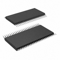
DGG PACKAGE
(TOP VIEW)
Power-On Reset (POR) Prevents Printer
Errors When Printer Is Turned On, But No
Valid Signal Is at Pins A9–A13
Operates From 3 V to 3.6 V
1.4-kΩ Pullup Resistors Integrated on All
Open-Drain Outputs Eliminate the Need for
Discrete Resistors
Designed for IEEE Std 1284-I (Level-1 Type)
and IEEE Std 1284-II (Level-2 Type) Electrical
Specifications
Flow-Through Architecture Optimizes PCB
Layout
Ioff and Power-Up 3-State Support Hot
Insertion
Latch-Up Performance Exceeds 100 mA Per
JESD 78, Class II
ESD Protection Exceeds JESD 22
– 4000-V Human-Body Model (A114-A)
– 350-V Machine Model (A115-A)
– 1500-V Charged-Device Model (C101)
DESCRIPTION/ORDERING INFORMATION
The SN74LVCZ161284A is designed for 3-V to 3.6-V
VCC operation. This device provides asynchronous
two-way communication between data buses. The
control-function implementation minimizes external
timing requirements.
HD
A9
A10
A11
A12
A13
VCC
A1
A2
GND
A3
A4
A5
A6
GND
A7
A8
VCC
PERI LOGIC IN
A14
A15
A16
A17
HOST LOGIC OUT
1
48
2
47
3
46
4
45
5
44
6
43
7
42
8
41
9
40
10
39
11
38
12
37
13
36
14
35
15
34
16
33
17
32
18
31
19
30
20
29
21
28
22
27
23
26
24
25
DIR
Y9
Y10
Y11
Y12
Y13
VCC CABLE
B1
B2
GND
B3
B4
B5
B6
GND
B7
B8
VCC CABLE
PERI LOGIC OUT
C14
C15
C16
C17
HOST LOGIC IN
This device has eight bidirectional bits; data can flow in the A-to-B direction when the direction-control (DIR) input
is high and in the B-to-A direction when DIR is low. This device also has five drivers that drive the cable side and
four receivers. The SN74LVCZ161284A has one receiver dedicated to the HOST LOGIC line and a driver to
drive the PERI LOGIC line.
The output drive mode is determined by the high-drive (HD) control pin. When HD is high, the outputs are in a
totem-pole configuration and in an open-drain configuration when HD is low. This meets the drive requirements
as specified in the IEEE Std 1284-I (level-1 type) and IEEE Std 1284-II (level-2 type) parallel peripheral-interface
specifications. Except for HOST LOGIC IN and peripheral logic out (PERI LOGIC OUT), all cable-side pins have
a 1.4-kΩ integrated pullup resistor. The pullup resistor is switched off if the associated output driver is in the low
state or if the output voltage is above VCC CABLE. If VCC CABLE is off, PERI LOGIC OUT is set to low.
The device has two supply voltages. VCC is designed for 3-V to 3.6-V operation. VCC CABLE supplies the inputs
and output buffers of the cable side only and is designed for 3-V to 3.6-V and for 4.7-V to 5.5-V operation. Even
when VCC CABLE is 3 V to 3.6 V, the cable-side I/O pins are 5-V tolerant.
ORDERING INFORMATION
PACKAGE (1)
TA
0°C to 70°C
(1)
TSSOP – DGG
Tape and reel
ORDERABLE PART NUMBER
SN74LVCZ161284AGR
TOP-SIDE MARKING
LVCZ161284A
Package drawings, standard packing quantities, thermal data, symbolization, and PCB design guidelines are available at
www.ti.com/sc/package.
Please be aware that an important notice concerning availability, standard warranty, and use in critical applications of Texas
Instruments semiconductor products and disclaimers thereto appears at the end of this data sheet.
PRODUCTION DATA information is current as of publication date.
Products conform to specifications per the terms of the Texas
Instruments standard warranty. Production processing does not
necessarily include testing of all parameters.
Copyright © 2001–2005, Texas Instruments Incorporated
�SN74LVCZ161284A
19-BIT IEEE STD 1284 TRANSLATION TRANSCEIVER
WITH ERROR-FREE POWER UP
www.ti.com
SCES358B – SEPTEMBER 2001 – REVISED MAY 2005
DESCRIPTION/ORDERING INFORMATION (CONTINUED)
The power-on reset (POR) ensures that the Y outputs (Y9–Y13) stay in the high state after power on until an
associated input (A9–A13) goes high. When an associated input goes high, all Y outputs are activated, and
noninverting signals of the associated inputs are driven through Y outputs. This special feature prevents printer
system errors caused by deasserting the BUSY signal in the cable at power on.
FUNCTION TABLE
INPUTS
2
DIR
HD
L
L
L
H
H
L
H
H
OUTPUT
MODE
Open drain
A9–A13 to Y9–Y13 and PERI LOGIC IN to PERI LOGIC OUT
Totem pole
B1–B8 to A1–A8 and C14–C17 to A14–A17
Totem pole
B1–B8 to A1–A8, A9–A13 to Y9–Y13, PERI LOGIC IN to PERI LOGIC OUT, and C14–C17 to A14–A17
Open drain
A1–A8 to B1–B8, A9–A13 to Y9–Y13, and PERI LOGIC IN to PERI LOGIC OUT
Totem pole
C14–C17 to A14–A17
Totem pole
A1–A8 to B1–B8, A9–A13 to Y9–Y13, C14–C17 to A14–A17, and PERI LOGIC IN to PERI LOGIC OUT
�SN74LVCZ161284A
19-BIT IEEE STD 1284 TRANSLATION TRANSCEIVER
WITH ERROR-FREE POWER UP
www.ti.com
SCES358B – SEPTEMBER 2001 – REVISED MAY 2005
LOGIC DIAGRAM
VCC CABLE
DIR
HD
42
See Note A
48
See Note A
1
See Note B
B1–B8
A1–A8
A9–A13
Y9–Y13
See
Note C
PERI LOGIC IN
19
30
C14–C17
A14–A17
HOST LOGIC OUT
PERI LOGIC OUT
24
25
HOST LOGIC IN
NOTES: A. The PMOS transistors prevent backdriving current from the signal pins to VCC CABLE when VCC CABLE is open or at GND. The
PMOS transistor is turned off when the associated driver is in the low state.
B. The PMOS transistor prevents backdriving current from the signal pins to VCC CABLE when VCC CABLE is open or at GND.
C. Active input detection circuit forces Y9–Y13 to the high state after power on, until one of the A9–A13 pins goes high (see below).
D
A9
A10
A11
A12
A13
Timer
Q
OUT
C
R
Power-On
Reset
Active Input Detection Circuit
3
�SN74LVCZ161284A
19-BIT IEEE STD 1284 TRANSLATION TRANSCEIVER
WITH ERROR-FREE POWER UP
www.ti.com
SCES358B – SEPTEMBER 2001 – REVISED MAY 2005
Absolute Maximum Ratings (1)
over operating free-air temperature range (unless otherwise noted)
MIN
MAX
VCC CABLE
Supply voltage range
–0.5
7
V
VCC
Supply voltage range
–0.5
4.6
V
Cable
side (2) (3)
–2
7
–0.5
VCC + 0.5
UNIT
VI
VO
Input and output voltage range
IIK
Input clamp current
VI < 0
–20
mA
IOK
Output clamp current
VO < 0
–50
mA
Except PERI LOGIC OUT
±50
IO
Continuous output current
Peripheral side (2)
PERI LOGIC OUT
Output high sink current
θJA
Package thermal impedance (4)
Tstg
Storage temperature range
(1)
(2)
(3)
(4)
mA
±100
Continuous current through each VCC or GND
ISK
V
±200
VO = 5.5 V and VCC CABLE = 3 V
–65
mA
65
mA
70
°C/W
150
°C
Stresses beyond those listed under "absolute maximum ratings" may cause permanent damage to the device. These are stress ratings
only, and functional operation of the device at these or any other conditions beyond those indicated under "recommended operating
conditions" is not implied. Exposure to absolute-maximum-rated conditions for extended periods may affect device reliability.
The input and output voltage ratings may be exceeded if the input and output current ratings are observed.
The ac input voltage pulse duration is limited to 40 ns if the amplitude is greater than –0.5 V.
The package thermal impedance is calculated in accordance with JESD 51-7.
Recommended Operating Conditions (1)
MIN
MAX
UNIT
VCC CABLE
Supply voltage for the cable side, VCC CABLE ≥ VCC
3
5.5
V
VCC
Supply voltage
3
3.6
V
A, B, DIR, and HD
VIH
High-level input voltage
C14–C17
2.3
HOST LOGIC IN
2.6
PERI LOGIC IN
VIL
Low-level input voltage
VI
Input voltage
VO
Open-drain output voltage
IOH
High-level output current
2
2
A, B, DIR, and HD
0.8
C14–C17
0.8
HOST LOGIC IN
1.6
PERI LOGIC IN
0.8
Peripheral side
0
VCC
Cable side
0
5.5
HD low
0
5.5
HD high, B and Y outputs
–4
(1)
4
Operating free-air temperature
V
mA
14
A outputs and HOST LOGIC OUT
4
PERI LOGIC OUT
TA
V
–0.5
B and Y outputs
Low-level output current
V
–14
A outputs and HOST LOGIC OUT
PERI LOGIC OUT
IOL
V
mA
84
0
70
All unused inputs of the device must be held at VCC or GND to ensure proper device operation. Refer to the TI application report,
Implications of Slow or Floating CMOS Inputs, literature number SCBA004.
°C
�SN74LVCZ161284A
19-BIT IEEE STD 1284 TRANSLATION TRANSCEIVER
WITH ERROR-FREE POWER UP
www.ti.com
SCES358B – SEPTEMBER 2001 – REVISED MAY 2005
Electrical Characteristics
over recommended operating free-air temperature range, VCC CABLE = 5 V (unless otherwise noted)
PARAMETER
∆Vt
Hysteresis
(VT+ – VT–)
VOH
VOL
IOH = –14 mA
HD high, A outputs, and
HOST LOGIC OUT
IOH = –4 mA
PERI LOGIC OUT
IOH = –0.5 mA
B and Y outputs
IOL = 14 mA
Ioff
UNIT
V
0.2
3V
2.23
3.3 V (2)
2.4
3V
IOH = –50 µA
2.4
3.15 V
3.1
V (2)
4.5
3.3
V
2.8
0.77
IOL = 50 µA
0.2
3V
IOL = 4 mA
04
IOL = 84 mA
V
0.9
VI = VCC
50
µA
–3.5
mA
VI = VCC or GND
3.6 V
±1
µA
A1–A8
VO = VCC or GND
3.6 V
±20
µA
VO = VCC CABLE
3.6 V
50
µA
VO = GND (pullup resistors)
3.6
V (3)
–3.5
mA
VO = GND (pullup resistors)
3.6 V (3)
–3.5
mA
350
µA
–5
mA
B and Y outputs
B and Y outputs
VI = GND (pullup resistors)
3.6 V (3)
All inputs except B or C inputs
Open-drain Y outputs
IOZPD
MAX
0.8
HD high, B and Y outputs
B outputs
IOZPU
3.3 V
C inputs
C inputs
MIN TYP (1)
0.4
HOST LOGIC IN
PERI LOGIC OUT
IOZ
VCC
All inputs except
C inputs and HOST LOGIC IN
A outputs and HOST LOGIC OUT
II
TEST CONDITIONS
VO = 5.5 V
0 to 1.5 V (4)
VO = GND
VO = 5.5 V
0 to 1.5 V (4)
VO = GND
Power-down input leakage,
except A1–A8 or B1–B8 inputs
VI or VO = 0 to 3.6 V
Power-down output leakage,
B1–B8 and Y9–Y13 outputs
VI or VO = 0 to 5.5 V
µA
–5
mA
100
µA
0 (3)
100
3.6 V (5)
VI = GND (12 × pullup)
ICC
350
VI = VCC,
IO = 0
45
3.6 V
70
3.6 V
0.8
mA
Ci
All inputs
VI = VCC or GND
3.3 V
3
pF
Cio
I/O ports
VO = VCC or GND
3.3 V
7
pF
ZO
Cable side
IOH = –35 mA
3.3 V
45
R pullup
Cable side
VO = 0 V (in high-impedance state)
3.3 V
(1)
(2)
(3)
(4)
(5)
1.15
Ω
1.65
kΩ
Typical values are measured at VCC = 3.3 V, VCC CABLE = 5 V, and TA = 25°C.
VCC CABLE = 4.7 V
VCC CABLE = 3.6 V
Connect the VCC pin and the VCC CABLE pin.
VCC CABLE = 4.7 V
5
�SN74LVCZ161284A
19-BIT IEEE STD 1284 TRANSLATION TRANSCEIVER
WITH ERROR-FREE POWER UP
www.ti.com
SCES358B – SEPTEMBER 2001 – REVISED MAY 2005
Switching Characteristics
over recommended ranges of supply voltage and operating free-air temperature (unless otherwise noted) (see Figure 2 and
Figure 3)
FROM
(INPUT)
TO
(OUTPUT)
Totem pole
A1–A8
B1–B8
Totem pole
A9–A13
Y9–Y13
Totem pole
B1–B8
A1–A8
Totem pole
C14–C17
A14–A17
Totem pole
PERI LOGIC IN
PERI LOGIC OUT
Totem pole
HOST LOGIC IN
HOST LOGIC OUT
PARAMETER
tPLH
tPHL
tPLH
tPHL
tPLH
tPHL
tPLH
tPHL
tPLH
tPHL
tPLH
tPHL
tslew
Totem pole
B1–B8 and Y9–Y13 outputs
tPZH
tPHZ
ten–tdis
tPHZ
tPLZ
tr, tf
Open drain
tsk(o) (2)
(1)
(2)
MIN TYP (1) MAX
1
22
1
22
1
20
1
20
1
10
1
10
1
11
1
11
1
13
1
13
1
13
1
13
0.05
0.4
20
HD
B1–B8, Y9–Y13, and
PERI LOGIC OUT
1
1
15
DIR
A1–A8
1
15
1
15
1
15
DIR
B1–B8
A1–A13
B1–B8 or Y9–Y13
A1–A8 or B1–B8
B1–B8 or A1–A8
1
2.5
UNIT
ns
ns
ns
ns
ns
ns
V/ns
ns
ns
ns
120
ns
10
ns
Typical values are measured at VCC = 3.3 V, VCC CABLE = 5 V, and TA = 25°C.
Skew is measured at 1/2 (VOH + VOL) for signals switching in the same direction.
Operating Characteristics
VCC = 3.3 V, TA = 25°C
PARAMETER
Cpd
Power dissipation capacitance
VCC = 3.3 V
VCC CABLE = 5 V
TA = 25°C
TYP = 80 ns
TEST CONDITIONS
Outputs enabled
CL = 0,
f = 10 MHz
TYP
UNIT
45
pF
VCC and VCC CABLE
An (one of A9–A13)
50% VCC
Initial Activation Time
Y9–Y13, Other Than Yn
50% VCC CABLE
One of pins A9–A13 is switched as shown above, and the other four inputs are forced at low state.
Figure 1. Error-Free Circuit Timing
6
�SN74LVCZ161284A
19-BIT IEEE STD 1284 TRANSLATION TRANSCEIVER
WITH ERROR-FREE POWER UP
www.ti.com
SCES358B – SEPTEMBER 2001 – REVISED MAY 2005
PARAMETER MEASUREMENT INFORMATION
VCC CABLE
CL = 50 pF
(see Note A)
62 Ω
TP1
2.7 V
Input
(see Note B)
0V
tf1
Sink Load
From
B or Y Output
Under Test
95% (VCC CABLE = 5 V�0.5 V)
50% (VCC CABLE = 5 V�0.5 V)
Output
(see Note B)
tr1
Source Load
CL = 50 pF
(see Note A)
62 Ω
Output
(see Note B)
1.9 V (VCC CABLE = 5 V�0.5 V)
0.4 V
VOLTAGE WAVEFORMS MEASURED AT TP1
SLEW RATE WAVEFORMS (B8−B1 AND Y13−Y9)
SLEW RATE A-TO-B OR A-TO-Y LOAD (TOTEM POLE)
VCC CABLE
2.7 V
Input
(see Note C)
TP1
1.4 V
1.4 V
0V
500 Ω
From
B or Y Output
CL = 50 pF
(see Note A)
2V
Output
(see Note C)
VOH
2V
0.8 V
0.8 V
tr
VOL
tf
VOLTAGE WAVEFORMS MEASURED AT TP1, B SIDE
A-TO-B LOAD OR A-TO-Y LOAD (OPEN DRAIN)
NOTES: A. CL includes probe and jig capacitance.
B. When VCC CABLE is 3.3 V � 0.3 V, slew rate is measured between 0.4 V and 0.9 V for the rising edge and between 2.4 V and
1.9 V for the falling edge. When VCC CABLE is 5 V � 0.5 V, slew rate is measured between 0.4 V and 1.9 V for the rising edge and
between 95% VCC CABLE and 50% VCC CABLE for the falling edge.
�
�
tslew fall � VCC 95% � 50%
t f1
C.
D.
E.
F.
G.
�
�
tslew rise � 1.9 V – 0.4 V
tr1
Input rise (tr) and fall (tf) times are 3 ns. Rise and fall times (open drain) are


 工商网监
湘ICP备2023018690号
工商网监
湘ICP备2023018690号
