�������� ��
� �������� ��
�� ��� � ���� ���������� ������������
����
������ �������
SCBS148C − MAY 1992 − REVISED JULY 1995
D State-of-the-Art Advanced BiCMOS
D
D
D
D
D
D
D
D
D
D
D
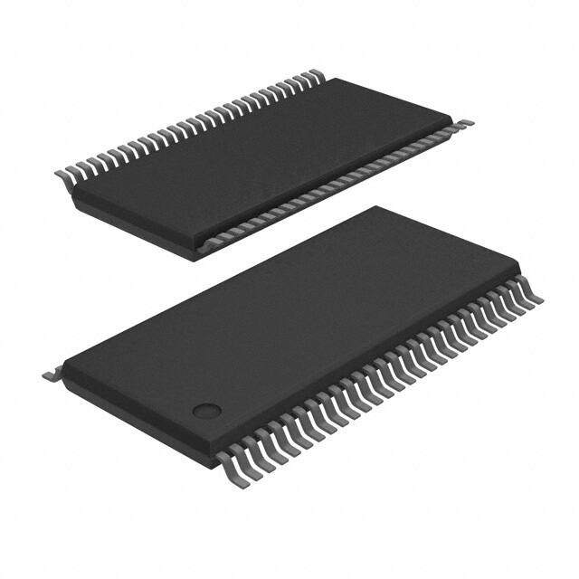
SN54LVT16543 . . . WD PACKAGE
SN74LVT16543 . . . DGG OR DL PACKAGE
(TOP VIEW)
Technology (ABT) Design for 3.3-V
Operation and Low-Static Power
Dissipation
Members of the Texas Instruments
Widebus Family
Support Mixed-Mode Signal Operation (5-V
Input and Output Voltages With 3.3-V VCC )
Support Unregulated Battery Operation
Down to 2.7 V
Typical VOLP (Output Ground Bounce)
< 0.8 V at VCC = 3.3 V, TA = 25°C
ESD Protection Exceeds 2000 V Per
MIL-STD-883C, Method 3015; Exceeds
200 V Using Machine Model
(C = 200 pF, R = 0)
Latch-Up Performance Exceeds 500 mA
Per JEDEC Standard JESD-17
Bus-Hold Data Inputs Eliminate the Need
for External Pullup Resistors
Support Live Insertion
Distributed VCC and GND Pin Configuration
Minimizes High-Speed Switching Noise
Flow-Through Architecture Optimizes
PCB Layout
Package Options Include Plastic 300-mil
Shrink Small-Outline (DL) and Thin Shrink
Small-Outline (DGG) Packages and 380-mil
Fine-Pitch Ceramic Flat (WD) Package
Using 25-mil Center-to-Center Spacings
1OEAB
1LEAB
1CEAB
GND
1A1
1A2
VCC
1A3
1A4
1A5
GND
1A6
1A7
1A8
2A1
2A2
2A3
GND
2A4
2A5
2A6
VCC
2A7
2A8
GND
2CEAB
2LEAB
2OEAB
1
56
2
55
3
54
4
53
5
52
6
51
7
50
8
49
9
48
10
47
11
46
12
45
13
44
14
43
15
42
16
41
17
40
18
39
19
38
20
37
21
36
22
35
23
34
24
33
25
32
26
31
27
30
28
29
1OEBA
1LEBA
1CEBA
GND
1B1
1B2
VCC
1B3
1B4
1B5
GND
1B6
1B7
1B8
2B1
2B2
2B3
GND
2B4
2B5
2B6
VCC
2B7
2B8
GND
2CEBA
2LEBA
2OEBA
description
The ’LVT16543 are 16-bit registered transceivers designed for low-voltage (3.3-V) VCC operation, but with the
capability to provide a TTL interface to a 5-V system environment. These devices can be used as two 8-bit
transceivers or one 16-bit transceiver. Separate latch-enable (LEAB or LEBA) and output-enable (OEAB or
OEBA) inputs are provided for each register to permit independent control in either direction of data flow.
The A-to-B enable (CEAB) input must be low in order to enter data from A or to output data from B. If CEAB
is low and LEAB is low, the A-to-B latches are transparent; a subsequent low-to-high transition of LEAB puts
the A latches in the storage mode. With CEAB and OEAB both low, the 3-state B outputs are active and reflect
the data present at the output of the A latches. Data flow from B to A is similar but requires using the CEBA,
LEBA, and OEBA inputs.
Active bus-hold circuitry is provided to hold unused or floating data inputs at a valid logic level.
Please be aware that an important notice concerning availability, standard warranty, and use in critical applications of
Texas Instruments semiconductor products and disclaimers thereto appears at the end of this data sheet.
Widebus is a trademark of Texas Instruments Incorporated.
Copyright 1995, Texas Instruments Incorporated
������ ��������� ����� ���� !"#$%&'� #"'�(�'� ����������
���� �')"*%(��"' #$**&'� (� ") +$,-�#(��"' !(�&
�*"!$#�� #"')"*% �"
�+&#�)�#(��"'� +&* ��& �&*%� ") �&.(� �'��*$%&'�� ��('!(*! /(**('�0
�*"!$#��"' +*"#&���'1 !"&� '"� '&#&��(*�-0 �'#-$!& �&���'1 ") (-+(*(%&�&*�
•
POST OFFICE BOX 655303 DALLAS, TEXAS 75265
POST OFFICE BOX 1443 HOUSTON, TEXAS 77251−1443
•
1
��������� ��
� �������� ��
�� ��� � ���� ���������� ������������
����
������ �������
SCBS148C − MAY 1992 − REVISED JULY 1995
description (continued)
To ensure the high-impedance state during power up or power down, OE should be tied to VCC through a pullup
resistor; the minimum value of the resistor is determined by the current-sinking capability of the driver.
The SN74LVT16543 is available in TI’s shrink small-outline (DL) and thin shrink small-outline (DGG) packages,
which provide twice the I/O pin count and functionality of standard small-outline packages in the same
printed-circuit-board area.
The SN54LVT16543 is characterized for operation over the full military temperature range of −55°C to 125°C.
The SN74LVT16543 is characterized for operation from − 40°C to 85°C.
logic symbol†
1OEBA
1CEBA
1LEBA
1OEAB
1CEAB
1LEAB
2OEBA
2CEBA
2LEBA
2OEAB
2CEAB
56
54
55
1
3
2
29
31
30
28
26
27
2LEAB
1A1
1EN3
G1
1C5
2EN4
G2
2C6
7EN9
G7
7C11
8EN10
G8
8C12
5
5D
3
6D
1A2
1A3
1A4
1A5
1A6
1A7
1A8
2A1
4
6
2A3
2A4
2A5
2A6
2A7
2A8
49
9
48
10
47
12
45
13
44
14
43
15
42
11D
9
16
10
41
17
40
19
38
20
37
21
36
23
34
24
33
† This symbol is in accordance with ANSI/IEEE Std 91-1984 and IEC Publication 617-12.
2
51
8
12D
2A2
52
•
POST OFFICE BOX 655303 DALLAS, TEXAS 75265
POST OFFICE BOX 1443 HOUSTON, TEXAS 77251−1443
•
1B1
1B2
1B3
1B4
1B5
1B6
1B7
1B8
2B1
2B2
2B3
2B4
2B5
2B6
2B7
2B8
��������� ��
� �������� ��
�� ��� � ���� ���������� ������������
����
������ �������
SCBS148C − MAY 1992 − REVISED JULY 1995
logic diagram (positive logic)
1OEBA
1CEBA
1LEBA
1OEAB
1CEAB
1LEAB
1A1
56
54
55
1
3
2
C1
5
1D
52
1B1
C1
1D
To Seven Other Channels
2OEBA
2CEBA
2LEBA
2OEAB
2CEAB
2LEAB
2A1
29
31
30
28
26
27
C1
15
1D
42
2B1
C1
1D
To Seven Other Channels
•
POST OFFICE BOX 655303 DALLAS, TEXAS 75265
POST OFFICE BOX 1443 HOUSTON, TEXAS 77251−1443
•
3
��������� ��
� �������� ��
�� ��� � ���� ���������� ������������
����
������ �������
SCBS148C − MAY 1992 − REVISED JULY 1995
FUNCTION TABLE†
(each 8-bit section)
INPUTS
CEAB
LEAB
OEAB
A
OUTPUT
B
H
X
X
X
Z
X
X
H
X
Z
L
H
L
X
L
L
L
L
B0‡
L
L
L
L
H
H
† A-to-B data flow is shown; B-to-A flow control is the
same except that it uses CEBA, LEBA, and OEBA.
‡ Output level before the indicated steady-state input
conditions were established
absolute maximum ratings over operating free-air temperature range (unless otherwise noted)§
Supply voltage range, VCC . . . . . . . . . . . . . . . . . . . . . . . . . . . . . . . . . . . . . . . . . . . . . . . . . . . . . . . . −0.5 V to 4.6 V
Input voltage range, VI (see Note 1) . . . . . . . . . . . . . . . . . . . . . . . . . . . . . . . . . . . . . . . . . . . . . . . . . . −0.5 V to 7 V
Voltage range applied to any output in the high state or power-off state, VO (see Note 1) . . . . −0.5 V to 7 V
Current into any output in the low state, IO: SN54LVT16543 . . . . . . . . . . . . . . . . . . . . . . . . . . . . . . . . . . . 96 mA
SN74LVT16543 . . . . . . . . . . . . . . . . . . . . . . . . . . . . . . . . . . 128 mA
Current into any output in the high state, IO (see Note 2): SN54LVT16543 . . . . . . . . . . . . . . . . . . . . . . . 48 mA
SN74LVT16543 . . . . . . . . . . . . . . . . . . . . . . . 64 mA
Input clamp current, IIK (VI < 0) . . . . . . . . . . . . . . . . . . . . . . . . . . . . . . . . . . . . . . . . . . . . . . . . . . . . . . . . . . −50 mA
Output clamp current, IOK (VO < 0) . . . . . . . . . . . . . . . . . . . . . . . . . . . . . . . . . . . . . . . . . . . . . . . . . . . . . . . −50 mA
Maximum power dissipation at TA = 55°C (in still air) (see Note 3): DGG package . . . . . . . . . . . . . . . . . . . 1 W
DL package . . . . . . . . . . . . . . . . . . . . 1.4 W
Storage temperature range, Tstg . . . . . . . . . . . . . . . . . . . . . . . . . . . . . . . . . . . . . . . . . . . . . . . . . . −65°C to 150°C
§ Stresses beyond those listed under “absolute maximum ratings” may cause permanent damage to the device. These are stress ratings only, and
functional operation of the device at these or any other conditions beyond those indicated under “recommended operating conditions” is not
implied. Exposure to absolute-maximum-rated conditions for extended periods may affect device reliability.
NOTES: 1. The input and output negative-voltage ratings may be exceeded if the input and output clamp-current ratings are observed.
2. This current flows only when the output is in the high state and VO > VCC.
3. The maximum package power dissipation is calculated using a junction temperature of 150°C and a board trace length of 750 mils.
For more information, refer to the Package Thermal Considerations application note in the 1994 ABT Advanced BiCMOS Technology
Data Book, literature number SCBD002B.
recommended operating conditions (see Note 4)
SN54LVT16543
SN74LVT16543
MIN
MAX
MIN
MAX
2.7
3.6
2.7
3.6
UNIT
VCC
VIH
Supply voltage
VIL
VI
Low-level input voltage
Input voltage
5.5
5.5
V
IOH
IOL
High-level output current
−24
−32
mA
Low-level output current
48
64
mA
∆t /∆v
Input transition rise or fall rate
10
ns / V
85
°C
High-level input voltage
2
Outputs enabled
TA
Operating free-air temperature
NOTE 4: Unused control inputs must be held high or low to prevent them from floating.
������� ������� �')"*%(��"' #"'#&*'� +*"!$#�� �' ��& )"*%(��2& "*
!&��1' +�(�& ") !&2&-"+%&'�
��(*(#�&*����# !(�( ('! "��&*
�+&#�)�#(��"'� (*& !&��1' 1"(-�
�&.(� �'��*$%&'�� *&�&*2&� ��& *�1�� �"
#�('1& "* !��#"'��'$& ��&�& +*"!$#�� /���"$� '"��#&
4
2
0.8
•
POST OFFICE BOX 655303 DALLAS, TEXAS 75265
POST OFFICE BOX 1443 HOUSTON, TEXAS 77251−1443
•
125
V
0.8
10
−55
−40
V
V
��������� ��
� �������� ��
�� ��� � ���� ���������� ������������
����
������ �������
SCBS148C − MAY 1992 − REVISED JULY 1995
electrical characteristics over recommended operating free-air temperature range (unless
otherwise noted)
PARAMETER
VIK
VOH
SN54LVT16543
TYP†
MAX
TEST CONDITIONS
VCC = 2.7 V,
VCC = MIN to MAX‡,
II = −18 mA
IOH = −100 µA
VCC = 2.7 V,
IOH = − 8 mA
IOH = − 24 mA
VCC = 3 V
VCC = 2.7 V
VOL
VCC = 3 V
VCC = 3.6 V,
VCC = 0 or MAX‡,
II
MIN
−1.2
VCC −0.2
2.4
2
0.2
0.2
IOL = 24 mA
IOL = 16 mA
0.5
0.5
0.4
0.4
IOL = 32 mA
IOL = 48 mA
0.5
0.5
IOL = 64 mA
VI = VCC or GND
VI = 5.5 V
VI = 5.5 V
V
0.55
0.55
Control inputs
A or B ports§
Ioff
VCC = 0,
II(hold)
VCC = 3 V
IOZH
IOZL
VCC = 3.6 V,
VCC = 3.6 V,
VI or VO = 0 to 4.5 V
VI = 0.8 V
A or B ports
VI = 2 V
VO = 3 V
±1
±1
10
10
20
20
5
5
−10
75
75
−75
−75
Outputs high
Outputs low
Outputs disabled
∆ICC¶
VCC = 3 V to 3.6 V,
One input at VCC − 0.6 V,
Other inputs at VCC or GND
Ci
VI = 3 V or 0
VO = 3 V or 0
4
µA
−10
± 100
VO = 0.5 V
IO = 0,
V
V
IOH = − 32 mA
IOL = 100 µA
VI = VCC
VI = 0
VCC = 3.6 V,
VI = VCC or GND
−1.2
UNIT
VCC −0.2
2.4
2
VCC = 3.6 V
ICC
SN74LVT16543
TYP†
MAX
MIN
µA
A
µA
1
1
µA
−1
−1
µA
0.12
0.12
5
5
0.12
0.12
0.2
0.2
mA
mA
4
pF
Cio
13
13
† All typical values are at VCC = 3.3 V, TA = 25°C.
‡ For conditions shown as MIN or MAX, use the appropriate value specified under recommended operating conditions.
§ Unused pins at VCC or GND
¶ This is the increase in supply current for each input that is at the specified TTL voltage level rather than VCC or GND.
pF
������� ������� �')"*%(��"' #"'#&*'� +*"!$#�� �' ��& )"*%(��2& "*
!&��1' +�(�& ") !&2&-"+%&'�
��(*(#�&*����# !(�( ('! "��&*
�+&#�)�#(��"'� (*& !&��1' 1"(-�
�&.(� �'��*$%&'�� *&�&*2&� ��& *�1�� �"
#�('1& "* !��#"'��'$& ��&�& +*"!$#�� /���"$� '"��#&
•
POST OFFICE BOX 655303 DALLAS, TEXAS 75265
POST OFFICE BOX 1443 HOUSTON, TEXAS 77251−1443
•
5
��������� ��
� �������� ��
�� ��� � ���� ���������� ������������
����
������ �������
SCBS148C − MAY 1992 − REVISED JULY 1995
timing requirements over recommended operating free-air temperature range (unless otherwise
noted) (see Figure 1)
SN54LVT16543
VCC = 3.3 V
± 0.3 V
MIN
tw
tsu
th
Pulse duration, LEAB or LEBA low
MAX
SN74LVT16543
VCC = 2.7 V
MIN
MAX
VCC = 3.3 V
± 0.3 V
MIN
MAX
VCC = 2.7 V
MIN
3.3
3.3
3.3
3.3
A or B before LEAB↑ or
LEBA↑
Data high
0.8
0.5
0.8
0.5
Data low
1.5
1.9
1.5
1.9
A or B before CEAB↑ or
CEBA↑
Data high
0.7
0.4
0.7
0.4
Data low
1.6
1.9
1.6
1.9
A or B after LEAB↑ or
LEBA↑
Data high
0.8
0
0.8
0
Data low
1.2
1.3
1.2
1.3
A or B after CEAB↑ or
CEBA↑
Data high
0.8
0
0.8
0
Data low
1.3
1.4
1.3
1.4
Setup time
Hold time
UNIT
MAX
ns
ns
ns
ns
ns
switching characteristics over recommended operating free-air temperature range, CL = 50 pF
(unless otherwise noted) (see Figure 1)
SN54LVT16543
PARAMETER
FROM
(INPUT)
TO
(OUTPUT)
tPLH
tPHL
A or B
B or A
tPLH
tPHL
LE
A or B
tPZH
tPZL
OE
A or B
tPHZ
tPLZ
OE
A or B
tPZH
tPZL
CE
A or B
tPHZ
tPLZ
CE
A or B
VCC = 3.3 V
± 0.3 V
SN74LVT16543
VCC = 2.7 V
MIN
MAX
VCC = 3.3 V
± 0.3 V
MIN TYP†
MAX
MIN
MAX
1.4
5
5.8
1.4
2.7
4.6
5.5
1.3
4.7
5.9
1.3
2.9
4.6
5.8
1.3
6.8
8.5
1.7
3.7
6.3
8.1
1.5
6.5
8.3
1.9
3.7
6
7.8
1.4
6
7.7
1.5
3.3
5.8
7.6
1.6
6.3
8.4
1.6
3.3
6.2
8.2
MIN
2
6.7
7.3
2
4.1
6.5
7.1
6
6.2
2.7
3.9
5.8
5.9
1.4
6.2
7.7
1.5
3.3
6
7.6
1.6
6.6
8.5
1.7
3.3
6.4
8.3
2
6.6
7.2
2
4.1
6.4
7.1
2.6
5.6
5.9
2.6
4
5.4
5.6
������� ������� �')"*%(��"' #"'#&*'� +*"!$#�� �' ��& )"*%(��2& "*
!&��1' +�(�& ") !&2&-"+%&'�
��(*(#�&*����# !(�( ('! "��&*
�+&#�)�#(��"'� (*& !&��1' 1"(-�
�&.(� �'��*$%&'�� *&�&*2&� ��& *�1�� �"
#�('1& "* !��#"'��'$& ��&�& +*"!$#�� /���"$� '"��#&
•
POST OFFICE BOX 655303 DALLAS, TEXAS 75265
POST OFFICE BOX 1443 HOUSTON, TEXAS 77251−1443
•
UNIT
MAX
2.7
† All typical values are at VCC = 3.3 V, TA = 25°C.
6
VCC = 2.7 V
ns
ns
ns
ns
ns
ns
��������� ��
� �������� ��
�� ��� � ���� ���������� ������������
����
������ �������
SCBS148C − MAY 1992 − REVISED JULY 1995
PARAMETER MEASUREMENT INFORMATION
6V
S1
500 Ω
From Output
Under Test
Open
GND
CL = 50 pF
(see Note A)
500 Ω
TEST
S1
tPLH/tPHL
tPLZ/tPZL
tPHZ/tPZH
Open
6V
GND
2.7 V
LOAD CIRCUIT FOR OUTPUTS
1.5 V
Timing Input
0V
tw
tsu
2.7 V
Input
1.5 V
th
2.7 V
1.5 V
1.5 V
Data Input
1.5 V
0V
0V
VOLTAGE WAVEFORMS
PULSE DURATION
VOLTAGE WAVEFORMS
SETUP AND HOLD TIMES
2.7 V
1.5 V
Input
0V
1.5 V
1.5 V
VOL
tPLH
tPHL
Output
Waveform 2
S1 at GND
(see Note B)
VOH
Output
1.5 V
1.5 V
0V
tPLZ
Output
Waveform 1
S1 at 6 V
(see Note B)
VOH
Output
1.5 V
tPZL
tPHL
tPLH
2.7 V
Output
Control
1.5 V
1.5 V
VOL
VOLTAGE WAVEFORMS
PROPAGATION DELAY TIMES
INVERTING AND NONINVERTING OUTPUTS
1.5 V
tPZH
3V
VOL + 0.3 V
VOL
tPHZ
1.5 V
VOH − 0.3 V
VOH
[0V
VOLTAGE WAVEFORMS
ENABLE AND DISABLE TIMES
LOW- AND HIGH-LEVEL ENABLING
NOTES: A. CL includes probe and jig capacitance.
B. Waveform 1 is for an output with internal conditions such that the output is low except when disabled by the output control.
Waveform 2 is for an output with internal conditions such that the output is high except when disabled by the output control.
C. All input pulses are supplied by generators having the following characteristics: PRR ≤ 10 MHz, ZO = 50 Ω, tr ≤ 2.5 ns, tf ≤ 2.5 ns.
D. The outputs are measured one at a time with one transition per measurement.
Figure 1. Load Circuit and Voltage Waveforms
•
POST OFFICE BOX 655303 DALLAS, TEXAS 75265
POST OFFICE BOX 1443 HOUSTON, TEXAS 77251−1443
•
7
�PACKAGE MATERIALS INFORMATION
www.ti.com
5-Jan-2022
TAPE AND REEL INFORMATION
*All dimensions are nominal
Device
Package Package Pins
Type Drawing
SPQ
Reel
Reel
A0
Diameter Width (mm)
(mm) W1 (mm)
B0
(mm)
K0
(mm)
P1
(mm)
W
Pin1
(mm) Quadrant
SN74LVT16543DGGR
TSSOP
DGG
56
2000
330.0
24.4
8.6
15.6
1.8
12.0
24.0
Q1
SN74LVT16543DLR
SSOP
DL
56
1000
330.0
32.4
11.35
18.67
3.1
16.0
32.0
Q1
Pack Materials-Page 1
�PACKAGE MATERIALS INFORMATION
www.ti.com
5-Jan-2022
*All dimensions are nominal
Device
Package Type
Package Drawing
Pins
SPQ
Length (mm)
Width (mm)
Height (mm)
SN74LVT16543DGGR
TSSOP
DGG
56
2000
367.0
367.0
45.0
SN74LVT16543DLR
SSOP
DL
56
1000
367.0
367.0
55.0
Pack Materials-Page 2
�PACKAGE MATERIALS INFORMATION
www.ti.com
5-Jan-2022
TUBE
*All dimensions are nominal
Device
Package Name
Package Type
Pins
SPQ
L (mm)
W (mm)
T (µm)
B (mm)
SN74LVT16543DL
DL
SSOP
56
20
473.7
14.24
5110
7.87
Pack Materials-Page 3
��PACKAGE OUTLINE
DGG0056A
TSSOP - 1.2 mm max height
SCALE 1.200
SMALL OUTLINE PACKAGE
C
8.3
TYP
7.9
SEATING PLANE
PIN 1 ID
AREA
A
0.1 C
54X 0.5
56
1
14.1
13.9
NOTE 3
2X
13.5
28
B
6.2
6.0
29
56X
0.27
0.17
0.08
1.2 MAX
C A
B
(0.15) TYP
SEE DETAIL A
0.25
GAGE PLANE
0 -8
0.15
0.05
0.75
0.50
DETAIL A
TYPICAL
4222167/A 07/2015
NOTES:
1. All linear dimensions are in millimeters. Any dimensions in parenthesis are for reference only. Dimensioning and tolerancing
per ASME Y14.5M.
2. This drawing is subject to change without notice.
3. This dimension does not include mold flash, protrusions, or gate burrs. Mold flash, protrusions, or gate burrs shall not
exceed 0.15 mm per side.
4. Reference JEDEC registration MO-153.
www.ti.com
�EXAMPLE BOARD LAYOUT
DGG0056A
TSSOP - 1.2 mm max height
SMALL OUTLINE PACKAGE
56X (1.5)
SYMM
1
56
56X (0.3)
54X (0.5)
(R0.05)
TYP
SYMM
28
29
(7.5)
LAND PATTERN EXAMPLE
SCALE:6X
SOLDER MASK
OPENING
METAL
SOLDER MASK
OPENING
METAL UNDER
SOLDER MASK
0.05 MAX
ALL AROUND
0.05 MIN
ALL AROUND
SOLDER MASK
DEFINED
NON SOLDER MASK
DEFINED
SOLDER MASK DETAILS
4222167/A 07/2015
NOTES: (continued)
5. Publication IPC-7351 may have alternate designs.
6. Solder mask tolerances between and around signal pads can vary based on board fabrication site.
www.ti.com
�EXAMPLE STENCIL DESIGN
DGG0056A
TSSOP - 1.2 mm max height
SMALL OUTLINE PACKAGE
56X (1.5)
SYMM
1
56
56X (0.3)
54X (0.5)
(R0.05) TYP
SYMM
29
28
(7.5)
SOLDER PASTE EXAMPLE
BASED ON 0.125 mm THICK STENCIL
SCALE:6X
4222167/A 07/2015
NOTES: (continued)
7. Laser cutting apertures with trapezoidal walls and rounded corners may offer better paste release. IPC-7525 may have alternate
design recommendations.
8. Board assembly site may have different recommendations for stencil design.
www.ti.com
�IMPORTANT NOTICE AND DISCLAIMER
TI PROVIDES TECHNICAL AND RELIABILITY DATA (INCLUDING DATA SHEETS), DESIGN RESOURCES (INCLUDING REFERENCE
DESIGNS), APPLICATION OR OTHER DESIGN ADVICE, WEB TOOLS, SAFETY INFORMATION, AND OTHER RESOURCES “AS IS”
AND WITH ALL FAULTS, AND DISCLAIMS ALL WARRANTIES, EXPRESS AND IMPLIED, INCLUDING WITHOUT LIMITATION ANY
IMPLIED WARRANTIES OF MERCHANTABILITY, FITNESS FOR A PARTICULAR PURPOSE OR NON-INFRINGEMENT OF THIRD
PARTY INTELLECTUAL PROPERTY RIGHTS.
These resources are intended for skilled developers designing with TI products. You are solely responsible for (1) selecting the appropriate
TI products for your application, (2) designing, validating and testing your application, and (3) ensuring your application meets applicable
standards, and any other safety, security, regulatory or other requirements.
These resources are subject to change without notice. TI grants you permission to use these resources only for development of an
application that uses the TI products described in the resource. Other reproduction and display of these resources is prohibited. No license
is granted to any other TI intellectual property right or to any third party intellectual property right. TI disclaims responsibility for, and you
will fully indemnify TI and its representatives against, any claims, damages, costs, losses, and liabilities arising out of your use of these
resources.
TI’s products are provided subject to TI’s Terms of Sale or other applicable terms available either on ti.com or provided in conjunction with
such TI products. TI’s provision of these resources does not expand or otherwise alter TI’s applicable warranties or warranty disclaimers for
TI products.
TI objects to and rejects any additional or different terms you may have proposed. IMPORTANT NOTICE
Mailing Address: Texas Instruments, Post Office Box 655303, Dallas, Texas 75265
Copyright © 2022, Texas Instruments Incorporated
�


 工商网监
湘ICP备2023018690号
工商网监
湘ICP备2023018690号
