SN54LVTH18504A, SN54LVTH182504A, SN74LVTH18504A, SN74LVTH182504A
3.3-V ABT SCAN TEST DEVICES
WITH 20-BIT UNIVERSAL BUS TRANSCEIVERS
SCBS667B – JULY 1996 – REVISED JUNE 1997
D
D
D
D
D
D
D
Members of the Texas Instruments
SCOPE Family of Testability Products
Members of the Texas Instruments
Widebus Family
State-of-the-Art 3.3-V ABT Design Supports
Mixed-Mode Signal Operation (5-V Input
and Output Voltages With 3.3-V VCC)
Support Unregulated Battery Operation
Down to 2.7 V
UBT (Universal Bus Transceiver)
Combines D-Type Latches and D-Type
Flip-Flops for Operation in Transparent,
Latched, or Clocked Mode
Bus Hold on Data Inputs Eliminates the
Need for External Pullup/Pulldown
Resistors
B-Port Outputs of ’LVTH182504A Devices
Have Equivalent 25-Ω Series Resistors, So
No External Resistors Are Required
D
D
D
Compatible With the IEEE Std 1149.1-1990
(JTAG) Test Access Port and
Boundary-Scan Architecture
SCOPE Instruction Set
– IEEE Std 1149.1-1990 Required
Instructions and Optional CLAMP and
HIGHZ
– Parallel-Signature Analysis at Inputs
– Pseudo-Random Pattern Generation
From Outputs
– Sample Inputs/Toggle Outputs
– Binary Count From Outputs
– Device Identification
– Even-Parity Opcodes
Packaged in 64-Pin Plastic Thin Quad Flat
(PM) Packages Using 0.5-mm
Center-to-Center Spacings and 68-Pin
Ceramic Quad Flat (HV) Packages Using
25-mil Center-to-Center Spacings
description
The ’LVTH18504A and ’LVTH182504A scan test devices with 20-bit universal bus transceivers are members
of the Texas Instruments (TI) SCOPE testability integrated-circuit family. This family of devices supports
IEEE Std 1149.1-1990 boundary scan to facilitate testing of complex circuit-board assemblies. Scan access to
the test circuitry is accomplished via the 4-wire test access port (TAP) interface.
Additionally, these devices are designed specifically for low-voltage (3.3-V) VCC operation, but with the
capability to provide a TTL interface to a 5-V system environment.
In the normal mode, these devices are 20-bit universal bus transceivers that combine D-type latches and D-type
flip-flops to allow data flow in transparent, latched, or clocked modes. The test circuitry can be activated by the
TAP to take snapshot samples of the data appearing at the device pins or to perform a self-test on the
boundary-test cells. Activating the TAP in the normal mode does not affect the functional operation of the
SCOPE universal bus transceivers.
Data flow in each direction is controlled by output-enable (OEAB and OEBA), latch-enable (LEAB and LEBA),
clock-enable (CLKENAB and CLKENBA), and clock (CLKAB and CLKBA) inputs. For A-to-B data flow, the
device operates in the transparent mode when LEAB is high. When LEAB is low, the A-bus data is latched while
CLKENAB is high and/or CLKAB is held at a static low or high logic level. Otherwise, if LEAB is low and
CLKENAB is low, A-bus data is stored on a low-to-high transition of CLKAB. When OEAB is low, the B outputs
are active. When OEAB is high, the B outputs are in the high-impedance state. B-to-A data flow is similar to
A-to-B data flow, but uses the OEBA, LEBA, CLKENBA, and CLKBA inputs.
In the test mode, the normal operation of the SCOPE universal bus transceivers is inhibited, and the test circuitry
is enabled to observe and control the I/O boundary of the device. When enabled, the test circuitry performs
boundary-scan test operations according to the protocol described in IEEE Std 1149.1-1990.
Please be aware that an important notice concerning availability, standard warranty, and use in critical applications of
Texas Instruments semiconductor products and disclaimers thereto appears at the end of this data sheet.
SCOPE, UBT, and Widebus are trademarks of Texas Instruments Incorporated.
Copyright 1997, Texas Instruments Incorporated
UNLESS OTHERWISE NOTED this document contains PRODUCTION
DATA information current as of publication date. Products conform to
specifications per the terms of Texas Instruments standard warranty.
Production processing does not necessarily include testing of all
parameters.
POST OFFICE BOX 655303
• DALLAS, TEXAS 75265
1
�SN54LVTH18504A, SN54LVTH182504A, SN74LVTH18504A, SN74LVTH182504A
3.3-V ABT SCAN TEST DEVICES
WITH 20-BIT UNIVERSAL BUS TRANSCEIVERS
SCBS667B – JULY 1996 – REVISED JUNE 1997
description (continued)
Four dedicated test pins are used to observe and control the operation of the test circuitry: test data input (TDI),
test data output (TDO), test mode select (TMS), and test clock (TCK). Additionally, the test circuitry performs
other testing functions, such as parallel-signature analysis (PSA) on data inputs and pseudo-random pattern
generation (PRPG) from data outputs. All testing and scan operations are synchronized to the TAP interface.
Active bus-hold circuitry is provided to hold unused or floating data inputs at a valid logic level.
The B-port outputs of ’LVTH182504A, which are designed to source or sink up to 12 mA, include equivalent 25-Ω
series resistors to reduce overshoot and undershoot.
The SN54LVTH18504A and SN54LVTH182504A are characterized for operation over the full military
temperature range of –55°C to 125°C. The SN74LVTH18504A and SN74LVTH182504A are characterized for
operation from –40°C to 85°C.
A4
A5
A6
GND
A7
A8
A9
A10
NC
VCC
A11
A12
A13
GND
A14
A15
A16
A3
A2
A1
GND
OEBA
LEBA
TDO
VCC
NC
TMS
CLKBA
CLKENBA
B1
GND
B2
B3
B4
SN54LVTH18504A, SN54LVTH182504A . . . HV PACKAGE
(TOP VIEW)
9
5 4 3
8 7
6
2 1 68 67 66 65 64 63 62 61
10
60
11
59
12
58
13
57
14
56
15
55
16
54
17
53
18
52
19
51
20
50
21
49
22
48
23
47
24
46
25
45
26
44
TCK
LEAB
OEAB
GND
B20
B19
B18
VCC
A17
A18
A19
GND
A20
CLKENAB
CLKAB
TDI
NC
27 28 29 30 31 32 33 34 35 36 37 38 39 40 41 42 43
NC – No internal connection
2
POST OFFICE BOX 655303
• DALLAS, TEXAS 75265
B5
B6
B7
GND
B8
B9
B10
VCC
NC
B11
B12
B13
B14
GND
B15
B16
B17
�SN54LVTH18504A, SN54LVTH182504A, SN74LVTH18504A, SN74LVTH182504A
3.3-V ABT SCAN TEST DEVICES
WITH 20-BIT UNIVERSAL BUS TRANSCEIVERS
SCBS667B – JULY 1996 – REVISED JUNE 1997
A3
A2
A1
GND
OEBA
LEBA
TDO
V CC
TMS
CLKBA
CLKENBA
B1
GND
B2
B3
B4
SN74LVTH18504A, SN74LVTH182504A . . . PM PACKAGE
(TOP VIEW)
64 63 62 61 60 59 58 57 56 55 54 53 52 51 50 49
1
48
2
47
3
46
4
45
5
44
6
43
7
42
8
41
9
40
10
39
11
38
12
37
13
36
14
35
15
34
16
33
B5
B6
B7
GND
B8
B9
B10
VCC
B11
B12
B13
B14
GND
B15
B16
B17
17 18 19 20 21 22 23 24 25 26 27 28 29 30 31 32
A17
A18
A19
GND
A20
CLKENAB
CLKAB
TDI
VCC
TCK
LEAB
OEAB
GND
B20
B19
B18
A4
A5
A6
GND
A7
A8
A9
A10
VCC
A11
A12
A13
GND
A14
A15
A16
FUNCTION TABLE†
(normal mode, each register)
INPUTS
OUTPUT
B
OEAB
LEAB
CLKENAB
CLKAB
A
L
L
L
L
X
L
L
L
↑
L
L
L
L
↑
H
H
L
L
H
X
X
L
H
X
X
L
B0‡
L
L
H
X
X
H
H
B0‡
L
H
X
X
X
X
Z
† A-to-B data flow is shown. B-to-A data flow is similar, but uses
OEBA, LEBA, CLKENBA, and CLKBA.
‡ Output level before the indicated steady-state input conditions were
established
POST OFFICE BOX 655303
• DALLAS, TEXAS 75265
3
�SN54LVTH18504A, SN54LVTH182504A, SN74LVTH18504A, SN74LVTH182504A
3.3-V ABT SCAN TEST DEVICES
WITH 20-BIT UNIVERSAL BUS TRANSCEIVERS
SCBS667B – JULY 1996 – REVISED JUNE 1997
functional block diagram
Boundary-Scan Register
CLKENAB
LEAB
CLKAB
OEAB
CLKENBA
LEBA
CLKBA
OEBA
A1
22
27
23
VCC
28
54
59
55
VCC
60
C1
C1
1D
1D
53
62
C1
1D
B1
C1
1D
1 of 20 Channels
Bypass Register
Boundary-Control
Register
Identification
Register
VCC
TDI
58
Instruction
Register
24
VCC
TMS
TCK
56
26
TAP
Controller
Pin numbers shown are for the PM package.
4
POST OFFICE BOX 655303
• DALLAS, TEXAS 75265
TDO
�SN54LVTH18504A, SN54LVTH182504A, SN74LVTH18504A, SN74LVTH182504A
3.3-V ABT SCAN TEST DEVICES
WITH 20-BIT UNIVERSAL BUS TRANSCEIVERS
SCBS667B – JULY 1996 – REVISED JUNE 1997
Terminal Functions
TERMINAL NAME
DESCRIPTION
A1–A20
Normal-function A-bus I/O ports. See function table for normal-mode logic.
B1–B20
Normal-function B-bus I/O ports. See function table for normal-mode logic.
CLKAB, CLKBA
CLKENAB, CLKENBA
GND
Normal-function clock inputs. See function table for normal-mode logic.
Normal-function clock enables. See function table for normal-mode logic.
Ground
LEAB, LEBA
Normal-function latch enables. See function table for normal-mode logic.
OEAB, OEBA
Normal-function output enables. See function table for normal-mode logic. An internal pullup at each terminal forces
the terminal to a high level if left unconnected.
TCK
Test clock. One of four terminals required by IEEE Std 1149.1-1990. Test operations of the device are synchronous
to TCK. Data is captured on the rising edge of TCK and outputs change on the falling edge of TCK.
TDI
Test data input. One of four terminals required by IEEE Std 1149.1-1990. TDI is the serial input for shifting data
through the instruction register or selected data register. An internal pullup forces TDI to a high level if left
unconnected.
TDO
Test data output. One of four terminals required by IEEE Std 1149.1-1990. TDO is the serial output for shifting data
through the instruction register or selected data register.
TMS
Test mode select. One of four terminals required by IEEE Std 1149.1-1990. TMS directs the device through its TAP
controller states. An internal pullup forces TMS to a high level if left unconnected.
VCC
Supply voltage
POST OFFICE BOX 655303
• DALLAS, TEXAS 75265
5
�SN54LVTH18504A, SN54LVTH182504A, SN74LVTH18504A, SN74LVTH182504A
3.3-V ABT SCAN TEST DEVICES
WITH 20-BIT UNIVERSAL BUS TRANSCEIVERS
SCBS667B – JULY 1996 – REVISED JUNE 1997
test architecture
Serial-test information is conveyed by means of a 4-wire test bus or TAP that conforms to IEEE Std 1149.1-1990.
Test instructions, test data, and test control signals are passed along this serial-test bus. The TAP controller
monitors two signals from the test bus: TCK and TMS. The TAP controller extracts the synchronization (TCK)
and state control (TMS) signals from the test bus and generates the appropriate on-chip control signals for the
test structures in the device. Figure 1 shows the TAP-controller state diagram.
The TAP controller is fully synchronous to the TCK signal. Input data is captured on the rising edge of TCK and
output data changes on the falling edge of TCK. This scheme ensures data to be captured is valid for fully
one-half of the TCK cycle.
The functional block diagram shows the IEEE Std 1149.1-1990 4-wire test bus and boundary-scan architecture
and the relationships of the test bus, the TAP controller, and the test registers. As shown, the device contains
an 8-bit instruction register and four test data registers: a 48-bit boundary-scan register, a 3-bit boundary-control
register, a 1-bit bypass register, and a 32-bit device-identification register.
Test-Logic-Reset
TMS = H
TMS = L
TMS = H
TMS = H
Run-Test/Idle
TMS = H
Select-DR-Scan
Select-IR-Scan
TMS = L
TMS = L
TMS = L
TMS = H
TMS = H
Capture-DR
Capture-IR
TMS = L
TMS = L
Shift-DR
Shift-IR
TMS = L
TMS = L
TMS = H
TMS = H
TMS = H
TMS = H
Exit1-DR
Exit1-IR
TMS = L
TMS = L
Pause-DR
Pause-IR
TMS = L
TMS = L
TMS = H
TMS = H
TMS = L
TMS = L
Exit2-DR
Exit2-IR
TMS = H
Update-DR
TMS = H
TMS = L
Figure 1. TAP-Controller State Diagram
6
POST OFFICE BOX 655303
• DALLAS, TEXAS 75265
TMS = H
Update-IR
TMS = H
TMS = L
�SN54LVTH18504A, SN54LVTH182504A, SN74LVTH18504A, SN74LVTH182504A
3.3-V ABT SCAN TEST DEVICES
WITH 20-BIT UNIVERSAL BUS TRANSCEIVERS
SCBS667B – JULY 1996 – REVISED JUNE 1997
state diagram description
The TAP controller is a synchronous finite-state machine that provides test control signals throughout the
device. The state diagram shown in Figure 1 is in accordance with IEEE Std 1149.1-1990. The TAP controller
proceeds through its states, based on the level of TMS at the rising edge of TCK.
As shown, the TAP controller consists of 16 states. There are six stable states (indicated by a looping arrow in
the state diagram) and ten unstable states. A stable state is defined as a state the TAP controller can retain for
consecutive TCK cycles. Any state that does not meet this criterion is an unstable state.
There are two main paths through the state diagram: one to access and control the selected data register and
one to access and control the instruction register. Only one register at a time can be accessed.
Test-Logic-Reset
The device powers up in the Test-Logic-Reset state. In the stable Test-Logic-Reset state, the test logic is reset
and is disabled so that the normal logic function of the device is performed. The instruction register is reset to
an opcode that selects the optional IDCODE instruction, if supported, or the BYPASS instruction. Certain data
registers also can be reset to their power-up values.
The state machine is constructed such that the TAP controller returns to the Test-Logic-Reset state in no more
than five TCK cycles if TMS is left high. The TMS pin has an internal pullup resistor that forces it high if left
unconnected or if a board defect causes it to be open circuited.
For the ’LVTH18504A and ’LVTH182504A, the instruction register is reset to the binary value 10000001, which
selects the IDCODE instruction. Bits 47–46 in the boundary-scan register are reset to logic 1, ensuring that
these cells, which control A-port and B-port outputs, are set to benign values (i.e., if test mode were invoked,
the outputs would be at high-impedance state). Reset values of other bits in the boundary-scan register should
be considered indeterminate. The boundary-control register is reset to the binary value 010, which selects the
PSA test operation.
Run-Test/Idle
The TAP controller must pass through the Run-Test/Idle state (from Test-Logic-Reset) before executing any test
operations. The Run-Test/Idle state also can be entered following data-register or instruction-register scans.
Run-Test/Idle is a stable state in which the test logic can be actively running a test or can be idle. The test
operations selected by the boundary-control register are performed while the TAP controller is in the
Run-Test/Idle state.
Select-DR-Scan, Select-lR-Scan
No specific function is performed in the Select-DR-Scan and Select-lR-Scan states, and the TAP controller exits
either of these states on the next TCK cycle. These states allow the selection of either data-register scan or
instruction-register scan.
Capture-DR
When a data-register scan is selected, the TAP controller must pass through the Capture-DR state. In the
Capture-DR state, the selected data register can capture a data value as specified by the current instruction.
Such capture operations occur on the rising edge of TCK, upon which the TAP controller exits the
Capture-DR state.
POST OFFICE BOX 655303
• DALLAS, TEXAS 75265
7
�SN54LVTH18504A, SN54LVTH182504A, SN74LVTH18504A, SN74LVTH182504A
3.3-V ABT SCAN TEST DEVICES
WITH 20-BIT UNIVERSAL BUS TRANSCEIVERS
SCBS667B – JULY 1996 – REVISED JUNE 1997
Shift-DR
Upon entry to the Shift-DR state, the data register is placed in the scan path between TDI and TDO. On the first
falling edge of TCK, TDO goes from the high-impedance state to an active state. TDO enables to the logic level
present in the least-significant bit of the selected data register.
While in the stable Shift-DR state, data is serially shifted through the selected data register on each TCK cycle.
The first shift occurs on the first rising edge of TCK after entry to the Shift-DR state (i.e., no shifting occurs during
the TCK cycle, in which the TAP controller changes from Capture-DR to Shift-DR or from Exit2-DR to Shift-DR).
The last shift occurs on the rising edge of TCK, upon which the TAP controller exits the Shift-DR state.
Exit1-DR, Exit2-DR
The Exit1-DR and Exit2-DR states are temporary states that end a data-register scan. It is possible to return
to the Shift-DR state from either Exit1-DR or Exit2-DR without recapturing the data register. On the first falling
edge of TCK after entry to Exit1-DR, TDO goes from the active state to the high-impedance state.
Pause-DR
No specific function is performed in the stable Pause-DR state, in which the TAP controller can remain
indefinitely. The Pause-DR state suspends and resumes data-register scan operations without loss of data.
Update-DR
If the current instruction calls for the selected data register to be updated with current data, such updates occur
on the falling edge of TCK, following entry to the Update-DR state.
Capture-IR
When an instruction-register scan is selected, the TAP controller must pass through the Capture-IR state. In
the Capture-IR state, the instruction register captures its current status value. This capture operation occurs
on the rising edge of TCK, upon which the TAP controller exits the Capture-IR state. For the ’LVTH18504A and
’LVTH182504A, the status value loaded in the Capture-IR state is the fixed binary value 10000001.
Shift-IR
Upon entry to the Shift-IR state, the instruction register is placed in the scan path between TDI and TDO. On
the first falling edge of TCK, TDO goes from the high-impedance state to the active state. TDO enables to the
logic level present in the least-significant bit of the instruction register.
While in the stable Shift-IR state, instruction data is serially shifted through the instruction register on each TCK
cycle. The first shift occurs on the first rising edge of TCK after entry to the Shift-IR state (i.e., no shifting occurs
during the TCK cycle in which the TAP controller changes from Capture-IR to Shift-IR or from Exit2-IR to
Shift-IR). The last shift occurs on the rising edge of TCK, upon which the TAP controller exits the Shift-IR state.
Exit1-IR, Exit2-IR
The Exit1-IR and Exit2-IR states are temporary states that end an instruction-register scan. It is possible to
return to the Shift-IR state from either Exit1-IR or Exit2-IR without recapturing the instruction register. On the
first falling edge of TCK after entry to Exit1-IR, TDO goes from the active state to the high-impedance state.
Pause-IR
No specific function is performed in the stable Pause-IR state, in which the TAP controller can remain
indefinitely. The Pause-IR state suspends and resumes instruction-register scan operations without loss
of data.
Update-IR
The current instruction is updated and takes effect on the falling edge of TCK, following entry to the
Update-IR state.
8
POST OFFICE BOX 655303
• DALLAS, TEXAS 75265
�SN54LVTH18504A, SN54LVTH182504A, SN74LVTH18504A, SN74LVTH182504A
3.3-V ABT SCAN TEST DEVICES
WITH 20-BIT UNIVERSAL BUS TRANSCEIVERS
SCBS667B – JULY 1996 – REVISED JUNE 1997
register overview
With the exception of the bypass and device-identification registers, any test register can be thought of as a
serial-shift register with a shadow latch on each bit. The bypass and device-identification registers differ in that
they contain only a shift register. During the appropriate capture state (Capture-IR for instruction register,
Capture-DR for data registers), the shift register can be parallel loaded from a source specified by the current
instruction. During the appropriate shift state (Shift-IR or Shift-DR), the contents of the shift register are shifted
out from TDO while new contents are shifted in at TDI. During the appropriate update state (Update-IR or
Update-DR), the shadow latches are updated from the shift register.
instruction register description
The instruction register (IR) is eight bits long and tells the device what instruction is to be executed. Information
contained in the instruction includes the mode of operation (either normal mode, in which the device performs
its normal logic function, or test mode, in which the normal logic function is inhibited or altered), the test operation
to be performed, which of the four data registers is to be selected for inclusion in the scan path during
data-register scans, and the source of data to be captured into the selected data register during Capture-DR.
Table 3 lists the instructions supported by the ’LVTH18504A and ’LVTH182504A. The even-parity feature
specified for SCOPE devices is supported in this device. Bit 7 of the instruction opcode is the parity bit. Any
instructions that are defined for SCOPE devices but are not supported by this device default to BYPASS.
During Capture-IR, the IR captures the binary value 10000001. As an instruction is shifted in, this value is shifted
out via TDO and can be inspected as verification that the IR is in the scan path. During Update-IR, the value
that has been shifted into the IR is loaded into shadow latches. At this time, the current instruction is updated
and any specified mode change takes effect. At power up or in the Test-Logic-Reset state, the IR is reset to the
binary value 10000001, which selects the IDCODE instruction. The instruction register order of scan is shown
in Figure 2.
TDI
Bit 7
Parity
(MSB)
Bit 6
Bit 5
Bit 4
Bit 3
Bit 2
Bit 1
Bit 0
(LSB)
TDO
Figure 2. Instruction Register Order of Scan
POST OFFICE BOX 655303
• DALLAS, TEXAS 75265
9
�SN54LVTH18504A, SN54LVTH182504A, SN74LVTH18504A, SN74LVTH182504A
3.3-V ABT SCAN TEST DEVICES
WITH 20-BIT UNIVERSAL BUS TRANSCEIVERS
SCBS667B – JULY 1996 – REVISED JUNE 1997
data register description
boundary-scan register
The boundary-scan register (BSR) is 48 bits long. It contains one boundary-scan cell (BSC) for each
normal-function input pin and one BSC for each normal-function I/O pin (one single cell for both input data and
output data). The BSR is used to store test data that is to be applied externally to the device output pins, and/or
to capture data that appears internally at the outputs of the normal on-chip logic and/or externally at the device
input pins.
The source of data to be captured into the BSR during Capture-DR is determined by the current instruction. The
contents of the BSR can change during Run-Test/Idle as determined by the current instruction. At power up or
in Test-Logic-Reset, BSCs 47–46 are reset to logic 1, ensuring that these cells, which control A-port and B-port
outputs, are set to benign values (i.e., if test mode were invoked, the outputs would be at high-impedance state).
Reset values of other BSCs should be considered indeterminate.
The BSR order of scan is from TDI through bits 47–0 to TDO. Table 1 shows the BSR bits and their associated
device pin signals.
Table 1. Boundary-Scan Register Configuration
10
BSR BIT
NUMBER
DEVICE
SIGNAL
BSR BIT
NUMBER
DEVICE
SIGNAL
BSR BIT
NUMBER
DEVICE
SIGNAL
47
OEAB
39
A20-I/O
19
B20-I/O
46
OEBA
38
A19-I/O
18
B19-I/O
45
CLKAB
37
A18-I/O
17
B18-I/O
44
CLKBA
36
A17-I/O
16
B17-I/O
43
CLKENAB
35
A16-I/O
15
B16-I/O
42
CLKENBA
34
A15-I/O
14
B15-I/O
41
LEAB
33
A14-I/O
13
B14-I/O
40
LEBA
32
A13-I/O
12
B13-I/O
––
––
31
A12-I/O
11
B12-I/O
––
––
30
A11-I/O
10
B11-I/O
––
––
29
A10-I/O
9
B10-I/O
––
––
28
A9-I/O
8
B9-I/O
––
––
27
A8-I/O
7
B8-I/O
––
––
26
A7-I/O
6
B7-I/O
––
––
25
A6-I/O
5
B6-I/O
––
––
24
A5-I/O
4
B5-I/O
––
––
23
A4-I/O
3
B4-I/O
––
––
22
A3-I/O
2
B3-I/O
––
––
21
A2-I/O
1
B2-I/O
––
––
20
A1-I/O
0
B1-I/O
POST OFFICE BOX 655303
• DALLAS, TEXAS 75265
�SN54LVTH18504A, SN54LVTH182504A, SN74LVTH18504A, SN74LVTH182504A
3.3-V ABT SCAN TEST DEVICES
WITH 20-BIT UNIVERSAL BUS TRANSCEIVERS
SCBS667B – JULY 1996 – REVISED JUNE 1997
boundary-control register
The boundary-control register (BCR) is three bits long. The BCR is used in the context of the boundary-run
(RUNT) instruction to implement additional test operations not included in the basic SCOPE instruction set.
Such operations include PRPG, PSA, and binary count up (COUNT). Table 4 shows the test operations that
are decoded by the BCR.
During Capture-DR, the contents of the BCR are not changed. At power up or in Test-Logic-Reset, the BCR is
reset to the binary value 010, which selects the PSA test operation. The boundary-control register order of scan
is shown in Figure 3.
TDI
Bit 2
(MSB)
Bit 1
Bit 0
(LSB)
TDO
Figure 3. Boundary-Control Register Order of Scan
bypass register
The bypass register is a 1-bit scan path that can be selected to shorten the length of the system scan path,
reducing the number of bits per test pattern that must be applied to complete a test operation. During
Capture-DR, the bypass register captures a logic 0. The bypass register order of scan is shown in Figure 4.
TDI
Bit 0
TDO
Figure 4. Bypass Register Order of Scan
POST OFFICE BOX 655303
• DALLAS, TEXAS 75265
11
�SN54LVTH18504A, SN54LVTH182504A, SN74LVTH18504A, SN74LVTH182504A
3.3-V ABT SCAN TEST DEVICES
WITH 20-BIT UNIVERSAL BUS TRANSCEIVERS
SCBS667B – JULY 1996 – REVISED JUNE 1997
device-identification register
The device-identification register (IDR) is 32 bits long. It can be selected and read to identify the manufacturer,
part number, and version of this device.
For the ’LVTH18504A, either of the binary values 00100000000000011101000000101111 (2001D02F, hex) or
00110000000000011101000000101111 (3001D02F, hex) is captured (during Capture-DR state) in the IDR to
identify this device as TI SN54/74LVTH18504A.
For the ’LVTH182504A, either of the binary values 00010000000000100010000000101111 (1002202F, hex)
or 00100000000000100010000000101111 (2002202F, hex) is captured (during Capture-DR state) in the IDR
to identify this device as TI SN54/74LVTH182504A.
The IDR order of scan is from TDI through bits 31–0 to TDO. Table 2 shows the IDR bits and their significance.
Table 2. Device-Identification Register Configuration
IDR BIT
NUMBER
IDENTIFICATION
SIGNIFICANCE
IDR BIT
NUMBER
IDENTIFICATION
SIGNIFICANCE
IDR BIT
NUMBER
IDENTIFICATION
SIGNIFICANCE†
31
VERSION3
27
PARTNUMBER15
11
30
VERSION2
26
PARTNUMBER14
10
MANUFACTURER10†
MANUFACTURER09†
29
VERSION1
25
PARTNUMBER13
9
28
VERSION0
24
PARTNUMBER12
8
––
––
23
PARTNUMBER11
7
––
––
22
PARTNUMBER10
6
––
––
21
PARTNUMBER09
5
––
––
20
PARTNUMBER08
4
––
––
19
PARTNUMBER07
3
––
––
18
PARTNUMBER06
2
––
––
17
PARTNUMBER05
1
––
––
16
PARTNUMBER04
0
MANUFACTURER00†
LOGIC1†
––
––
15
PARTNUMBER03
––
––
––
––
14
PARTNUMBER02
––
––
––
––
13
PARTNUMBER01
––
––
––
––
12
PARTNUMBER00
––
MANUFACTURER08†
MANUFACTURER07†
MANUFACTURER06†
MANUFACTURER05†
MANUFACTURER04†
MANUFACTURER03†
MANUFACTURER02†
MANUFACTURER01†
––
† Note that for TI products, bits 11–0 of the device-identification register always contain the binary value 000000101111
(02F, hex).
12
POST OFFICE BOX 655303
• DALLAS, TEXAS 75265
�SN54LVTH18504A, SN54LVTH182504A, SN74LVTH18504A, SN74LVTH182504A
3.3-V ABT SCAN TEST DEVICES
WITH 20-BIT UNIVERSAL BUS TRANSCEIVERS
SCBS667B – JULY 1996 – REVISED JUNE 1997
instruction-register opcode description
The instruction-register opcodes are shown in Table 3. The following descriptions detail the operation of
each instruction.
Table 3. Instruction-Register Opcodes
BINARY CODE†
BIT 7 → BIT 0
MSB → LSB
SCOPE OPCODE
DESCRIPTION
SELECTED
DATA REGISTER
MODE
00000000
EXTEST
Boundary scan
Boundary scan
Test
10000001
IDCODE
Identification read
Device identification
Normal
10000010
SAMPLE/PRELOAD
BYPASS‡
Sample boundary
Boundary scan
Normal
Bypass scan
Bypass
Normal
Bypass scan
Bypass
Normal
00000101
BYPASS‡
BYPASS‡
Bypass scan
Bypass
Normal
00000110
HIGHZ
Control boundary to high impedance
Bypass
Modified test
10000111
CLAMP
BYPASS‡
Control boundary to 1/0
Bypass
Test
10001000
Bypass scan
Bypass
Normal
00001001
RUNT
Boundary-run test
Bypass
Test
00001010
READBN
Boundary read
Boundary scan
Normal
10001011
READBT
Boundary read
Boundary scan
Test
00001100
CELLTST
Boundary self test
Boundary scan
Normal
10001101
TOPHIP
Boundary toggle outputs
Bypass
Test
10001110
SCANCN
Boundary-control-register scan
Boundary control
Normal
00001111
SCANCT
Boundary-control-register scan
Boundary control
Test
All others
BYPASS
Bypass scan
Bypass
Normal
00000011
10000100
† Bit 7 is used to maintain even parity in the 8-bit instruction.
‡ The BYPASS instruction is executed in lieu of a SCOPE instruction that is not supported in the ’LVTH18504A or ’LVTH182504A.
boundary scan
This instruction conforms to the IEEE Std 1149.1-1990 EXTEST instruction. The BSR is selected in the scan
path. Data appearing at the device input and I/O pins is captured in the associated BSCs. Data that has been
scanned into the I/O BSCs for pins in the output mode is applied to the device I/O pins. Data present at the device
pins, except for output-enables, is passed through the BSCs to the normal on-chip logic. For I/O pins, the
operation of a pin as input or output is determined by the contents of the output-enable BSCs (bits 47–46 of the
BSR). When a given output enable is active (logic 0), the associated I/O pins operate in the output mode.
Otherwise, the I/O pins operate in the input mode. The device operates in the test mode.
identification read
This instruction conforms to the IEEE Std 1149.1-1990 IDCODE instruction. The IDR is selected in the scan
path. The device operates in the normal mode.
sample boundary
This instruction conforms to the IEEE Std 1149.1-1990 SAMPLE/PRELOAD instruction. The BSR is selected
in the scan path. Data appearing at the device input pins and I/O pins in the input mode is captured in the
associated BSCs, while data appearing at the outputs of the normal on-chip logic is captured in the BSCs
associated with I/O pins in the output mode. The device operates in the normal mode.
POST OFFICE BOX 655303
• DALLAS, TEXAS 75265
13
�SN54LVTH18504A, SN54LVTH182504A, SN74LVTH18504A, SN74LVTH182504A
3.3-V ABT SCAN TEST DEVICES
WITH 20-BIT UNIVERSAL BUS TRANSCEIVERS
SCBS667B – JULY 1996 – REVISED JUNE 1997
bypass scan
This instruction conforms to the IEEE Std 1149.1-1990 BYPASS instruction. The bypass register is selected in
the scan path. A logic 0 value is captured in the bypass register during Capture-DR. The device operates in the
normal mode.
control boundary to high impedance
This instruction conforms to the IEEE Std 1149.1a-1993 HIGHZ instruction. The bypass register is selected in
the scan path. A logic 0 value is captured in the bypass register during Capture-DR. The device operates in a
modified test mode in which all device I/O pins are placed in the high-impedance state, the device input pins
remain operational, and the normal on-chip logic function is performed.
control boundary to 1/0
This instruction conforms to the IEEE Std 1149.1a-1993 CLAMP instruction. The bypass register is selected in
the scan path. A logic 0 value is captured in the bypass register during Capture-DR. Data in the I/O BSCs for
pins in the output mode is applied to the device I/O pins. The device operates in the test mode.
boundary-run test
The bypass register is selected in the scan path. A logic 0 value is captured in the bypass register during
Capture-DR. The device operates in the test mode. The test operation specified in the BCR is executed during
Run-Test/Idle. The five test operations decoded by the BCR are: sample inputs/toggle outputs (TOPSIP),
PRPG, PSA, simultaneous PSA and PRPG (PSA/PRPG), and simultaneous PSA and binary count up
(PSA/COUNT).
boundary read
The BSR is selected in the scan path. The value in the BSR remains unchanged during Capture-DR. This
instruction is useful for inspecting data after a PSA operation.
boundary self test
The BSR is selected in the scan path. All BSCs capture the inverse of their current values during Capture-DR.
In this way, the contents of the shadow latches can be read out to verify the integrity of both shift register and
shadow latch elements of the BSR. The device operates in the normal mode.
boundary toggle outputs
The bypass register is selected in the scan path. A logic 0 value is captured in the bypass register during
Capture-DR. Data in the shift-register elements of the selected output-mode BSCs is toggled on each rising
edge of TCK in Run-Test/Idle and is then updated in the shadow latches and applied to the associated device
I/O pins on each falling edge of TCK in Run-Test/Idle. Data in the input-mode BSCs remains constant. Data
appearing at the device input or I/O pins is not captured in the input-mode BSCs. The device operates in the
test mode.
boundary-control-register scan
The BCR is selected in the scan path. The value in the BCR remains unchanged during Capture-DR. This
operation must be performed before a boundary-run test operation to specify which test operation is to
be executed.
14
POST OFFICE BOX 655303
• DALLAS, TEXAS 75265
�SN54LVTH18504A, SN54LVTH182504A, SN74LVTH18504A, SN74LVTH182504A
3.3-V ABT SCAN TEST DEVICES
WITH 20-BIT UNIVERSAL BUS TRANSCEIVERS
SCBS667B – JULY 1996 – REVISED JUNE 1997
boundary-control-register opcode description
The BCR opcodes are decoded from BCR bits 2–0 as shown in Table 4. The selected test operation is performed
while the RUNT instruction is executed in the Run-Test/Idle state. The following descriptions detail the operation
of each BCR instruction and illustrate the associated PSA and PRPG algorithms.
Table 4. Boundary-Control Register Opcodes
BINARY CODE
BIT 2 → BIT 0
MSB → LSB
DESCRIPTION
X00
Sample inputs/toggle outputs (TOPSIP)
X01
Pseudo-random pattern generation/40-bit mode (PRPG)
X10
Parallel-signature analysis /40-bit mode (PSA)
011
Simultaneous PSA and PRPG /20-bit mode (PSA/PRPG)
111
Simultaneous PSA and binary count up /20-bit mode (PSA/COUNT)
While the control input BSCs (bits 47–36) are not included in the toggle, PSA, PRPG, or COUNT algorithms,
the output-enable BSCs (bits 47–46 of the BSR) control the drive state (active or high impedance) of the selected
device output pins. These BCR instructions are only valid when the device is operating in one direction of data
flow (that is, OEAB ≠ OEBA). Otherwise, the bypass instruction is operated.
sample inputs/toggle outputs (TOPSIP)
Data appearing at the selected device input-mode I/O pins is captured in the shift-register elements of the
associated BSCs on each rising edge of TCK. Data in the shift-register elements of the selected output-mode
BSCs is toggled on each rising edge of TCK, updated in the shadow latches, and applied to the associated
device I/O pins on each falling edge of TCK.
POST OFFICE BOX 655303
• DALLAS, TEXAS 75265
15
�SN54LVTH18504A, SN54LVTH182504A, SN74LVTH18504A, SN74LVTH182504A
3.3-V ABT SCAN TEST DEVICES
WITH 20-BIT UNIVERSAL BUS TRANSCEIVERS
SCBS667B – JULY 1996 – REVISED JUNE 1997
pseudo-random pattern generation (PRPG)
A pseudo-random pattern is generated in the shift-register elements of the selected BSCs on each rising edge
of TCK, updated in the shadow latches, and applied to the associated device output-mode I/O pins on each
falling edge of TCK. Figures 5 and 6 show the 40-bit linear-feedback shift-register algorithms through which the
patterns are generated. An initial seed value should be scanned into the BSR before performing this operation.
A seed value of all zeroes does not produce additional patterns.
A20-I/O
A19-I/O
A18-I/O
A17-I/O
A16-I/O
A15-I/O
A14-I/O
A13-I/O
A12-I/O
A11-I/O
A10-I/O
A9-I/O
A8-I/O
A7-I/O
A6-I/O
A5-I/O
A4-I/O
A3-I/O
A2-I/O
A1-I/O
B20-I/O
B19-I/O
B18-I/O
B17-I/O
B16-I/O
B15-I/O
B14-I/O
B13-I/O
B12-I/O
B11-I/O
B10-I/O
B9-I/O
B8-I/O
B7-I/O
B6-I/O
B5-I/O
B4-I/O
B3-I/O
B2-I/O
B1-I/O
=
Figure 5. 40-Bit PRPG Configuration (OEAB = 0, OEBA = 1)
16
POST OFFICE BOX 655303
• DALLAS, TEXAS 75265
�SN54LVTH18504A, SN54LVTH182504A, SN74LVTH18504A, SN74LVTH182504A
3.3-V ABT SCAN TEST DEVICES
WITH 20-BIT UNIVERSAL BUS TRANSCEIVERS
SCBS667B – JULY 1996 – REVISED JUNE 1997
B20-I/O
B19-I/O
B18-I/O
B17-I/O
B16-I/O
B15-I/O
B14-I/O
B13-I/O
B12-I/O
B11-I/O
B10-I/O
B9-I/O
B8-I/O
B7-I/O
B6-I/O
B5-I/O
B4-I/O
B3-I/O
B2-I/O
B1-I/O
A20-I/O
A19-I/O
A18-I/O
A17-I/O
A16-I/O
A15-I/O
A14-I/O
A13-I/O
A12-I/O
A11-I/O
A10-I/O
A9-I/O
A8-I/O
A7-I/O
A6-I/O
A5-I/O
A4-I/O
A3-I/O
A2-I/O
A1-I/O
=
Figure 6. 40-Bit PRPG Configuration (OEAB = 1, OEBA = 0)
POST OFFICE BOX 655303
• DALLAS, TEXAS 75265
17
�SN54LVTH18504A, SN54LVTH182504A, SN74LVTH18504A, SN74LVTH182504A
3.3-V ABT SCAN TEST DEVICES
WITH 20-BIT UNIVERSAL BUS TRANSCEIVERS
SCBS667B – JULY 1996 – REVISED JUNE 1997
parallel-signature analysis (PSA)
Data appearing at the selected device input-mode I/O pins is compressed into a 40-bit parallel signature in the
shift-register elements of the selected BSCs on each rising edge of TCK. Data in the shadow latches of the
selected output-mode BSCs remains constant and is applied to the associated device I/O pins. Figures 7 and 8
show the 40-bit linear-feedback shift-register algorithms through which the signature is generated. An initial
seed value should be scanned into the BSR before performing this operation.
=
A20-I/O
A19-I/O
A18-I/O
A17-I/O
A16-I/O
A15-I/O
A14-I/O
A13-I/O
A12-I/O
A11-I/O
A10-I/O
A9-I/O
A8-I/O
A7-I/O
A6-I/O
A5-I/O
A4-I/O
A3-I/O
A2-I/O
A1-I/O
B20-I/O
B19-I/O
B18-I/O
B17-I/O
B16-I/O
B15-I/O
B14-I/O
B13-I/O
B12-I/O
B11-I/O
B10-I/O
B9-I/O
B8-I/O
B7-I/O
B6-I/O
B5-I/O
B4-I/O
B3-I/O
B2-I/O
B1-I/O
=
Figure 7. 40-Bit PSA Configuration (OEAB = 0, OEBA = 1)
18
POST OFFICE BOX 655303
• DALLAS, TEXAS 75265
�SN54LVTH18504A, SN54LVTH182504A, SN74LVTH18504A, SN74LVTH182504A
3.3-V ABT SCAN TEST DEVICES
WITH 20-BIT UNIVERSAL BUS TRANSCEIVERS
SCBS667B – JULY 1996 – REVISED JUNE 1997
=
B20-I/O
B19-I/O
B18-I/O
B17-I/O
B16-I/O
B15-I/O
B14-I/O
B13-I/O
B12-I/O
B11-I/O
B10-I/O
B9-I/O
B8-I/O
B7-I/O
B6-I/O
B5-I/O
B4-I/O
B3-I/O
B2-I/O
B1-I/O
A20-I/O
A19-I/O
A18-I/O
A17-I/O
A16-I/O
A15-I/O
A14-I/O
A13-I/O
A12-I/O
A11-I/O
A10-I/O
A9-I/O
A8-I/O
A7-I/O
A6-I/O
A5-I/O
A4-I/O
A3-I/O
A2-I/O
A1-I/O
=
Figure 8. 40-Bit PSA Configuration (OEAB = 1, OEBA = 0)
POST OFFICE BOX 655303
• DALLAS, TEXAS 75265
19
�SN54LVTH18504A, SN54LVTH182504A, SN74LVTH18504A, SN74LVTH182504A
3.3-V ABT SCAN TEST DEVICES
WITH 20-BIT UNIVERSAL BUS TRANSCEIVERS
SCBS667B – JULY 1996 – REVISED JUNE 1997
simultaneous PSA and PRPG (PSA/PRPG)
Data appearing at the selected device input-mode I/O pins is compressed into a 20-bit parallel signature in the
shift-register elements of the selected input-mode BSCs on each rising edge of TCK. At the same time, a 20-bit
pseudo-random pattern is generated in the shift-register elements of the selected output-mode BSCs on each
rising edge of TCK, updated in the shadow latches, and applied to the associated device I/O pins on each falling
edge of TCK. Figures 9 and 10 show the 20-bit linear-feedback shift-register algorithms through which the
signature and patterns are generated. An initial seed value should be scanned into the BSR before performing
this operation. A seed value of all zeroes does not produce additional patterns.
A20-I/O
A19-I/O
A18-I/O
A17-I/O
A16-I/O
A15-I/O
A14-I/O
A13-I/O
A12-I/O
A11-I/O
A10-I/O
A9-I/O
A8-I/O
A7-I/O
A6-I/O
A5-I/O
A4-I/O
A3-I/O
A2-I/O
A1-I/O
B20-I/O
B19-I/O
B18-I/O
B17-I/O
B16-I/O
B15-I/O
B14-I/O
B13-I/O
B12-I/O
B11-I/O
B10-I/O
B9-I/O
B8-I/O
B7-I/O
B6-I/O
B5-I/O
B4-I/O
B3-I/O
B2-I/O
B1-I/O
=
=
Figure 9. 20-Bit PSA/PRPG Configuration (OEAB = 0, OEBA = 1)
20
POST OFFICE BOX 655303
• DALLAS, TEXAS 75265
�SN54LVTH18504A, SN54LVTH182504A, SN74LVTH18504A, SN74LVTH182504A
3.3-V ABT SCAN TEST DEVICES
WITH 20-BIT UNIVERSAL BUS TRANSCEIVERS
SCBS667B – JULY 1996 – REVISED JUNE 1997
B20-I/O
B19-I/O
B18-I/O
B17-I/O
B16-I/O
B15-I/O
B14-I/O
B13-I/O
B12-I/O
B11-I/O
B10-I/O
B9-I/O
B8-I/O
B7-I/O
B6-I/O
B5-I/O
B4-I/O
B3-I/O
B2-I/O
B1-I/O
A20-I/O
A19-I/O
A18-I/O
A17-I/O
A16-I/O
A15-I/O
A14-I/O
A13-I/O
A12-I/O
A11-I/O
A10-I/O
A9-I/O
A8-I/O
A7-I/O
A6-I/O
A5-I/O
A4-I/O
A3-I/O
A2-I/O
A1-I/O
=
=
Figure 10. 20-Bit PSA/PRPG Configuration (OEAB = 1, OEBA = 0)
POST OFFICE BOX 655303
• DALLAS, TEXAS 75265
21
�SN54LVTH18504A, SN54LVTH182504A, SN74LVTH18504A, SN74LVTH182504A
3.3-V ABT SCAN TEST DEVICES
WITH 20-BIT UNIVERSAL BUS TRANSCEIVERS
SCBS667B – JULY 1996 – REVISED JUNE 1997
simultaneous PSA and binary count up (PSA/COUNT)
Data appearing at the selected device input-mode I/O pins is compressed into a 20-bit parallel signature in the
shift-register elements of the selected input-mode BSCs on each rising edge of TCK. At the same time, a 20-bit
binary count-up pattern is generated in the shift-register elements of the selected output-mode BSCs on each
rising edge of TCK, updated in the shadow latches, and applied to the associated device I/O pins on each falling
edge of TCK. Figures 11 and 12 show the 20-bit linear-feedback shift-register algorithms through which the
signature is generated. An initial seed value should be scanned into the BSR before performing this operation.
A20-I/O
A19-I/O
A18-I/O
A17-I/O
A16-I/O
A15-I/O
A14-I/O
A13-I/O
A12-I/O
A11-I/O
A10-I/O
A9-I/O
A8-I/O
A7-I/O
A6-I/O
A5-I/O
A4-I/O
A3-I/O
A2-I/O
A1-I/O
B19-I/O
B18-I/O
B17-I/O
B16-I/O
B15-I/O
B14-I/O
B13-I/O
B12-I/O
B11-I/O
MSB
B20-I/O
LSB
=
=
B10-I/O
B9-I/O
B8-I/O
B7-I/O
B6-I/O
B5-I/O
B4-I/O
B3-I/O
Figure 11. 20-Bit PSA/COUNT Configuration (OEAB = 0, OEBA = 1)
22
POST OFFICE BOX 655303
• DALLAS, TEXAS 75265
B2-I/O
B1-I/O
�SN54LVTH18504A, SN54LVTH182504A, SN74LVTH18504A, SN74LVTH182504A
3.3-V ABT SCAN TEST DEVICES
WITH 20-BIT UNIVERSAL BUS TRANSCEIVERS
SCBS667B – JULY 1996 – REVISED JUNE 1997
B20-I/O
B19-I/O
B18-I/O
B17-I/O
B16-I/O
B15-I/O
B14-I/O
B13-I/O
B12-I/O
B11-I/O
B10-I/O
B9-I/O
B8-I/O
B7-I/O
B6-I/O
B5-I/O
B4-I/O
B3-I/O
B2-I/O
B1-I/O
A19-I/O
A18-I/O
A17-I/O
A16-I/O
A15-I/O
A14-I/O
A13-I/O
A12-I/O
A11-I/O
MSB
A20-I/O
LSB
=
=
A10-I/O
A9-I/O
A8-I/O
A7-I/O
A6-I/O
A5-I/O
A4-I/O
A3-I/O
A2-I/O
A1-I/O
Figure 12. 20-Bit PSA/COUNT Configuration (OEAB = 1, OEBA = 0)
POST OFFICE BOX 655303
• DALLAS, TEXAS 75265
23
�SN54LVTH18504A, SN54LVTH182504A, SN74LVTH18504A, SN74LVTH182504A
3.3-V ABT SCAN TEST DEVICES
WITH 20-BIT UNIVERSAL BUS TRANSCEIVERS
SCBS667B – JULY 1996 – REVISED JUNE 1997
timing description
All test operations of the ’LVTH18504A and ’LVTH182504A are synchronous to the TCK signal. Data on the TDI,
TMS, and normal-function inputs is captured on the rising edge of TCK. Data appears on the TDO and
normal-function output pins on the falling edge of TCK. The TAP controller is advanced through its states (as
shown in Figure 1) by changing the value of TMS on the falling edge of TCK and then applying a rising edge
to TCK.
A simple timing example is shown in Figure 13. In this example, the TAP controller begins in the
Test-Logic-Reset state and is advanced through its states to perform one instruction-register scan and one
data-register scan. While in the Shift-IR and Shift-DR states, TDI is used to input serial data, and TDO is used
to output serial data. The TAP controller is then returned to the Test-Logic-Reset state. Table 5 details the
operation of the test circuitry during each TCK cycle.
Table 5. Explanation of Timing Example
TCK
CYCLE(S)
TAP STATE
AFTER TCK
DESCRIPTION
1
Test-Logic-Reset
TMS is changed to a logic 0 value on the falling edge of TCK to begin advancing the TAP controller toward
the desired state.
2
Run-Test/Idle
3
Select-DR-Scan
4
Select-IR-Scan
5
Capture-IR
The IR captures the 8-bit binary value 10000001 on the rising edge of TCK as the TAP controller exits the
Capture-IR state.
6
Shift-IR
TDO becomes active and TDI is made valid on the falling edge of TCK. The first bit is shifted into the TAP
on the rising edge of TCK as the TAP controller advances to the next state.
Shift-IR
One bit is shifted into the IR on each TCK rising edge. With TDI held at a logic 1 value, the 8-bit binary value
11111111 is serially scanned into the IR. At the same time, the 8-bit binary value 10000001 is serially scanned
out of the IR via TDO. In TCK cycle 13, TMS is changed to a logic 1 value to end the instruction register scan
on the next TCK cycle. The last bit of the instruction is shifted as the TAP controller advances from Shift-IR
to Exit1-IR.
14
Exit1-IR
TDO becomes inactive (goes to the high-impedance state) on the falling edge of TCK.
15
Update-IR
16
Select-DR-Scan
17
Capture-DR
The bypass register captures a logic 0 value on the rising edge of TCK as the TAP controller exits the
Capture-DR state.
18
Shift-DR
TDO becomes active and TDI is made valid on the falling edge of TCK. The first bit is shifted into the TAP
on the rising edge of TCK as the TAP controller advances to the next state.
19–20
Shift-DR
The binary value 101 is shifted in via TDI, while the binary value 010 is shifted out via TDO.
21
Exit1-DR
TDO becomes inactive (goes to the high-impedance state) on the falling edge of TCK.
7–13
24
22
Update-DR
23
Select-DR-Scan
24
Select-IR-Scan
25
Test-Logic-Reset
The IR is updated with the new instruction (BYPASS) on the falling edge of TCK.
In general, the selected data register is updated with the new data on the falling edge of TCK.
Test operation completed.
POST OFFICE BOX 655303
• DALLAS, TEXAS 75265
�SN54LVTH18504A, SN54LVTH182504A, SN74LVTH18504A, SN74LVTH182504A
3.3-V ABT SCAN TEST DEVICES
WITH 20-BIT UNIVERSAL BUS TRANSCEIVERS
SCBS667B – JULY 1996 – REVISED JUNE 1997
1
2
3
4
5
6
7
8
9
10
11
12
13
14
15
16
17
18
19
20
21
22
23
24
25
Test-Logic-Reset
Select-IR-Scan
Select-DR-Scan
Update-DR
ÎÎÎÎÎÎ
ÎÎÎÎÎÎ
ÎÎÎÎÎÎ
ÎÎÎÎÎÎ
Exit1-DR
Capture-DR
Update-IR
Select-DR-Scan
ÎÎ
ÎÎ
ÎÎÎÎÎ
ÎÎÎÎÎ
ÎÎÎÎÎ
ÎÎÎÎÎ
Exit1-IR
Shift-IR
Capture-IR
Select-IR-Scan
TAP
Controller
State
Select-DR-Scan
TDO
ÎÎÎÎÎÎÎÎ
ÎÎÎÎÎÎÎÎ
ÎÎÎÎÎÎÎÎ
ÎÎÎÎÎÎÎÎ
Run-Test/Idle
TDI
Test-Logic-Reset
TMS
Shift-DR
TCK
3-State (TDO) or Don’t Care (TDI)
Figure 13. Timing Example
absolute maximum ratings over operating free-air temperature range (unless otherwise noted)†
Supply voltage range, VCC . . . . . . . . . . . . . . . . . . . . . . . . . . . . . . . . . . . . . . . . . . . . . . . . . . . . . . . . . –0.5 V to 4.6 V
Input voltage range, VI (see Note 1) . . . . . . . . . . . . . . . . . . . . . . . . . . . . . . . . . . . . . . . . . . . . . . . . . . –0.5 V to 7 V
Voltage range applied to any output in the high or power-off state, VO (see Note 1) . . . . . . . . . –0.5 V to 7 V
Current into any output in the low state, IO: SN54LVTH18504A . . . . . . . . . . . . . . . . . . . . . . . . . . . . . . . . 96 mA
SN54LVTH182504A (A port or TDO) . . . . . . . . . . . . . . . . 96 mA
SN54LVTH182504A (B port) . . . . . . . . . . . . . . . . . . . . . . . 30 mA
SN74LVTH18504A . . . . . . . . . . . . . . . . . . . . . . . . . . . . . . . 128 mA
SN74LVTH182504A (A port or TDO) . . . . . . . . . . . . . . . 128 mA
SN74LVTH182504A (B port) . . . . . . . . . . . . . . . . . . . . . . . 30 mA
Current into any output in the high state, IO (see Note 2): SN54LVTH18504A . . . . . . . . . . . . . . . . . . . . 48 mA
SN54LVTH182504A (A port or TDO) . . . . 48 mA
SN54LVTH182504A (B port) . . . . . . . . . . . 30 mA
SN74LVTH18504A . . . . . . . . . . . . . . . . . . . . 64 mA
SN74LVTH182504A (A port or TDO) . . . . 64 mA
SN74LVTH182504A (B port) . . . . . . . . . . . 30 mA
Input clamp current, IIK (VI < 0) . . . . . . . . . . . . . . . . . . . . . . . . . . . . . . . . . . . . . . . . . . . . . . . . . . . . . . . . . . . –50 mA
Output clamp current, IOK (VO < 0) . . . . . . . . . . . . . . . . . . . . . . . . . . . . . . . . . . . . . . . . . . . . . . . . . . . . . . . . –50 mA
Package thermal impedance, θJA (see Note 3): PM package . . . . . . . . . . . . . . . . . . . . . . . . . . . . . . . . . . 67°C/W
Storage temperature range, Tstg . . . . . . . . . . . . . . . . . . . . . . . . . . . . . . . . . . . . . . . . . . . . . . . . . . . –65°C to 150°C
† Stresses beyond those listed under “absolute maximum ratings” may cause permanent damage to the device. These are stress ratings only, and
functional operation of the device at these or any other conditions beyond those indicated under “recommended operating conditions” is not
implied. Exposure to absolute-maximum-rated conditions for extended periods may affect device reliability.
NOTES: 1. The input and output negative-voltage ratings can be exceeded if the input and output clamp-current ratings are observed.
2. This current flows only when the output is in the high state and VO > VCC.
3. The package thermal impedance is calculated in accordance with JESD 51.
POST OFFICE BOX 655303
• DALLAS, TEXAS 75265
25
�SN54LVTH18504A, SN54LVTH182504A, SN74LVTH18504A, SN74LVTH182504A
3.3-V ABT SCAN TEST DEVICES
WITH 20-BIT UNIVERSAL BUS TRANSCEIVERS
SCBS667B – JULY 1996 – REVISED JUNE 1997
recommended operating conditions
SN54LVTH18504A
SN74LVTH18504A
MIN
MAX
MIN
MAX
2.7
3.6
2.7
3.6
UNIT
VCC
VIH
Supply voltage
VIL
VI
Low-level input voltage
0.8
0.8
Input voltage
5.5
5.5
V
IOH
IOL
IOL†
High-level output current
–24
–32
mA
Low-level output current
24
32
mA
Low-level output current
48
64
mA
∆t/∆v
Input transition rise or fall rate
10
10
ns/V
85
°C
High-level input voltage
2
Outputs enabled
TA
Operating free-air temperature
† Current duty cycle ≤ 50%, f ≥ 1 kHz
–55
PRODUCT PREVIEW information concerns products in the formative or
design phase of development. Characteristic data and other
specifications are design goals. Texas Instruments reserves the right to
change or discontinue these products without notice.
26
POST OFFICE BOX 655303
• DALLAS, TEXAS 75265
2
125
–40
V
V
V
�SN54LVTH18504A, SN54LVTH182504A, SN74LVTH18504A, SN74LVTH182504A
3.3-V ABT SCAN TEST DEVICES
WITH 20-BIT UNIVERSAL BUS TRANSCEIVERS
SCBS667B – JULY 1996 – REVISED JUNE 1997
electrical characteristics over recommended operating free-air temperature range (unless
otherwise noted)
PARAMETER
VIK
VCC = 2.7 V,
VCC = MIN to MAX‡,
II = –18 mA
IOH = –100 µA
VCC = 2.7 V,
IOH = –3 mA
IOH = –8 mA
VCC = 3 V
IOH = –24 mA
IOH = –32 mA
VOH
VCC = 2
2.7
7V
VOL
VCC = 3 V
CLK,
CLKEN
CLKEN,
LE, TCK
II
OE, TDI,
OE
TDI
TMS
A or B
orts§
ports
Ioff
II(hold)¶
A or B
ports
IOZH
IOZL
TDO
IOZPU
IOZPD
TDO
TDO
TDO
SN54LVTH18504A
MIN TYP†
MAX
TEST CONDITIONS
–1.2
–1.2
VCC–0.2
2.4
VCC–0.2
2.4
2.4
2.4
2
IOL = 100 µA
IOL = 24 mA
0.2
0.2
0.5
0.5
IOL = 16 mA
IOL = 32 mA
0.4
0.4
0.5
0.5
IOL = 48 mA
IOL = 64 mA
0.55
±1
±1
VCC = 0 or MAX‡,
VI = 5.5 V
10
10
VI = 5.5 V
VI = VCC
5
5
VCC = 3.6 V
1
1
VI = 0
VI = 5.5 V
–25
VCC = 3.6 V
VI = VCC
VI = 0
VCC = 0,
VI or VO = 0 to 4.5 V
VI = 0.8 V
VCC = 0 to 1.5 V,
VCC = 1.5 V to 0,
V
0.55
VI = VCC or GND
VCC = 3.6 V,
VCC = 3.6 V,
V
V
VCC = 3.6 V,
VCC = 3 V
UNIT
2
–100
–25
VI = 2 V
VO = 3 V
20
20
1
1
–5
±100
75
500
75
150
500
–75
–500
–75
–150
–500
1
VO = 0.5 V
VO = 0.5 V or 3 V
VO = 0.5 V or 3 V
Outputs high
VCC = 3.6 V,
IO = 0,
VI = VCC or GND
∆ICC#
VCC = 3 V to 3.6 V, One input at VCC – 0.6 V,
Other inputs at VCC or GND
Ci
VI = 3 V or 0
VO = 3 V or 0
Outputs low
Outputs disabled
µA
µ
–100
–5
ICC
Cio
SN74LVTH18504A
MIN TYP†
MAX
µA
µA
1
µA
–1
–1
µA
±50
±50
µA
±50
±50
µA
0.6
2
0.6
2
19.5
27
19.5
27
0.6
2
0.6
2
0.5
0.5
mA
mA
4
4
pF
10
10
pF
8
pF
Co
VO = 3 V or 0
8
† All typical values are at VCC = 3.3 V, TA = 25°C.
‡ For conditions shown as MIN or MAX, use the appropriate value specified under recommended operating conditions.
§ Unused pins at VCC or GND
¶ The parameter II(hold) includes the off-state output leakage current.
# This is the increase in supply current for each input that is at the specified TTL voltage level rather than VCC or GND.
PRODUCT PREVIEW information concerns products in the formative or
design phase of development. Characteristic data and other
specifications are design goals. Texas Instruments reserves the right to
change or discontinue these products without notice.
POST OFFICE BOX 655303
• DALLAS, TEXAS 75265
27
�SN54LVTH18504A, SN54LVTH182504A, SN74LVTH18504A, SN74LVTH182504A
3.3-V ABT SCAN TEST DEVICES
WITH 20-BIT UNIVERSAL BUS TRANSCEIVERS
SCBS667B – JULY 1996 – REVISED JUNE 1997
timing requirements over recommended operating free-air temperature range (unless otherwise
noted) (normal mode) (see Figure 14)
SN54LVTH18504A
VCC = 3.3 V
± 0.3 V
fclock
tw
Clock frequency
Pulse duration
Setup time
CLKAB or CLKBA high or low
Hold time
0
100
VCC = 2.7 V
MIN
MAX
0
80
MIN
MAX
0
100
VCC = 2.7 V
MIN
MAX
0
80
4.4
5.6
4.4
5.6
3
3
3
3
2.4
2.8
2.4
2.8
CLK high
1.5
0.7
1.5
0.7
CLK low
1.6
1.6
1.6
1.6
2.8
3.4
2.8
3.4
A after CLKAB↑
1
0.8
1
0.8
B after CLKBA↑
1.4
1.1
1.4
1.1
A after LEAB↓ or B after LEBA↓
3.1
3.5
3.1
3.5
CLKEN after CLK↑
0.7
0.2
0.7
0.2
LEAB or LEBA high
A before LEAB↓ or
B before LEBA↓
CLKEN before CLK↑
th
MAX
CLKAB or CLKBA
A before CLKAB↑ or
B before CLKBA↑
tsu
MIN
SN74LVTH18504A
VCC = 3.3 V
± 0.3 V
UNIT
MHz
ns
ns
ns
timing requirements over recommended operating free-air temperature range (unless otherwise
noted) (test mode) (see Figure 14)
SN54LVTH18504A
VCC = 3.3 V
± 0.3 V
fclock
tw
tsu
SN74LVTH18504A
VCC = 2.7 V
VCC = 3.3 V
± 0.3 V
VCC = 2.7 V
MIN
MAX
MIN
MAX
MIN
MAX
MIN
MAX
0
50
0
40
0
50
0
40
Clock frequency
TCK
Pulse duration
TCK high or low
9.5
10.5
9.5
10.5
A, B, CLK, CLKEN, LE, or OE
before TCK↑
6.5
7
6.5
7
TDI before TCK↑
2.5
3.5
2.5
3.5
TMS before TCK↑
2.5
3.5
2.5
3.5
A, B, CLK, CLKEN, LE, or OE
after TCK↑
1.5
1
1.5
1
TDI after TCK↑
1.5
1
1.5
1
S t time
Setup
ti
UNIT
MHz
ns
ns
th
H ld time
Hold
ti
TMS after TCK↑
1.5
1
1.5
1
td
tr
Delay time
Power up to TCK↑
50
50
50
50
ns
Rise time
VCC power up
1
1
1
1
µs
PRODUCT PREVIEW information concerns products in the formative or
design phase of development. Characteristic data and other
specifications are design goals. Texas Instruments reserves the right to
change or discontinue these products without notice.
28
POST OFFICE BOX 655303
• DALLAS, TEXAS 75265
ns
�SN54LVTH18504A, SN54LVTH182504A, SN74LVTH18504A, SN74LVTH182504A
3.3-V ABT SCAN TEST DEVICES
WITH 20-BIT UNIVERSAL BUS TRANSCEIVERS
SCBS667B – JULY 1996 – REVISED JUNE 1997
switching characteristics over recommended operating free-air temperature range (unless
otherwise noted) (normal mode) (see Figure 14)
SN54LVTH18504A
PARAMETER
FROM
(INPUT)
TO
(OUTPUT)
VCC = 3.3 V
± 0.3 V
MIN
fmax
tPLH
tPHL
tPLH
tPHL
tPLH
tPHL
tPLH
tPHL
tPZH
tPZL
tPHZ
tPLZ
CLKAB or CLKBA
MAX
100
A or B
B or A
CLKAB
B
CLKBA
A
LEAB or LEBA
B or A
OEAB or OEBA
B or A
OEAB or OEBA
B or A
SN74LVTH18504A
VCC = 2.7 V
MIN
MAX
80
VCC = 3.3 V
± 0.3 V
MIN
MAX
100
VCC = 2.7 V
MIN
UNIT
MAX
80
MHz
1.5
5.4
5.8
1.5
5.1
5.6
1.5
5.4
5.8
1.5
5.1
5.6
1.5
6.9
7.8
1.5
5.8
6.8
1.5
6.9
7.8
1.5
5.8
6.8
1.5
6.9
7.8
1.5
6.4
7.4
1.5
6.9
7.8
1.5
6.4
7.4
2
8.7
9.5
2
8.1
8.8
2
7.1
7.4
2
6.7
7.1
2
9.5
10.5
2
9.1
10
2
10
10.8
2
9.6
10.4
2.5
12
12.7
2.5
10.4
11.2
2.5
9.6
9.9
2.5
9.1
9.5
ns
ns
ns
ns
ns
ns
switching characteristics over recommended operating free-air temperature range (unless
otherwise noted) (test mode) (see Figure 14)
SN54LVTH18504A
PARAMETER
FROM
(INPUT)
TO
(OUTPUT)
VCC = 3.3 V
± 0.3 V
MIN
fmax
tPLH
tPHL
tPLH
tPHL
tPZH
tPZL
tPZH
tPZL
tPHZ
tPLZ
tPHZ
tPLZ
TCK
MAX
50
TCK↓
A or B
TCK↓
TDO
TCK↓
A or B
TCK↓
TDO
TCK↓
A or B
TCK↓
TDO
SN74LVTH18504A
VCC = 2.7 V
MIN
VCC = 3.3 V
± 0.3 V
MAX
MIN
40
MAX
50
VCC = 2.7 V
MIN
UNIT
MAX
40
MHz
2.5
15
18
2.5
14
17
2.5
15
18
2.5
14
17
1
6
7
1
5.5
6.5
1.5
7
8
1.5
6.5
7.5
4
18
21
4
17
20
4
18
21
4
17
20
1
6
7
1
5.5
6.5
1.5
6
7
1.5
5.5
6.5
4
19
21
4
18
20
4
18
19.5
4
17
18.5
1.5
7.5
9
1.5
7
8.5
1.5
7.5
8.5
1.5
7
8
ns
ns
ns
ns
ns
ns
PRODUCT PREVIEW information concerns products in the formative or
design phase of development. Characteristic data and other
specifications are design goals. Texas Instruments reserves the right to
change or discontinue these products without notice.
POST OFFICE BOX 655303
• DALLAS, TEXAS 75265
29
�SN54LVTH18504A, SN54LVTH182504A, SN74LVTH18504A, SN74LVTH182504A
3.3-V ABT SCAN TEST DEVICES
WITH 20-BIT UNIVERSAL BUS TRANSCEIVERS
SCBS667B – JULY 1996 – REVISED JUNE 1997
recommended operating conditions
SN54LVTH182504A
SN74LVTH182504A
MIN
MAX
MIN
MAX
2.7
3.6
2.7
3.6
UNIT
VCC
VIH
Supply voltage
VIL
VI
Low-level input voltage
0.8
0.8
V
Input voltage
5.5
5.5
V
A port, TDO
–24
–32
B port
–12
–12
A port, TDO
24
32
B port
12
12
High-level input voltage
2
2
V
V
IOH
High level output current
High-level
IOL
Low level output current
Low-level
IOL†
∆t/∆v
Low-level output current
A port, TDO
48
64
mA
Input transition rise or fall rate
Outputs enabled
10
10
ns/V
85
°C
TA
Operating free-air temperature
† Current duty cycle ≤ 50%, f ≥ 1 kHz
–55
PRODUCT PREVIEW information concerns products in the formative or
design phase of development. Characteristic data and other
specifications are design goals. Texas Instruments reserves the right to
change or discontinue these products without notice.
30
POST OFFICE BOX 655303
• DALLAS, TEXAS 75265
125
–40
mA
mA
�SN54LVTH18504A, SN54LVTH182504A, SN74LVTH18504A, SN74LVTH182504A
3.3-V ABT SCAN TEST DEVICES
WITH 20-BIT UNIVERSAL BUS TRANSCEIVERS
SCBS667B – JULY 1996 – REVISED JUNE 1997
electrical characteristics over recommended operating free-air temperature range (unless
otherwise noted)
PARAMETER
VIK
A, B, TDO
VOH
A port,,
TDO
B port
A, B, TDO
VOL
II
A port,
t
TDO
II = –18 mA
IOH = –100 µA
VCC = 2.7 V,
IOH = –3 mA
IOH = –8 mA
VCC = 3 V
IOH = –24 mA
IOH = –32 mA
2
VCC = 3 V,
VCC = 2.7 V,
IOH = –12 mA
IOL = 100 µA
2
VCC = 2.7 V,
VCC = 3 V
–1.2
VCC–0.2
2.4
2.4
2.4
2
0.2
0.2
IOL = 24 mA
IOL = 16 mA
0.5
0.5
0.4
0.4
IOL = 32 mA
IOL = 48 mA
0.5
0.5
0.55
0.8
0.8
VCC = 3.6 V,
VI = VCC or GND
±1
±1
VCC = 0 or MAX‡,
VI = 5.5 V
10
10
OE,
TDI,
TMS
VI = 5.5 V
VI = VCC
5
5
VCC = 3.6 V
A or B
ports
orts§
VCC = 3.6 V
VI = VCC
VI = 0
VCC = 0,
VI or VO = 0 to 4.5 V
VI = 0.8 V
IOZPU
IOZPD
TDO
TDO
TDO
VCC = 3.6 V,
VCC = 3.6 V,
VCC = 0 to 1.5 V,
VCC = 1.5 V to 0,
VCC = 3.6 V,
IO = 0,
VI = VCC or GND
V
0.55
1
VI = 0
VI = 5.5 V
VCC = 3 V
V
2
CLK,
CLKEN
CLKEN,
LE, TCK
A or B
ports
UNIT
V
VCC = 3 V,
TDO
–25
–100
1
–25
VI = 2 V
VO = 3 V
20
20
1
1
VO = 0.5 V or 3 V
Outputs high
Outputs low
Outputs disabled
VCC = 3 V to 3.6 V, One input at VCC – 0.6 V,
Other inputs at VCC or GND
Ci
VI = 3 V or 0
VO = 3 V or 0
–5
±100
75
500
75
150
500
–75
–500
–75
–150
–500
VO = 0.5 V
VO = 0.5 V or 3 V
µA
µ
–100
–5
∆ICC#
Cio
–1.2
VCC–0.2
2.4
B port
IOZH
IOZL
ICC
VCC = 2.7 V,
VCC = MIN to MAX‡,
SN74LVTH182504A
MIN TYP†
MAX
IOL = 64 mA
IOL = 12 mA
Ioff
II(hold)¶
SN54LVTH182504A
MIN TYP†
MAX
TEST CONDITIONS
µA
µA
1
1
µA
–1
–1
µA
±50
±50
µA
±50
±50
µA
0.6
2
0.6
2
19.5
27
19.5
27
0.6
2
0.6
2
0.5
0.5
mA
mA
4
4
pF
10
10
pF
8
pF
Co
VO = 3 V or 0
8
† All typical values are at VCC = 3.3 V, TA = 25°C.
‡ For conditions shown as MIN or MAX, use the appropriate value specified under recommended operating conditions.
§ Unused pins at VCC or GND
¶ The parameter II(hold) includes the off-state output leakage current.
# This is the increase in supply current for each input that is at the specified TTL voltage level rather than VCC or GND.
PRODUCT PREVIEW information concerns products in the formative or
design phase of development. Characteristic data and other
specifications are design goals. Texas Instruments reserves the right to
change or discontinue these products without notice.
POST OFFICE BOX 655303
• DALLAS, TEXAS 75265
31
�SN54LVTH18504A, SN54LVTH182504A, SN74LVTH18504A, SN74LVTH182504A
3.3-V ABT SCAN TEST DEVICES
WITH 20-BIT UNIVERSAL BUS TRANSCEIVERS
SCBS667B – JULY 1996 – REVISED JUNE 1997
timing requirements over recommended operating free-air temperature range (unless otherwise
noted) (normal mode) (see Figure 14)
SN54LVTH182504A
VCC = 3.3 V
± 0.3 V
fclock
tw
Clock frequency
Pulse duration
th
Setup time
H ld time
ti
Hold
MAX
0
100
CLKAB or CLKBA
CLKAB or CLKBA high or low
VCC = 2.7 V
MIN
MAX
0
80
MIN
MAX
0
100
VCC = 2.7 V
MIN
MAX
0
80
4.4
5.6
4.4
5.6
3
3
3
3
2.8
3
2.8
3
CLK high
1.5
0.7
1.5
0.7
CLK low
1.6
1.6
1.6
1.6
CLKEN before CLK↑
2.8
3.4
2.8
3.4
A after CLKAB↑ or
B after CLKBA↑
1.4
1.1
1.4
1.1
A after LEAB↓ or B after LEBA↓
3.1
3.5
3.1
3.5
CLKEN after CLK↑
0.7
0.2
0.7
0.2
LEAB or LEBA high
A before CLKAB↑ or
B before CLKBA↑
tsu
MIN
SN74LVTH182504A
VCC = 3.3 V
± 0.3 V
A before LEAB↓ or
B before LEBA↓
UNIT
MHz
ns
ns
ns
timing requirements over recommended operating free-air temperature range (unless otherwise
noted) (test mode) (see Figure 14)
SN54LVTH182504A
VCC = 3.3 V
± 0.3 V
fclock
tw
tsu
th
td
tr
VCC = 2.7 V
VCC = 2.7 V
MIN
MAX
MIN
MAX
MIN
MAX
MIN
MAX
0
50
0
40
0
50
0
40
UNIT
Clock frequency
TCK
Pulse duration
TCK high or low
9.5
10.5
9.5
10.5
A, B, CLK, CLKEN, LE, or OE
before TCK↑
6.5
7
6.5
7
TDI before TCK↑
2.5
3.5
2.5
3.5
TMS before TCK↑
2.5
3.5
2.5
3.5
A, B, CLK, CLKEN, LE, or OE
after TCK↑
1.5
1
1.5
1
TDI after TCK↑
1.5
1
1.5
1
TMS after TCK↑
1.5
1
1.5
1
Delay time
Power up to TCK↑
50
50
50
50
ns
Rise time
VCC power up
1
1
1
1
µs
S t time
Setup
ti
H ld time
Hold
ti
PRODUCT PREVIEW information concerns products in the formative or
design phase of development. Characteristic data and other
specifications are design goals. Texas Instruments reserves the right to
change or discontinue these products without notice.
32
SN74LVTH182504A
VCC = 3.3 V
± 0.3 V
POST OFFICE BOX 655303
• DALLAS, TEXAS 75265
MHz
ns
ns
ns
�SN54LVTH18504A, SN54LVTH182504A, SN74LVTH18504A, SN74LVTH182504A
3.3-V ABT SCAN TEST DEVICES
WITH 20-BIT UNIVERSAL BUS TRANSCEIVERS
SCBS667B – JULY 1996 – REVISED JUNE 1997
switching characteristics over recommended operating free-air temperature range (unless
otherwise noted) (normal mode) (see Figure 14)
SN54LVTH182504A
PARAMETER
FROM
(INPUT)
TO
(OUTPUT)
VCC = 3.3 V
± 0.3 V
MIN
fmax
tPLH
tPHL
tPLH
tPHL
tPLH
tPHL
tPLH
tPHL
tPLH
tPHL
tPLH
tPHL
tPZH
tPZL
tPHZ
tPLZ
CLKAB or CLKBA
MAX
100
A
B
B
A
CLKAB
B
CLKBA
A
LEAB
B
LEBA
A
OEAB or OEBA
B or A
OEAB or OEBA
B or A
SN74LVTH182504A
VCC = 2.7 V
MIN
MAX
80
VCC = 3.3 V
± 0.3 V
MIN
MAX
100
VCC = 2.7 V
MIN
UNIT
MAX
80
MHz
1.5
6.4
6.9
1.5
5.9
6.6
1.5
6.4
6.9
1.5
5.9
6.6
1.5
5.4
5.8
1.5
5.1
5.6
1.5
5.4
5.8
1.5
5.1
5.6
1.5
6.9
7.8
1.5
6.7
7.7
1.5
6.9
7.8
1.5
6.7
7.7
1.5
6.9
7.8
1.5
6.4
7.4
1.5
6.9
7.8
1.5
6.4
7.4
2
8.7
9.5
2
8.2
9.2
2
7.1
7.4
2
6.7
7.1
2
8.7
9.5
2
8.1
8.8
2
7.1
7.4
2
6.7
7.1
2
9.9
11.1
2
9.5
10.6
2
10.2
11
2
9.7
10.5
2.5
12
12.7
2.5
11.1
11.8
2.5
11
11.2
2.5
9.8
10
ns
ns
ns
ns
ns
ns
ns
ns
switching characteristics over recommended operating free-air temperature range (unless
otherwise noted) (test mode) (see Figure 14)
SN54LVTH182504A
PARAMETER
FROM
(INPUT)
TO
(OUTPUT)
VCC = 3.3 V
± 0.3 V
MIN
fmax
tPLH
tPHL
tPLH
tPHL
tPZH
tPZL
tPZH
tPZL
tPHZ
tPLZ
tPHZ
tPLZ
TCK
MAX
50
TCK↓
A or B
TCK↓
TDO
TCK↓
A or B
TCK↓
TDO
TCK↓
A or B
TCK↓
TDO
SN74LVTH182504A
VCC = 2.7 V
MIN
MAX
40
VCC = 3.3 V
± 0.3 V
MIN
MAX
50
VCC = 2.7 V
MIN
UNIT
MAX
40
MHz
2.5
15
18
2.5
14
17
2.5
15
18
2.5
14
17
1
6
7
1
5.5
6.5
1.5
7
8
1.5
6.5
7.5
4
18
21
4
17
20
4
18
21
4
17
20
1
6
7
1
5.5
6.5
1.5
6
7
1.5
5.5
6.5
4
19
21
4
18
20
4
18
19.5
4
17
18.5
1.5
7.5
9
1.5
7
8.5
1.5
7.5
8.5
1.5
7
8
ns
ns
ns
ns
ns
ns
PRODUCT PREVIEW information concerns products in the formative or
design phase of development. Characteristic data and other
specifications are design goals. Texas Instruments reserves the right to
change or discontinue these products without notice.
POST OFFICE BOX 655303
• DALLAS, TEXAS 75265
33
�SN54LVTH18504A, SN54LVTH182504A, SN74LVTH18504A, SN74LVTH182504A
3.3-V ABT SCAN TEST DEVICES
WITH 20-BIT UNIVERSAL BUS TRANSCEIVERS
SCBS667B – JULY 1996 – REVISED JUNE 1997
PARAMETER MEASUREMENT INFORMATION
500 Ω
From Output
Under Test
6V
Open
S1
GND
CL = 50 pF
(see Note A)
500 Ω
TEST
S1
tPLH/tPHL
tPLZ/tPZL
tPHZ/tPZH
Open
6V
GND
2.7 V
LOAD CIRCUIT
1.5 V
Timing Input
0V
tw
tsu
2.7 V
1.5 V
Input
th
2.7 V
1.5 V
1.5 V
Data Input
1.5 V
0V
0V
VOLTAGE WAVEFORMS
SETUP AND HOLD TIMES
VOLTAGE WAVEFORMS
PULSE DURATION
2.7 V
1.5 V
Input
1.5 V
0V
tPHL
tPLH
VOH
Output
1.5 V
1.5 V
VOL
1.5 V
1.5 V
1.5 V
VOL
VOLTAGE WAVEFORMS
PROPAGATION DELAY TIMES
INVERTING AND NONINVERTING OUTPUTS
1.5 V
0V
tPLZ
tPZL
3V
1.5 V
Output
Waveform 2
S1 at GND
(see Note B)
VOL + 0.3 V
VOL
tPHZ
tPZH
VOH
Output
Output
Waveform 1
S1 at 6 V
(see Note B)
tPLH
tPHL
2.7 V
Output
Control
1.5 V
VOH – 0.3 V
VOH
≈0V
VOLTAGE WAVEFORMS
ENABLE AND DISABLE TIMES
LOW- AND HIGH-LEVEL ENABLING
NOTES: A. CL includes probe and jig capacitance.
B. Waveform 1 is for an output with internal conditions such that the output is low except when disabled by the output control.
Waveform 2 is for an output with internal conditions such that the output is high except when disabled by the output control.
C. All input pulses are supplied by generators having the following characteristics: PRR ≤ 10 MHz, ZO = 50 Ω, tr ≤ 2.5 ns, tf ≤ 2.5 ns.
D. The outputs are measured one at a time with one transition per measurement.
Figure 14. Load Circuit and Voltage Waveforms
34
POST OFFICE BOX 655303
• DALLAS, TEXAS 75265
�PACKAGE MATERIALS INFORMATION
www.ti.com
5-Oct-2022
TAPE AND REEL INFORMATION
REEL DIMENSIONS
TAPE DIMENSIONS
K0
P1
B0 W
Reel
Diameter
Cavity
A0
B0
K0
W
P1
A0
Dimension designed to accommodate the component width
Dimension designed to accommodate the component length
Dimension designed to accommodate the component thickness
Overall width of the carrier tape
Pitch between successive cavity centers
Reel Width (W1)
QUADRANT ASSIGNMENTS FOR PIN 1 ORIENTATION IN TAPE
Sprocket Holes
Q1
Q2
Q1
Q2
Q3
Q4
Q3
Q4
User Direction of Feed
Pocket Quadrants
*All dimensions are nominal
Device
SN74LVTH18504APMR
Package Package Pins
Type Drawing
LQFP
PM
64
SPQ
Reel
Reel
A0
Diameter Width (mm)
(mm) W1 (mm)
1000
330.0
24.4
Pack Materials-Page 1
13.0
B0
(mm)
K0
(mm)
P1
(mm)
W
Pin1
(mm) Quadrant
13.0
2.1
16.0
24.0
Q2
�PACKAGE MATERIALS INFORMATION
www.ti.com
5-Oct-2022
TAPE AND REEL BOX DIMENSIONS
Width (mm)
W
L
H
*All dimensions are nominal
Device
Package Type
Package Drawing
Pins
SPQ
Length (mm)
Width (mm)
Height (mm)
SN74LVTH18504APMR
LQFP
PM
64
1000
350.0
350.0
43.0
Pack Materials-Page 2
�PACKAGE MATERIALS INFORMATION
www.ti.com
5-Oct-2022
TRAY
L - Outer tray length without tabs
KO Outer
tray
height
WOuter
tray
width
Text
P1 - Tray unit pocket pitch
CW - Measurement for tray edge (Y direction) to corner pocket center
CL - Measurement for tray edge (X direction) to corner pocket center
Chamfer on Tray corner indicates Pin 1 orientation of packed units.
*All dimensions are nominal
Device
Package
Name
Package
Type
Pins
SPQ
Unit array
Max
L (mm) W
matrix temperature
(mm)
(°C)
SN74LVTH182504APM
PM
LQFP
64
160
8 X 20
150
315
SN74LVTH18504APM
PM
LQFP
64
160
8 X 20
150
315
Pack Materials-Page 3
K0
(µm)
P1
(mm)
CL
(mm)
CW
(mm)
135.9
7620
15.2
13.1
13
135.9
7620
15.2
13.1
13
�PACKAGE OUTLINE
PM0064A
LQFP - 1.6 mm max height
SCALE 1.400
PLASTIC QUAD FLATPACK
64
PIN 1 ID
10.2
9.8
NOTE 3
B
49
48
1
10.2
9.8
NOTE 3
12.2
TYP
11.8
33
16
32
17
A
64X
60X 0.5
4X 7.5
0.27
0.17
0.08
C A B
C
(0.13) TYP
SEATING PLANE
0.08
SEE DETAIL A
0.25
GAGE PLANE
0 -7
(1.4) 1.6 MAX
0.75
0.45
0.05 MIN
DETAIL A
DETAIL A
SCALE: 14
TYPICAL
4215162/A 03/2017
NOTES:
1. All linear dimensions are in millimeters. Any dimensions in parenthesis are for reference only. Dimensioning and tolerancing
per ASME Y14.5M.
2. This drawing is subject to change without notice.
3. This dimension does not include mold flash, protrusions, or gate burrs. Mold flash, protrusions, or gate burrs shall not
exceed 0.15 mm per side.
4. Reference JEDEC registration MS-026.
www.ti.com
�EXAMPLE BOARD LAYOUT
PM0064A
LQFP - 1.6 mm max height
PLASTIC QUAD FLATPACK
SYMM
49
64
64X (1.5)
1
48
64X (0.3)
SYMM
60X (0.5)
(11.4)
(R0.05) TYP
33
16
17
32
(11.4)
LAND PATTERN EXAMPLE
EXPOSED METAL SHOWN
SCALE:8X
0.05 MAX
ALL AROUND
EXPOSED METAL
METAL
SOLDER MASK
OPENING
EXPOSED METAL
METAL UNDER
SOLDER MASK
SOLDER MASK
NON SOLDER MASK
DEFINED
0.05 MIN
ALL AROUND
SOLDER MASK
DEFINED
SOLDER MASK DETAILS
4215162/A 03/2017
NOTES: (continued)
5. Publication IPC-7351 may have alternate designs.
6. Solder mask tolerances between and around signal pads can vary based on board fabrication site.
7. For more information, see Texas Instruments literature number SLMA004 (www.ti.com/lit/slma004).
www.ti.com
�EXAMPLE STENCIL DESIGN
PM0064A
LQFP - 1.6 mm max height
PLASTIC QUAD FLATPACK
SYMM
49
64
64X (1.5)
1
48
64X (0.3)
SYMM
60X (0.5)
(11.4)
(R0.05) TYP
16
33
32
17
(11.4)
SOLDER PASTE EXAMPLE
BASED ON 0.125 mm THICK STENCIL
SCALE:8X
4215162/A 03/2017
NOTES: (continued)
8. Laser cutting apertures with trapezoidal walls and rounded corners may offer better paste release. IPC-7525 may have alternate
design recommendations.
9. Board assembly site may have different recommendations for stencil design.
www.ti.com
�IMPORTANT NOTICE AND DISCLAIMER
TI PROVIDES TECHNICAL AND RELIABILITY DATA (INCLUDING DATA SHEETS), DESIGN RESOURCES (INCLUDING REFERENCE
DESIGNS), APPLICATION OR OTHER DESIGN ADVICE, WEB TOOLS, SAFETY INFORMATION, AND OTHER RESOURCES “AS IS”
AND WITH ALL FAULTS, AND DISCLAIMS ALL WARRANTIES, EXPRESS AND IMPLIED, INCLUDING WITHOUT LIMITATION ANY
IMPLIED WARRANTIES OF MERCHANTABILITY, FITNESS FOR A PARTICULAR PURPOSE OR NON-INFRINGEMENT OF THIRD
PARTY INTELLECTUAL PROPERTY RIGHTS.
These resources are intended for skilled developers designing with TI products. You are solely responsible for (1) selecting the appropriate
TI products for your application, (2) designing, validating and testing your application, and (3) ensuring your application meets applicable
standards, and any other safety, security, regulatory or other requirements.
These resources are subject to change without notice. TI grants you permission to use these resources only for development of an
application that uses the TI products described in the resource. Other reproduction and display of these resources is prohibited. No license
is granted to any other TI intellectual property right or to any third party intellectual property right. TI disclaims responsibility for, and you
will fully indemnify TI and its representatives against, any claims, damages, costs, losses, and liabilities arising out of your use of these
resources.
TI’s products are provided subject to TI’s Terms of Sale or other applicable terms available either on ti.com or provided in conjunction with
such TI products. TI’s provision of these resources does not expand or otherwise alter TI’s applicable warranties or warranty disclaimers for
TI products.
TI objects to and rejects any additional or different terms you may have proposed. IMPORTANT NOTICE
Mailing Address: Texas Instruments, Post Office Box 655303, Dallas, Texas 75265
Copyright © 2022, Texas Instruments Incorporated
�
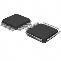


 工商网监
湘ICP备2023018690号
工商网监
湘ICP备2023018690号
