SN74SSQE32882
www.ti.com ................................................................................................................................................. SCAS857A – MARCH 2008 – REVISED OCTOBER 2008
28-BIT TO 56-BIT REGISTERED BUFFER WITH ADDRESS PARITY TEST
ONE PAIR TO FOUR PAIR DIFFERENTIAL CLOCK PLL DRIVER
FEATURES
1
• JEDEC SSTE32882 Compliant
• 1-to-2 Register Outputs and 1-to-4 Clock Pair
Outputs Support Stacked DDR3 DIMMs
• Chip Select Inputs Prevent Data Outputs from
Changing State and Minimize System Power
Consumption
• 1.5-V Phase Lock Loop Clock Driver Buffers
One Differential Clock Pair (CK and CK) and
Distributes to Four Differential Outputs
• 1.5-V CMOS Inputs
• Checks Parity on Command and Address
(CS-gated) Data Inputs
• Supports LVCMOS Switching Levels on
RESET Input
• RESET Input:
– Disables Differential Input Receivers
– Resets All Registers
– Forces All Outputs into Pre-defined States
• Optimal Pinout for DDR3 DIMM PCB Layout
• Supports Four Chip Selects
• Single Register Backside Mount Support
2
APPLICATIONS
•
•
DDR3 Registered DIMMs up to DDR3-1333
Single-, Dual- and Quad-Rank RDIMM
DESCRIPTION/ORDERING INFORMATION
This JEDEC SSTE32882-compliant, 28-bit 1:2 or
26-bit 1:2 and 4-bit 1:1 registering clock driver with
parity is designed for operation on DDR3 Registered
DIMMs up to DDR3-1333 with VDD of 1.5 V.
All inputs are 1.5-V, CMOS-compatible. All outputs
are 1.5-V CMOS drivers optimized to drive DRAM
signals on terminated traces in DDR3 RDIMM
applications. Clock outputs Yn and Yn and control net
outputs DxCKEn, DxCSn, and DxODTn can each be
driven with a different strength and skew to optimize
signal integrity, compensate for different loading, and
balance signal travel speed.
The SN74SSQE32882 has two basic modes of
operation associated with the Quad Chip Select
Enable (QCSEN) input.
First, when the QCSEN input pin is open or pulled
high, the component has two chip select inputs,
DCS0 and DCS1, and two copies of each chip select
output, QACS0, QACS1, QBCS0 and QBCS1. This
mode is the QuadCS disabled mode. Alternatively,
when the QCSEN input pin is pulled low, the
component has four chip select inputs DCS[3:0], and
four chip select outputs, QCS[3:0]. This mode is the
QuadCS enabled mode.
When QCSEN is high or floating, the device also
supports an operating mode that allows a single
device to be mounted on the back side of a DIMM
array. This device can then be configured to keep the
input bus termination (IBT) feature enabled for all
input signals independent of MIRROR. The
SN74SSQE32882. operates from a differential clock
(CK and CK). Data are registered at the crossing of
CK going high and CK going low. This data can either
be re-driven to the outputs or used to access internal
control registers. Details are covered in the Function
Tables (each flip-flop) with QCSEN = low.
Input bus data integrity is protected by a parity
function. All address and command input signals are
summed; the last bit of the sum is then compared to
the parity signal delivered by the system at the
PAR_IN input one clock cycle later. If these two
values do not match, the device pulls the open drain
output ERROUT low. The control signals (DCKE0,
DCKE1, DODT0, DODT1, and DCS[n:0]) are not part
of this computation.
The
SN74SSQE32882
implements
different
power-saving mechanisms to reduce thermal power
dissipation and to support system power-down states.
Power consumption is further reduced by disabling
unused outputs.
The package design is optimal for high-density
DIMMs. By aligning input and output positions
towards DIMM finger-signal ordering and SDRAM
ballout, the device de-scrambles the DIMM traces
and allows low crosstalk designs with low
interconnect latency. Edge-controlled outputs reduce
ringing and improve signal eye opening at the
SDRAM inputs.
1
2
Please be aware that an important notice concerning availability, standard warranty, and use in critical applications of Texas
Instruments semiconductor products and disclaimers thereto appears at the end of this data sheet.
All trademarks are the property of their respective owners.
PRODUCTION DATA information is current as of publication date.
Products conform to specifications per the terms of the Texas
Instruments standard warranty. Production processing does not
necessarily include testing of all parameters.
Copyright © 2008, Texas Instruments Incorporated
�SN74SSQE32882
SCAS857A – MARCH 2008 – REVISED OCTOBER 2008 ................................................................................................................................................. www.ti.com
These devices have limited built-in ESD protection. The leads should be shorted together or the device placed in conductive foam
during storage or handling to prevent electrostatic damage to the MOS gates.
ORDERING INFORMATION (1)
PACKAGE (2)
TCASE
0°C - Tcase
(see Table 1)
(1)
(2)
ORDERABLE
PART NUMBER
TOP-SIDE
MARKING
176ZAL
Tape and Reel
SN74SSQE32882ZALR
TE32882E
176ZCJ
Tape and Reel
SN74SSQE32882ZCJR
TE32882E
For the most current package and ordering information see the Package Option Addendum at the end of this document, or see the TI
web site at www.ti.com.
Package drawings, standard packing quantities, thermal data, symbolization, and PCB design guidelines are available at
www.ti.com/sc/package.
ELECTRICAL CHARACTERISTICS
ABSOLUTE MAXIMUM RATINGS
Over operating free-air temperature range (unless otherwise noted).
(1)
PARAMETER
VDD
Supply voltage
VI
Receiver input voltage
VREF
Reference voltage
VO
Driver output voltage
See
IIK
Input clamp current
IOK
IO
ICCC
Continuous current through each VDD or GND pin
Tstg
Storage temperature
(1)
(2)
(3)
See
(2)
(2)
and
and
(3)
(3)
VALUE
UNIT
–0.4 to +1.975
V
–0.4 to VDD + 0.5
V
–0.4 to VDD + 0.5
V
–0.4 to VDD + 0.5
V
VI < 0 or VI > VDD
–50
mA
Output clamp current
VO < 0 or VO > VDD
±50
mA
Continuous output current
0 < VO < VDD
±50
mA
±100
mA
–65 to +150
°C
Stresses beyond those listed under absolute maximum ratings may cause permanent damage to the device. These are stress ratings
only, and functional operation of the device at these or any other conditions beyond those indicated under operating conditions is not
implied. Exposure to absolute-maximum-rated conditions for extended periods may affect device reliability.
The input and output negative-voltage ratings may be exceeded if the input and output clamp-current ratings are observed.
This value is limited to 2.2 V maximum.
Table 1. Case Temperature vs Speed Node
PARAMETER
Tcase
(1)
2
Maximum case temperature
(1)
DDR3-800
DDR3-1066
DDR3-1333
DDR3-1600
UNIT
+109
+108
+106
+103
°C
The temperature values fit to JEDEC RAW cards A, B, and C. The user must keep Tcase below the specified values in order to keep the
junction temperature below +125°C. Other combinations of features and termination resistors can require lower case temperature and
extra cooling. These combinations depend on the specific application.
Submit Documentation Feedback
Copyright © 2008, Texas Instruments Incorporated
�SN74SSQE32882
www.ti.com ................................................................................................................................................. SCAS857A – MARCH 2008 – REVISED OCTOBER 2008
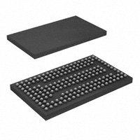
PACKAGE INFORMATION
ZAL Package
The package is an 8-mm × 13.5-mm, 176-pin ball grid array (BGA) with 0.65-mm ball pitch in an 11 × 20 grid.
The device pinout supports outputs on the outer two left and right columns to support easy DIMM signal routing.
Corresponding inputs are placed in such a way that two devices can be placed back-to-back for four rank
modules while the data inputs share the same vias. Each input and output is located close to an associated
no-ball position or on the outer two rows to allow for low-cost via technology combined with the small, 0.65-mm
ball pitch.
1
2
3
4
5
6
7
8
9
10 11
A
B
C
D
E
F
G
H
J
K
L
M
N
P
R
T
U
V
W
Y
Copyright © 2008, Texas Instruments Incorporated
Submit Documentation Feedback
3
�SN74SSQE32882
SCAS857A – MARCH 2008 – REVISED OCTOBER 2008 ................................................................................................................................................. www.ti.com
ZCJ Package
The package is an 6-mm × 15-mm, 176-pin ball grid array (BGA) with 0.65-mm ball pitch in an 8 × 22 grid. The
device pinout supports outputs on the outer two left and right columns to support easy DIMM signal routing.
Corresponding inputs are placed in such a way that two devices can be placed back-to-back for four rank
modules while the data inputs share the same vias.
1
2
3
4
5
6
7
8
A
B
C
D
E
F
G
H
J
K
L
M
N
P
R
T
U
V
W
Y
AA
AB
NOTE:
To request more information on SN74SSQE32882 DDR3 Register/PLL please contact
support@ti.com .
4
Submit Documentation Feedback
Copyright © 2008, Texas Instruments Incorporated
�PACKAGE OPTION ADDENDUM
www.ti.com
6-Oct-2015
PACKAGING INFORMATION
Orderable Device
Status
(1)
Package Type Package Pins Package
Drawing
Qty
SN74SSQE32882ZALR
NRND
NFBGA
ZAL
176
SN74SSQE32882ZCJR
NRND
NFBGA
ZCJ
176
2000
Eco Plan
Lead/Ball Finish
MSL Peak Temp
(2)
(6)
(3)
Op Temp (°C)
Green (RoHS
& no Sb/Br)
SNAGCU
Level-3-260C-168 HR
0 to 85
TBD
Call TI
Call TI
0 to 85
Device Marking
(4/5)
TE32882E
(1)
The marketing status values are defined as follows:
ACTIVE: Product device recommended for new designs.
LIFEBUY: TI has announced that the device will be discontinued, and a lifetime-buy period is in effect.
NRND: Not recommended for new designs. Device is in production to support existing customers, but TI does not recommend using this part in a new design.
PREVIEW: Device has been announced but is not in production. Samples may or may not be available.
OBSOLETE: TI has discontinued the production of the device.
(2)
Eco Plan - The planned eco-friendly classification: Pb-Free (RoHS), Pb-Free (RoHS Exempt), or Green (RoHS & no Sb/Br) - please check http://www.ti.com/productcontent for the latest availability
information and additional product content details.
TBD: The Pb-Free/Green conversion plan has not been defined.
Pb-Free (RoHS): TI's terms "Lead-Free" or "Pb-Free" mean semiconductor products that are compatible with the current RoHS requirements for all 6 substances, including the requirement that
lead not exceed 0.1% by weight in homogeneous materials. Where designed to be soldered at high temperatures, TI Pb-Free products are suitable for use in specified lead-free processes.
Pb-Free (RoHS Exempt): This component has a RoHS exemption for either 1) lead-based flip-chip solder bumps used between the die and package, or 2) lead-based die adhesive used between
the die and leadframe. The component is otherwise considered Pb-Free (RoHS compatible) as defined above.
Green (RoHS & no Sb/Br): TI defines "Green" to mean Pb-Free (RoHS compatible), and free of Bromine (Br) and Antimony (Sb) based flame retardants (Br or Sb do not exceed 0.1% by weight
in homogeneous material)
(3)
MSL, Peak Temp. - The Moisture Sensitivity Level rating according to the JEDEC industry standard classifications, and peak solder temperature.
(4)
There may be additional marking, which relates to the logo, the lot trace code information, or the environmental category on the device.
(5)
Multiple Device Markings will be inside parentheses. Only one Device Marking contained in parentheses and separated by a "~" will appear on a device. If a line is indented then it is a continuation
of the previous line and the two combined represent the entire Device Marking for that device.
(6)
Lead/Ball Finish - Orderable Devices may have multiple material finish options. Finish options are separated by a vertical ruled line. Lead/Ball Finish values may wrap to two lines if the finish
value exceeds the maximum column width.
Important Information and Disclaimer:The information provided on this page represents TI's knowledge and belief as of the date that it is provided. TI bases its knowledge and belief on information
provided by third parties, and makes no representation or warranty as to the accuracy of such information. Efforts are underway to better integrate information from third parties. TI has taken and
continues to take reasonable steps to provide representative and accurate information but may not have conducted destructive testing or chemical analysis on incoming materials and chemicals.
TI and TI suppliers consider certain information to be proprietary, and thus CAS numbers and other limited information may not be available for release.
Addendum-Page 1
Samples
�PACKAGE OPTION ADDENDUM
www.ti.com
6-Oct-2015
In no event shall TI's liability arising out of such information exceed the total purchase price of the TI part(s) at issue in this document sold by TI to Customer on an annual basis.
Addendum-Page 2
�PACKAGE MATERIALS INFORMATION
www.ti.com
24-Apr-2013
TAPE AND REEL INFORMATION
*All dimensions are nominal
Device
SN74SSQE32882ZALR
Package Package Pins
Type Drawing
NFBGA
ZAL
176
SPQ
Reel
Reel
A0
Diameter Width (mm)
(mm) W1 (mm)
2000
330.0
24.4
Pack Materials-Page 1
8.3
B0
(mm)
K0
(mm)
P1
(mm)
W
Pin1
(mm) Quadrant
13.8
1.8
12.0
24.0
Q1
�PACKAGE MATERIALS INFORMATION
www.ti.com
24-Apr-2013
*All dimensions are nominal
Device
Package Type
Package Drawing
Pins
SPQ
Length (mm)
Width (mm)
Height (mm)
SN74SSQE32882ZALR
NFBGA
ZAL
176
2000
336.6
336.6
31.8
Pack Materials-Page 2
���IMPORTANT NOTICE
Texas Instruments Incorporated and its subsidiaries (TI) reserve the right to make corrections, enhancements, improvements and other
changes to its semiconductor products and services per JESD46, latest issue, and to discontinue any product or service per JESD48, latest
issue. Buyers should obtain the latest relevant information before placing orders and should verify that such information is current and
complete. All semiconductor products (also referred to herein as “components”) are sold subject to TI’s terms and conditions of sale
supplied at the time of order acknowledgment.
TI warrants performance of its components to the specifications applicable at the time of sale, in accordance with the warranty in TI’s terms
and conditions of sale of semiconductor products. Testing and other quality control techniques are used to the extent TI deems necessary
to support this warranty. Except where mandated by applicable law, testing of all parameters of each component is not necessarily
performed.
TI assumes no liability for applications assistance or the design of Buyers’ products. Buyers are responsible for their products and
applications using TI components. To minimize the risks associated with Buyers’ products and applications, Buyers should provide
adequate design and operating safeguards.
TI does not warrant or represent that any license, either express or implied, is granted under any patent right, copyright, mask work right, or
other intellectual property right relating to any combination, machine, or process in which TI components or services are used. Information
published by TI regarding third-party products or services does not constitute a license to use such products or services or a warranty or
endorsement thereof. Use of such information may require a license from a third party under the patents or other intellectual property of the
third party, or a license from TI under the patents or other intellectual property of TI.
Reproduction of significant portions of TI information in TI data books or data sheets is permissible only if reproduction is without alteration
and is accompanied by all associated warranties, conditions, limitations, and notices. TI is not responsible or liable for such altered
documentation. Information of third parties may be subject to additional restrictions.
Resale of TI components or services with statements different from or beyond the parameters stated by TI for that component or service
voids all express and any implied warranties for the associated TI component or service and is an unfair and deceptive business practice.
TI is not responsible or liable for any such statements.
Buyer acknowledges and agrees that it is solely responsible for compliance with all legal, regulatory and safety-related requirements
concerning its products, and any use of TI components in its applications, notwithstanding any applications-related information or support
that may be provided by TI. Buyer represents and agrees that it has all the necessary expertise to create and implement safeguards which
anticipate dangerous consequences of failures, monitor failures and their consequences, lessen the likelihood of failures that might cause
harm and take appropriate remedial actions. Buyer will fully indemnify TI and its representatives against any damages arising out of the use
of any TI components in safety-critical applications.
In some cases, TI components may be promoted specifically to facilitate safety-related applications. With such components, TI’s goal is to
help enable customers to design and create their own end-product solutions that meet applicable functional safety standards and
requirements. Nonetheless, such components are subject to these terms.
No TI components are authorized for use in FDA Class III (or similar life-critical medical equipment) unless authorized officers of the parties
have executed a special agreement specifically governing such use.
Only those TI components which TI has specifically designated as military grade or “enhanced plastic” are designed and intended for use in
military/aerospace applications or environments. Buyer acknowledges and agrees that any military or aerospace use of TI components
which have not been so designated is solely at the Buyer's risk, and that Buyer is solely responsible for compliance with all legal and
regulatory requirements in connection with such use.
TI has specifically designated certain components as meeting ISO/TS16949 requirements, mainly for automotive use. In any case of use of
non-designated products, TI will not be responsible for any failure to meet ISO/TS16949.
Products
Applications
Audio
www.ti.com/audio
Automotive and Transportation
www.ti.com/automotive
Amplifiers
amplifier.ti.com
Communications and Telecom
www.ti.com/communications
Data Converters
dataconverter.ti.com
Computers and Peripherals
www.ti.com/computers
DLP® Products
www.dlp.com
Consumer Electronics
www.ti.com/consumer-apps
DSP
dsp.ti.com
Energy and Lighting
www.ti.com/energy
Clocks and Timers
www.ti.com/clocks
Industrial
www.ti.com/industrial
Interface
interface.ti.com
Medical
www.ti.com/medical
Logic
logic.ti.com
Security
www.ti.com/security
Power Mgmt
power.ti.com
Space, Avionics and Defense
www.ti.com/space-avionics-defense
Microcontrollers
microcontroller.ti.com
Video and Imaging
www.ti.com/video
RFID
www.ti-rfid.com
OMAP Applications Processors
www.ti.com/omap
TI E2E Community
e2e.ti.com
Wireless Connectivity
www.ti.com/wirelessconnectivity
Mailing Address: Texas Instruments, Post Office Box 655303, Dallas, Texas 75265
Copyright © 2015, Texas Instruments Incorporated
�


 工商网监
湘ICP备2023018690号
工商网监
湘ICP备2023018690号
