��������� ��������� ������
��� �
��
�
����
SLLS106G − DECEMBER 1975 − REVISED NOVEMBER 2004
D Improved Stability Over Supply Voltage and
D
D
D
D
Temperature Ranges
Constant-Current Outputs
High Speed
Standard Supply Voltages
High Output Impedance
High Common-Mode Output Voltage Range
. . . −3 V to 10 V
TTL-Input Compatibility
Inhibitor Available for Driver Selection
Glitch Free During Power Up/Power Down
SN75112 and External Circuit Meets or
Exceeds the Requirements of CCITT
Recommendation V.35
1A
1B
1C
2C
2A
2B
GND
1
14
2
13
3
12
4
11
5
10
6
9
7
8
VCC+
1Y
1Z
VCC−
D
2Z
2Y
SN55110A . . . FK PACKAGE
(TOP VIEW)
1B
1A
NC
V CC+
1Y
D
D
D
D
D
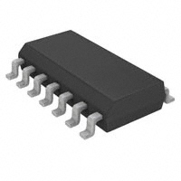
SN55110A . . . J OR W PACKAGE
SN75110A . . . D, N, OR NS PACKAGE
SN75112 . . . D OR N PACKAGE
(TOP VIEW)
description/ordering information
1C
NC
2C
NC
2A
3 2 1 20 19
18
5
17
6
16
7
15
8
14
9 10 11 12 13
1Z
NC
VCC−
NC
D
2B
GND
NC
2Y
2Z
The SN55110A, SN75110A, and SN75112 dual
line drivers have improved output current
regulation with supply-voltage and temperature
variations. In addition, the higher current of the
SN75112 (27 mA) allows data to be transmitted
over longer lines. These drivers offer optimum
performance when used with the SN55107A,
SN75107A, and SN75108A line receivers.
4
NC − No internal connection
ORDERING INFORMATION
PDIP (N)
0°C
0
C to 70
70°C
C
Tube of 25
SOIC (D)
SOP (NS)
−55°C to 125°C
ORDERABLE
PART NUMBER
PACKAGE†
TA
TOP-SIDE
MARKING
SN75110AN
SN75110AN
SN75112N
SN75112N
Tube of 50
SN75110AD
Reel of 2500
SN75110ADR
Tube of 50
SN75112D
Reel of 2500
SN75112DR
Reel of 2000
SN75110ANSR
SN75110A
SN55110AJ
SN55110AJ
SN75110A
SN75112
CDIP (J)
Tube of 25
SNJ55110AJ
SNJ55110AJ
CFP (W)
Tube of 150
SNJ55110AW
SNJ55110AW
LCCC (FK)
Tube of 55
SNJ55110AFK
SNJ55110AFK
† Package drawings, standard packing quantities, thermal data, symbolization, and PCB design guidelines
are available at www.ti.com/sc/package.
Please be aware that an important notice concerning availability, standard warranty, and use in critical applications of
Texas Instruments semiconductor products and disclaimers thereto appears at the end of this data sheet.
Copyright 2004, Texas Instruments Incorporated
���
���
��
��� ����������� �� ����!�� �� �� "�#$������� %��!&
���%���� ������� �� �"!����������� "!� �'! �!��� �� �!(��
������!���
����%��% )������*& ���%������ "���!����+ %�!� ��� �!�!�����$* ���$�%!
�!����+ �� �$$ "����!�!��&
�� "��%���� ���"$���� �� ,
�-��.-/0�/�� �$$ "����!�!�� ��! �!��!%
��$!�� ��'!�)��! ���!%& �� �$$ ��'!� "��%����� "��%������
"���!����+ %�!� ��� �!�!�����$* ���$�%! �!����+ �� �$$ "����!�!��&
POST OFFICE BOX 655303
• DALLAS, TEXAS 75265
1
���������� ��������� ������
��� �
��
�
����
SLLS106G − DECEMBER 1975 − REVISED NOVEMBER 2004
description/ordering information (continued)
These drivers feature independent channels with common voltage supply and ground terminals. The significant
difference between the three drivers is in the output-current specification. The driver circuits feature a constant
output current that is switched to either of two output terminals by the appropriate logic levels at the input
terminals. The output current can be switched off (inhibited) by low logic levels on the enable inputs. The output
current nominally is 12 mA for the ’110A devices and is 27 mA for the SN75112.
The enable/inhibit feature is provided so the circuits can be used in party-line or data-bus applications. A strobe
or inhibitor (enable D), common to both drivers, is included for increased driver-logic versatility. The output
current in the inhibited mode, IO(off), is specified so that minimum line loading is induced when the driver is used
in a party-line system with other drivers. The output impedance of the driver in the inhibited mode is very high.
The output impedance of a transistor is biased to cutoff.
The driver outputs have a common-mode voltage range of −3 V to 10 V, allowing common-mode voltage on the
line without affecting driver performance.
All inputs are diode clamped and are designed to satisfy TTL-system requirements. The inputs are tested at
2 V for high-logic-level input conditions and 0.8 V for low-logic-level input conditions. These tests ensure
400-mV noise margin when interfaced with TTL Series 54/74 devices.
The SN55110A is characterized for operation over the full military temperature range of −55°C to 125°C. The
SN75110A and SN75112 are characterized for operation from 0°C to 70°C.
FUNCTION TABLE
(each driver)
LOGIC
INPUTS
ENABLE
INPUTS
OUTPUTS†
A
B
C
D
Y
Z
X
X
L
X
Off
Off
X
X
X
L
Off
Off
Off
L
X
H
H
On
X
L
H
H
On
Off
H
H
H
H
Off
On
H = high level, L = low level, X = irrelevant
† When using only one channel of the line drivers,
the other channel should be inhibited and/or have
its outputs grounded.
2
POST OFFICE BOX 655303
• DALLAS, TEXAS 75265
���������� ��������� ������
��� �
��
�
����
SLLS106G − DECEMBER 1975 − REVISED NOVEMBER 2004
schematic (each driver)
VCC+
14
+
C
D
2.2 kΩ
NOM
3, 4
10
To Other
Driver
−
−
+
2.2 kΩ
NOM
8, 13
9, 12
A
B
GND
Y
Z
1, 5
2, 6
7
−
Common to Both Drivers
+
VCC−
11
−
+
. . . VCC+ Bus
−
. . . VCC− Bus
−
To Other Driver
Pin numbers shown are for the D, J, N, NS, and W packages.
POST OFFICE BOX 655303
• DALLAS, TEXAS 75265
3
���������� ��������� ������
��� �
��
�
����
SLLS106G − DECEMBER 1975 − REVISED NOVEMBER 2004
absolute maximum ratings over operating free-air temperature (unless otherwise noted)†
Supply voltage: VCC+ (see Note 1) . . . . . . . . . . . . . . . . . . . . . . . . . . . . . . . . . . . . . . . . . . . . . . . . . . . . . . . . . . . . 7 V
VCC− (see Note 1) . . . . . . . . . . . . . . . . . . . . . . . . . . . . . . . . . . . . . . . . . . . . . . . . . . . . . . . . . . −7 V
Input voltage, VI . . . . . . . . . . . . . . . . . . . . . . . . . . . . . . . . . . . . . . . . . . . . . . . . . . . . . . . . . . . . . . . . . . . . . . . . . . 5.5 V
Output voltage range, VO . . . . . . . . . . . . . . . . . . . . . . . . . . . . . . . . . . . . . . . . . . . . . . . . . . . . . . . . . . . . −5 V to 12 V
Package thermal impedance, θJA (see Notes 2 and 3): D package . . . . . . . . . . . . . . . . . . . . . . . . . . . . 86°C/W
N package . . . . . . . . . . . . . . . . . . . . . . . . . . . . 80°C/W
NS package . . . . . . . . . . . . . . . . . . . . . . . . . . . 76°C/W
Package thermal impedance, θJC (see Notes 4 and 5): FK package . . . . . . . . . . . . . . . . . . . . . . . . 13.42°C/W
J package . . . . . . . . . . . . . . . . . . . . . . . . . 15.05°C/W
W package . . . . . . . . . . . . . . . . . . . . . . . . 14.65°C/W
Operating virtual junction temperature . . . . . . . . . . . . . . . . . . . . . . . . . . . . . . . . . . . . . . . . . . . . . . . . . . . . . . 150°C
Case temperature for 60 seconds: FK package . . . . . . . . . . . . . . . . . . . . . . . . . . . . . . . . . . . . . . . . . . . . . . 260°C
Lead temperature 1,6 mm (1/16 inch) from case for 60 seconds: J or W package . . . . . . . . . . . . . . . . 300°C
Storage temperature range, Tstg . . . . . . . . . . . . . . . . . . . . . . . . . . . . . . . . . . . . . . . . . . . . . . . . . . −65°C to 150°C
† Stresses beyond those listed under “absolute maximum ratings” may cause permanent damage to the device. These are stress ratings only, and
functional operation of the device at these or any other conditions beyond those indicated under “recommended operating conditions” is not
implied. Exposure to absolute-maximum-rated conditions for extended periods may affect device reliability.
NOTES: 1. Voltage values are with respect to network ground terminal.
2. Maximum power dissipation is a function of TJ(max), θJA, and TA. The maximum allowable power dissipation at any allowable
ambient temperature is PD = (TJ(max) − TA)/θJA. Operating at the absolute maximum TJ of 150°C can affect reliability.
3. The package thermal impedance is calculated in accordance with JESD 51-7.
4. Maximum power dissipation is a function of TJ(max), θJC, and TC. The maximum allowable power dissipation at any allowable case
temperature is PD = (TJ(max) − TC)/θJC. Operating at the absolute maximum TJ of 150°C can affect reliability.
5. The package thermal impedance is calculated in accordance with MIL-STD-883.
recommended operating conditions (see Note 6)
SN75110A
SN75112
SN55110A
MIN
VCC+
VCC−
VIH
VIL
NOM
MAX
MIN
NOM
UNIT
MAX
Supply voltage
4.5
5
5.5
4.75
5
5.25
V
Supply voltage
−4.5
−5
−5.5
−4.75
−5
−5.25
V
Positive common-mode output voltage
0
10
0
10
V
Negative common-mode output voltage
0
−3
0
−3
V
High-level input voltage
2
2
0.8
V
0.8
V
TA
Operating free-air temperature
−55
125
0
70
NOTE 6: When using only one channel of the line drivers, the other channel should be inhibited and/or have its outputs grounded.
°C
4
Low-level output voltage
POST OFFICE BOX 655303
• DALLAS, TEXAS 75265
���������� ��������� ������
��� �
��
�
����
SLLS106G − DECEMBER 1975 − REVISED NOVEMBER 2004
electrical characteristics over recommended operating free-air temperature range (unless
otherwise noted)
SN55110A
SN75110A
TEST CONDITIONS†
PARAMETER
MIN
VIK
Input clamp voltage
IO(on)
On-state output current
VCC± = MIN,
VCC± = MAX,
SN75112
TYP‡
MAX
−0.9
12
IL = −12 mA
VO = 10 V
MAX
−1.5
−0.9
−1.5
15
27
40
24
28
32
mA
15
27
100
100
µA
1
1
2
2
40
40
80
80
−3
−3
−6
−6
VCC = MIN to MAX,
VO = −1 V to 1 V, TA = 25°C
VCC± = MIN,
VCC± = MIN,
VO = −3 V
VO = 10 V
VCC±
CC = MAX,
VI = 5.5 V
VCC±
CC = MAX,
VI = 2.4 V
VCC±
CC = MAX,
VI = 0.4 V
6.5
UNIT
TYP‡
12
MIN
V
IO(off)
Off-state output current
A, B, or C inputs
II
Input current
at maximum
input voltage
High-level
input current
A, B, or C inputs
IIH
Low-level
input current
A, B, or C inputs
IIL
ICC+(on)
Supply current from VCC
with driver enabled
VCC± = MAX,
A and B inputs at 0.4 V,
C and D inputs at 2 V
23
35
25
40
mA
ICC−(on)
Supply current from VCC−
with driver enabled
VCC±
CC = MAX,
A and B inputs at 0.4 V,
C and D inputs at 2 V
−34
−50
−65
−100
mA
ICC+(off)
Supply current from VCC−
with driver inhibited
VCC± = MAX,
A, B, C, and D inputs at 0.4 V
21
30
mA
ICC−(off)
Supply current from VCC±
with driver inhibited
VCC± = MAX,
A, B, C, and D inputs at 0.4 V
−17
−32
mA
D input
D input
D input
mA
µA
A
mA
† For conditions shown as MIN or MAX, use appropriate value specified under recommended operating conditions.
‡ All typical values are at VCC+ = 5 V, VCC− = −5 V, TA = 25°C.
switching characteristics, VCC± = ±5 V, TA = 25°C (see Figure 1)
PARAMETER§
FROM
(INPUT)
TO
(OUTPUT)
tPLH
tPHL
A or B
Y or Z
CL = 40 pF,
Ω
RL = 50 Ω,
tPLH
tPHL
C or D
Y or Z
CL = 40 pF,
RL = 50 Ω
Ω,
TEST CONDITIONS
MIN
TYP
MAX
9
15
9
15
16
25
13
25
UNIT
ns
ns
§ tPLH = propagation delay time, low- to high-level output
tPHL = propagation delay time, high- to low-level output
POST OFFICE BOX 655303
• DALLAS, TEXAS 75265
5
���������� ��������� ������
��� �
��
�
����
SLLS106G − DECEMBER 1975 − REVISED NOVEMBER 2004
PARAMETER MEASUREMENT INFORMATION
VCC+
Input A or B
VCC−
50 Ω
890 Ω
890 Ω
Output Y
RL = 50 Ω
CL = 40 pF
(see Note A)
RL = 50 Ω
CL = 40 pF
(see Note A)
Pulse
Generator
(See Note B)
Output Z
Pulse
Generator
(See Note B)
To Other Driver
Input C or D
See Note C
50 Ω
TEST CIRCUIT
3V
50%
Input A or B
50%
0V
tw1
tw2
3V
50%
Enable C or D
50%
0V
tPLH
tPHL
tPLH
tPHL
Off
Output Y
50%
50%
50%
50%
On
tPHL
tPLH
Off
Output Z
50%
50%
On
VOLTAGE WAVEFORMS
NOTES: A. CL includes probe and jig capacitance.
B. The pulse generators have the following characteristics: ZO = 50 Ω, tr = tf = 10 ± 5 ns, tw1 = 500 ns, PRR ≤ 1 MHz, tw2 = 1 µs,
PRR ≤ 500 kHz.
C. For simplicity, only one channel and the enable connections are shown.
Figure 1. Test Circuit and Voltage Waveforms
6
POST OFFICE BOX 655303
• DALLAS, TEXAS 75265
���������� ��������� ������
��� �
��
�
����
SLLS106G − DECEMBER 1975 − REVISED NOVEMBER 2004
TYPICAL CHARACTERISTICS
SN75112
ON-STATE OUTPUT CURRENT
vs
NEGATIVE SUPPLY VOLTAGE
SN55110A, SN75110A
ON-STATE OUTPUT CURRENT
vs
NEGATIVE SUPPLY VOLTAGE
35
VCC+ = 4.5 V
VO = −3 V
TA = 25°C
12
I O(on) − On-State Output Current − mA
I O(on) − On-State Output Current − mA
14
10
8
6
4
2
0
−3
−4
−5
−6
−7
30
VCC+ = 4.5 V
VO = −3 V
TA = 25°C
25
20
15
10
5
0
−3
VCC− − Negative Supply Voltage − V
−4
−5
−6
−7
VCC− − Negative Supply Voltage − V
Figure 2
Figure 3
POST OFFICE BOX 655303
• DALLAS, TEXAS 75265
7
���������� ��������� ������
��� �
��
�
����
SLLS106G − DECEMBER 1975 − REVISED NOVEMBER 2004
APPLICATION INFORMATION
special pulse-control circuit
Figure 4 shows a circuit that can be used as a pulse-generator output or in many other testing applications.
INPUT
A
High
Low
OUTPUTS
Z
Y
Off
On
On
Off
5V
2
3
3
4
VCC+
Y
A
Input
1
5
2
5
1
6
4
6
B
2.5 V
Z
C
D
3
1/2 ’110A
or SN75112
GND
4
5
2
VCC−
6
1
−5 V
To Other Logic and
Strobe Inputs
Output
Input Pulse
0V
Switch
Position
1
2
3
4
Output Pulse
6
0V
Figure 4. Pulse-Control Circuit
8
5
POST OFFICE BOX 655303
• DALLAS, TEXAS 75265
���������� ��������� ������
��� �
��
�
����
SLLS106G − DECEMBER 1975 − REVISED NOVEMBER 2004
APPLICATION INFORMATION
using the SN75112 as a CCITT-recommended V.35 line driver
The SN75112 dual line driver, the SN75107A dual line receiver, and some external resistors can be used to
implement the data-interchange circuit of CCITT recommendation V.35 (1976) modem specification. The circuit
of one channel is shown in Figure 5 and meets the requirement of the interface as specified by Appendix 11
of CCITT V.35 and is summarized in Table 1 (V.35 has been replaced by ITU V.11).
Table 1. CCITT V.35 Electrical Requirements
GENERATOR
MIN
MAX
UNIT
50
150
Ω
Resistance to ground, R
135
165
Ω
Differential output voltage, VOD
440
660
mV
Source impedance, Zsource
10% to 90% rise time, tr
40
ns
0.01 × ui†
or
Common-mode output voltage, VOC
−0.6
0.6
LOAD (RECEIVER)
MIN
MAX
Input impedance, ZI
90
110
Ω
Resistance to ground, R
135
165
† ui = unit interval or minimum signal-element pulse duration
Ω
5V
V
UNIT
5V
5V
R3
390 Ω
100 pF
1/2 SN75112
13 1Y
1
1A
2
Data In
1B
10
Enable
1C
R1
1.3 kΩ
R5
75 Ω
12
1Z
3
100 pF
R4
390 Ω
All resistors are 5%, 1/4 W.
Strobe
R6
50 Ω
R8
125 Ω
R7
50 Ω
6
1A 1
2
1B
4 Data Out
1Y
5 Enable
1G
1/2 SN75107A
R2
1.3 kΩ
5V
Figure 5. CCITT-Recommended V.35 Interface Using the SN75112 and SN75107A
POST OFFICE BOX 655303
• DALLAS, TEXAS 75265
9
�PACKAGE OPTION ADDENDUM
www.ti.com
10-Jun-2022
PACKAGING INFORMATION
Orderable Device
Status
(1)
Package Type Package Pins Package
Drawing
Qty
Eco Plan
(2)
Lead finish/
Ball material
MSL Peak Temp
Op Temp (°C)
Device Marking
(3)
Samples
(4/5)
(6)
5962-87547012A
ACTIVE
LCCC
FK
20
1
Non-RoHS
& Green
SNPB
N / A for Pkg Type
-55 to 125
596287547012A
SNJ55
110AFK
5962-8754701CA
ACTIVE
CDIP
J
14
1
Non-RoHS
& Green
SNPB
N / A for Pkg Type
-55 to 125
5962-8754701CA
SNJ55110AJ
Samples
5962-8754701DA
ACTIVE
CFP
W
14
1
Non-RoHS
& Green
SNPB
N / A for Pkg Type
-55 to 125
5962-8754701DA
SNJ55110AW
Samples
SN55110AJ
ACTIVE
CDIP
J
14
1
Non-RoHS
& Green
SNPB
N / A for Pkg Type
-55 to 125
SN55110AJ
Samples
SN75110AD
ACTIVE
SOIC
D
14
50
RoHS & Green
NIPDAU
Level-1-260C-UNLIM
0 to 70
SN75110A
Samples
SN75110ADR
ACTIVE
SOIC
D
14
2500
RoHS & Green
NIPDAU
Level-1-260C-UNLIM
0 to 70
SN75110A
Samples
SN75110AN
ACTIVE
PDIP
N
14
25
RoHS & Green
NIPDAU
N / A for Pkg Type
0 to 70
SN75110AN
Samples
SN75110ANSR
ACTIVE
SO
NS
14
2000
RoHS & Green
NIPDAU
Level-1-260C-UNLIM
0 to 70
SN75110A
Samples
SN75112D
ACTIVE
SOIC
D
14
50
RoHS & Green
NIPDAU
Level-1-260C-UNLIM
0 to 70
SN75112
Samples
SN75112DR
ACTIVE
SOIC
D
14
2500
RoHS & Green
NIPDAU
Level-1-260C-UNLIM
0 to 70
SN75112
Samples
SN75112N
ACTIVE
PDIP
N
14
25
RoHS & Green
NIPDAU
N / A for Pkg Type
0 to 70
SN75112N
Samples
SNJ55110AFK
ACTIVE
LCCC
FK
20
1
Non-RoHS
& Green
SNPB
N / A for Pkg Type
-55 to 125
596287547012A
SNJ55
110AFK
SNJ55110AJ
ACTIVE
CDIP
J
14
1
Non-RoHS
& Green
SNPB
N / A for Pkg Type
-55 to 125
5962-8754701CA
SNJ55110AJ
Samples
SNJ55110AW
ACTIVE
CFP
W
14
1
Non-RoHS
& Green
SNPB
N / A for Pkg Type
-55 to 125
5962-8754701DA
SNJ55110AW
Samples
(1)
The marketing status values are defined as follows:
ACTIVE: Product device recommended for new designs.
LIFEBUY: TI has announced that the device will be discontinued, and a lifetime-buy period is in effect.
NRND: Not recommended for new designs. Device is in production to support existing customers, but TI does not recommend using this part in a new design.
Addendum-Page 1
Samples
Samples
�PACKAGE OPTION ADDENDUM
www.ti.com
10-Jun-2022
PREVIEW: Device has been announced but is not in production. Samples may or may not be available.
OBSOLETE: TI has discontinued the production of the device.
(2)
RoHS: TI defines "RoHS" to mean semiconductor products that are compliant with the current EU RoHS requirements for all 10 RoHS substances, including the requirement that RoHS substance
do not exceed 0.1% by weight in homogeneous materials. Where designed to be soldered at high temperatures, "RoHS" products are suitable for use in specified lead-free processes. TI may
reference these types of products as "Pb-Free".
RoHS Exempt: TI defines "RoHS Exempt" to mean products that contain lead but are compliant with EU RoHS pursuant to a specific EU RoHS exemption.
Green: TI defines "Green" to mean the content of Chlorine (Cl) and Bromine (Br) based flame retardants meet JS709B low halogen requirements of