SN75207B
DUAL SENSE AMPLIFIER FOR MOS MEMORIES
OR DUAL HIGH-SENSITIVITY LINE RECEIVERS
SLLS096C – JULY 1973 – REVISED MARCH 1997
D
D
D
D
D
D
D
D
D
D
D
Plug-In Replacement for SN75107A and
SN75107B With Improved Characteristics
± 10-mV Input Sensitivity
TTL-Compatible Circuitry
Standard Supply Voltages . . . ± 5 V
Differential Input Common-Mode Voltage
Range of ± 3 V
Strobe Inputs for Channel Selection
Totem-Pole Outputs
SN75207B Has Diode-Protected Input Stage
for Power-Off Condition
Sense Amplifier for MOS Memories
Dual Comparator
High-Sensitivity Line Receiver
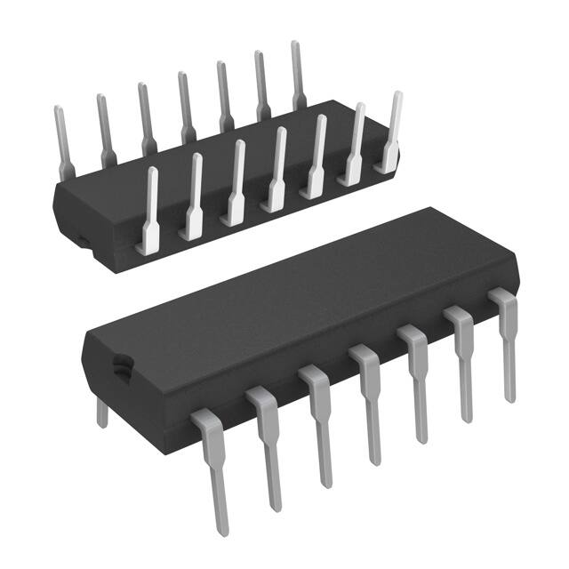
N PACKAGE
(TOP VIEW)
1A
1B
NC
1Y
1G
S
GND
1
14
2
13
3
12
4
11
5
10
6
9
7
8
VCC +
VCC –
2A
2B
NC
2Y
2G
NC – No internal connection
description
The SN75207B is a terminal-for-terminal replacement for the SN75107B. The improved input sensitivity makes
it more suitable for MOS memory sense amplifiers and can result in faster memory cycles. Improved sensitivity
also makes it more useful in line-receiver applications by allowing use of longer transmission line lengths. The
SN75207B features a TTL-compatible, active-pullup output.
Input protection diodes are in series with the collectors of the differential-input transistors of the SN75207B.
These diodes are useful in certain party-line systems that may have multiple VCC + power supplies and may be
operated with some of the VCC + supplies turned off. In such a system, if a supply is turned off and allowed to
go to ground, the equivalent input circuit connected to that supply would be as follows:
Input
SN75207B
This would be a problem in specific systems that might have the transmission lines biased to some potential
greater than 1.4 V.
This device is characterized for operation from 0°C to 70°C.
FUNCTION TABLE
DIFFERENTIAL INPUTS
A–B
VID ≥ 10 mV
– 10 mV < VID < 10 mV
VID ≤ –10 mV
STROBES
G
S
OUTPUT
Y
X
X
H
X
L
H
L
X
H
H
H
Indeterminate
X
L
H
L
X
H
H
H
L
H = high level, L = low level, X = irrelevant
Please be aware that an important notice concerning availability, standard warranty, and use in critical applications of
Texas Instruments semiconductor products and disclaimers thereto appears at the end of this data sheet.
Copyright 1997, Texas Instruments Incorporated
PRODUCTION DATA information is current as of publication date.
Products conform to specifications per the terms of Texas Instruments
standard warranty. Production processing does not necessarily include
testing of all parameters.
POST OFFICE BOX 655303
• DALLAS, TEXAS 75265
1
�SN75207B
DUAL SENSE AMPLIFIER FOR MOS MEMORIES
OR DUAL HIGH-SENSITIVITY LINE RECEIVERS
SLLS096C – JULY 1973 – REVISED MARCH 1997
logic symbol†
S
1A
6
logic diagram (positive logic)
EN
S
1A
&
1
6
1
4 1Y
2
1B
5
1G
12
2A
11
2B
8
2G
1B
1G
9 2Y
2G
† This symbol is in accordance with ANSI/IEEE Std 91-1984
and IEC Publication 617-12.
2A
2B
4
2
1Y
5
8
12
9
2Y
11
schematic (each receiver)
VCC +
14
1 kΩ
400 Ω
1 kΩ
1.6 kΩ
4 kΩ
120 Ω
4.8 kΩ
800 Ω
A
1, 12
760 Ω
1 kΩ
Inputs
B
2, 11
4.25 kΩ
Y
GND
ÁÁ
ÁÁ
G
3 kΩ
Common
To Both
Receivers
ÁÁ
6
13
S
To Other Receiver
Resistor values shown are nominal.
2
7
5, 8
3 kΩ
VCC –
ÁÁ
ÁÁ
4, 9
POST OFFICE BOX 655303
• DALLAS, TEXAS 75265
�SN75207B
DUAL SENSE AMPLIFIER FOR MOS MEMORIES
OR DUAL HIGH-SENSITIVITY LINE RECEIVERS
SLLS096C – JULY 1973 – REVISED MARCH 1997
design characteristics
The SN75207B line receivers/sense amplifiers are TTL-compatible, dual circuits intended for use in high-speed,
data-transmission systems or MOS memory systems. They are designed to detect low-level differential signals
in the presence of common-mode noise and variations of temperature and supplies. The dc specifications
reflect worst-case conditions of temperature, supply voltages, and input voltages.
The input common-mode voltage range is ± 3 V. This is adequate for application in most systems. In systems
with requirements for greater common-mode voltage range, input attenuators may be used to decrease the
noise to an acceptable level at the receiver-input terminals.
The circuits feature individual strobe inputs for each channel and a strobe input common to both channels for
logic versatility. The strobe inputs are tested to ensure 400 mV of dc noise margin when interfaced with Series
54/74 TTL.
The circuits feature high input impedance and low input currents, which induce very little loading on the
transmission line. This makes these devices especially useful in party-line systems. The excellent input
sensitivity (3 mV typical) is particularly important when data is to be detected at the end of a long transmission
line and the amplitude of the data has deteriorated due to cable losses. The circuits are designed to detect input
signals of 10-mV (or greater) amplitude and convert the polarity of the signal into appropriate TTL-compatible
output logic levels.
absolute maximum ratings over operating free-air temperature range (unless otherwise noted)†
Supply voltage, VCC + (see Note 1) . . . . . . . . . . . . . . . . . . . . . . . . . . . . . . . . . . . . . . . . . . . . . . . . . . . . . . . . . . . . 7 V
Supply voltage, VCC – (see Note 1) . . . . . . . . . . . . . . . . . . . . . . . . . . . . . . . . . . . . . . . . . . . . . . . . . . . . . . . . . . . – 7 V
Differential input voltage, VID (see Note 2) . . . . . . . . . . . . . . . . . . . . . . . . . . . . . . . . . . . . . . . . . . . . . . . . . . . . ± 6 V
Common-mode input voltage, VIC (see Note 3) . . . . . . . . . . . . . . . . . . . . . . . . . . . . . . . . . . . . . . . . . . . . . . . . ± 5 V
Strobe input voltage . . . . . . . . . . . . . . . . . . . . . . . . . . . . . . . . . . . . . . . . . . . . . . . . . . . . . . . . . . . . . . . . . . . . . . . 5.5 V
Continuous total dissipation . . . . . . . . . . . . . . . . . . . . . . . . . . . . . . . . . . . . . . . . . . . See Dissipation Rating Table
Operating free-air temperature range, TA . . . . . . . . . . . . . . . . . . . . . . . . . . . . . . . . . . . . . . . . . . . . . . 0°C to 70°C
Storage temperature range, Tstg . . . . . . . . . . . . . . . . . . . . . . . . . . . . . . . . . . . . . . . . . . . . . . . . . . . – 65°C to 150°C
Lead temperature 1,6 mm (1/16 inch) from case for 10 seconds . . . . . . . . . . . . . . . . . . . . . . . . . . . . . . . 260°C
† Stresses beyond those listed under “absolute maximum ratings” may cause permanent damage to the device. These are stress ratings only, and
functional operation of the device at these or any other conditions beyond those indicated under “recommended operating conditions” is not
implied. Exposure to absolute-maximum-rated conditions for extended periods may affect device reliability.
NOTES: A. All voltage values, except differential voltages, are with respect to GND terminal.
1. Differential input voltage values are at the noninverting (A) terminal with respect to the inverting (B) terminal.
2. Common-mode input voltage is the average of the voltages at the A and B inputs.
DISSIPATION RATING TABLE
PACKAGE
TA ≤ 25°C
POWER RATING
DERATING FACTOR
ABOVE TA = 25°C
TA = 70°C
POWER RATING
N
1050 mW
9.2 mW/°C
636 mW
POST OFFICE BOX 655303
• DALLAS, TEXAS 75265
3
�SN75207B
DUAL SENSE AMPLIFIER FOR MOS MEMORIES
OR DUAL HIGH-SENSITIVITY LINE RECEIVERS
SLLS096C – JULY 1973 – REVISED MARCH 1997
recommended operating conditions (see Note 4)
MIN
NOM
MAX
UNIT
Supply voltage, VCC +
4.75
5
5.25
V
Supply voltage, VCC –
– 4.75
–5
– 5.25
V
High-level differential input voltage, VID(H) (see Note 5)
5
V
Low-level differential input voltage, VID(L)
0.01
– 5†
– 0.01
V
Common-mode input voltage, VIC (see Notes 5 and 6)
– 3†
3
V
Input voltage, any differential input to ground (see Note 5)
– 5†
3
V
High-level input voltage at strobe inputs, VIH(S)
2
5.5
V
Low-level input voltage at strobe inputs, VIL(S)
0
0.8
V
–16
mA
Low-level output current, IOL
Operating free-air temperature, TA
0
70
°C
† The algebraic convention, in which the less positive (more negative) limit is designated as minimum, is used in this data sheet for logic voltage
levels only.
NOTES: B. When using only one channel of the line receiver, the strobe G of the unused channel should be grounded and at least one of the
differential inputs of the unused receiver should be terminated at some voltage between – 3 V and 3 V.
3. The recommended combinations of input voltages fall within the shaded area of the figure shown.
4. The common-mode voltage may be as low as – 4 V provided that the more positive of the two inputs is not more negative than – 3 V.
Inputs – A-to-Ground Voltage – V
3
2
1
0
–1
–2
–3
–4
–5
–5
–4
–3
–2
–1
0
1
2
Inputs – B-to-Ground Voltage – V
4
POST OFFICE BOX 655303
• DALLAS, TEXAS 75265
3
�SN75207B
DUAL SENSE AMPLIFIER FOR MOS MEMORIES
OR DUAL HIGH-SENSITIVITY LINE RECEIVERS
SLLS096C – JULY 1973 – REVISED MARCH 1997
electrical characteristics over recommended free-air temperature range (unless otherwise noted)
PARAMETER
TEST CONDITIONS
MIN
Low-level input current
VCC± = ± 5.25 V
VCC± = ± 5.25 V
IIH
High-level
g
input current
into 1G or 2G
VCC± = ± 5.25 V,
VCC± = ± 5.25 V,
VIH(S) = 2.4 V
VIH(S) = ± 5.25 V
IIL
Low-level input current
into 1G or 2G
VCC± = ± 5.25
5 25 V,
V
VIL(S) = 0
0.4
4V
IIH
High level input current into S
High-level
VCC± = ± 5.25 V,
VCC± = ± 5.25 V,
VIH(S) = 2.4 V
VIH(S) = ± 5.25 V
IIL
Low-level input current into S
VCC± = ± 5.25 V,
VIL(S) = 0.4 V
VOH
High level output voltage
High-level
VCC± = ± 4.75 V,,
IOH = – 400 µA,
VIL(S) = 0.8 V,,
VIC = – 3 V to 3 V
VID(H) = 10 mV,,
VOL
Low level output voltage
Low-level
VCC± = ± 4.75 V,,
IOL = 16 mA,
VIH(S) = 2 V,,
VIC = – 3 V to 3 V
VID(L) = –10 mV,,
IOH
High-level output current
VCC± = ± 4.75 V,
VOH = ± 5.25 V
IOS
Short-circuit output current‡
VCC± = ± 5.25 V
IIH
IIL
High-level input current
VID = – 5 V
VID = 5 V
TYP†
MAX
30
75
µA
–10
µA
40
µA
1
mA
–1.6
16
mA
80
µA
2
mA
– 3.2
mA
24
2.4
V
04
0.4
–18
ICC+
Supply current from VCC +
VCC± = ± 5.25 V,
TA = 25°C,
ICC –
Supply current from VCC –
VCC± = ± 5.25 V,
TA = 25°C,
† All typical values are at VCC + = 5 V, VCC – = – 5 V, TA = 25°C.
‡ Not more than one output should be shorted at a time.
UNIT
V
400
µA
–70
mA
Outputs high
18
30
mA
Outputs high
– 8.4
–15
mA
MIN
MAX
UNIT
switching characteristics, VCC+ = 5 V, VCC– = –5 V, TA = 25°C
TEST
CONDITIONS
PARAMETER
tPLH(D)
tPHL(D)
Propagation delay time, low- to high-level output, from differential inputs A and B
Propagation delay time, high- to low-level output, from differential inputs A and B
tPLH(S)
Propagation delay time, low- to high-level output, from strobe
input G or S
tPHL(S)
Propagation delay time, high- to low-level output, from strobe
input G or S
POST OFFICE BOX 655303
RL = 470 Ω,
See Figure 1
• DALLAS, TEXAS 75265
CL = 50 pF,
35
ns
20
ns
17
ns
17
ns
5
�SN75207B
DUAL SENSE AMPLIFIER FOR MOS MEMORIES
OR DUAL HIGH-SENSITIVITY LINE RECEIVERS
SLLS096C – JULY 1973 – REVISED MARCH 1997
PARAMETER MEASUREMENT INFORMATION
VCC –
Differential
Input
Output
1A
1Y
1B
Pulse
Generator
(see Note A)
50 Ω
Vref
100 mV
CL = 50 pF
(see Note C)
2A
See Note D
2B
2Y
1G
Strobe
Input
(see Note B)
S
2G
470 Ω
VCC+
50 Ω
Pulse
Generator
(see Note A)
TEST CIRCUIT
40 mV
B
40 mV
10 mV
10 mV
0V
tw1
tw2
3V
3V
1.5 V
tPLH(D)
G or S
1.5 V
tPHL(D)
0V
tPLH(S)
VOH
1.5 V
Y
tPHL(S)
1.5 V
VOH
1.5 V
1.5 V
VOL
VOL
VOLTAGE WAVEFORMS
NOTES: A. The pulse generators have the following characteristics: ZO = 50 Ω, tr ≤ 5 ns, tf ≤ 5 ns, tw1 = 500 ns with PRR = 1 MHz, tw2 = 1 µs
with PRR = 500 kHz.
B. Strobe input pulse is applied to Strobe 1G when inputs 1A–1B are being tested, to Strobe S when inputs 1A–1B or 2A–2B are being
tested, and to Strobe 2G when inputs 2A–2B are being tested.
C. CL includes probe and jig capacitance.
D. All diodes are 1N916.
Figure 1. Test Circuit and Voltage Waveforms
6
POST OFFICE BOX 655303
• DALLAS, TEXAS 75265
�SN75207B
DUAL SENSE AMPLIFIER FOR MOS MEMORIES
OR DUAL HIGH-SENSITIVITY LINE RECEIVERS
SLLS096C – JULY 1973 – REVISED MARCH 1997
APPLICATION INFORMATION
Strobes
100 Ω
Input
From
TTL
SN75361A
or
SN75452B
MOS Memory
Output
to TTL
To
Dummy
Line
100 Ω
’207B
Vref
Adjustment
Drive
Memory
Sense
Figure 2. MOS Memory Sense Amplifier
Receiver 1
Receiver 2
Receiver 4
Y
Y
Y
Strobes
Transmission Line Having
Characteristics Impedance ZO
Strobes
RT
Strobes
RT
RT
RT
Location 2
Driver 3
Driver 1
Driver 4
Data Input
A
B
A
B
A
B
Inhibit
C
D
C
D
C
D
Location 1
Location 3
Location 4
Receivers are SN75207B; drivers are SN55109A, SN55110A, SN75110A, or SN75112.
Figure 3. Data-Bus or Parity-Line System
PRECAUTIONS: When only one receiver in a package is being used, at least one of the differential inputs of the
unused receiver should be terminated at some voltage between – 3 V and 3 V, preferably at GND. Failure to do so
will cause improper operation of the unit being used because of common bias circuitry for the current sources of the
two receivers. Strobe G of the unused channel should be grounded.
POST OFFICE BOX 655303
• DALLAS, TEXAS 75265
7
�PACKAGE OPTION ADDENDUM
www.ti.com
23-Apr-2022
PACKAGING INFORMATION
Orderable Device
Status
(1)
Package Type Package Pins Package
Drawing
Qty
Eco Plan
(2)
Lead finish/
Ball material
MSL Peak Temp
Op Temp (°C)
Device Marking
(3)
(4/5)
(6)
SN75207BN
ACTIVE
PDIP
N
14
25
RoHS & Green
NIPDAU
N / A for Pkg Type
0 to 70
SN75207BN
SN75207BNSR
ACTIVE
SO
NS
14
2000
RoHS & Green
NIPDAU
Level-1-260C-UNLIM
0 to 70
SN75207B
(1)
The marketing status values are defined as follows:
ACTIVE: Product device recommended for new designs.
LIFEBUY: TI has announced that the device will be discontinued, and a lifetime-buy period is in effect.
NRND: Not recommended for new designs. Device is in production to support existing customers, but TI does not recommend using this part in a new design.
PREVIEW: Device has been announced but is not in production. Samples may or may not be available.
OBSOLETE: TI has discontinued the production of the device.
(2)
RoHS: TI defines "RoHS" to mean semiconductor products that are compliant with the current EU RoHS requirements for all 10 RoHS substances, including the requirement that RoHS substance
do not exceed 0.1% by weight in homogeneous materials. Where designed to be soldered at high temperatures, "RoHS" products are suitable for use in specified lead-free processes. TI may
reference these types of products as "Pb-Free".
RoHS Exempt: TI defines "RoHS Exempt" to mean products that contain lead but are compliant with EU RoHS pursuant to a specific EU RoHS exemption.
Green: TI defines "Green" to mean the content of Chlorine (Cl) and Bromine (Br) based flame retardants meet JS709B low halogen requirements of