�������
��
���
� ������
�����
SLRS028A − SEPTEMBER 1988 − REVISED NOVEMBER 2004
D Quadruple Circuits Capable of Driving
D
D
D
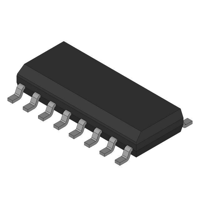
D OR N PACKAGE
(TOP VIEW)
High-Capacitance Loads at High Speeds
Output Supply Voltage Range From 5 V
to 24 V
Low Standby Power Dissipation
VCC3 Supply Maximizes Output Source
Voltage
VCC2
1Y
1A
1E1
1E2
2A
2Y
GND
description/ordering information
The SN75374 is a quadruple NAND interface
circuit designed to drive power MOSFETs from
TTL inputs. It provides the high current and
voltage necessary to drive large capacitive loads
at high speeds.
1
16
2
15
3
14
4
13
5
12
6
11
7
10
8
9
VCC1
4Y
4A
2E2
2E1
3A
3Y
VCC3
The outputs can be switched very close to the VCC2 supply rail when VCC3 is about 3 V higher than VCC2. VCC3
also can be tied directly to VCC2 when the source voltage requirements are lower.
ORDERING INFORMATION
PACKAGE†
TA
PDIP (N)
0°C
70°C
0
C to 70
C
SOIC (D)
ORDERABLE
PART NUMBER
Tube of 25
SN75374N
Tube of 40
SN75374D
Reel of 2500
SN75374DR
TOP-SIDE
MARKING
SN75374N
SN75374
† Package drawings, standard packing quantities, thermal data, symbolization, and PCB design
guidelines are available at www.ti.com/sc/package.
logic diagram (positive logic)
1E1
1E2
4
5
12
2E1
2E2
13
2
3
1A
7
2A
3A
6
10
11
15
4A
14
Please be aware that an important notice concerning availability, standard warranty, and use in critical applications of
Texas Instruments semiconductor products and disclaimers thereto appears at the end of this data sheet.
Copyright 2004, Texas Instruments Incorporated
���
������
� ����������� �� �!��"�� �� �� #!$%������� &��"'
���&!��� ������� �� �#"����������� #"� �(" �"��� �� �")�� �����!�"���
����&��& *������+' ���&!����� #���"����, &�"� ��� �"�"�����%+ ���%!&"
�"����, �� �%% #����"�"��'
POST OFFICE BOX 655303
• DALLAS, TEXAS 75265
1
��������
��
���
� ������
�����
SLRS028A − SEPTEMBER 1988 − REVISED NOVEMBER 2004
schematic (each driver)
VCC1
VCC3
VCC2
To Other Drivers
Input A
Enable E1
Output Y
Enable E2
GND
To Other Drivers
absolute maximum ratings over operating free-air temperature range (unless otherwise noted)†
Supply voltage range (see Note 1): VCC1 . . . . . . . . . . . . . . . . . . . . . . . . . . . . . . . . . . . . . . . . . . . . . . −0.5 V to 7 V
VCC2 . . . . . . . . . . . . . . . . . . . . . . . . . . . . . . . . . . . . . . . . . . . . . −0.5 V to 25 V
VCC3 . . . . . . . . . . . . . . . . . . . . . . . . . . . . . . . . . . . . . . . . . . . . . −0.5 V to 30 V
Input voltage, VI . . . . . . . . . . . . . . . . . . . . . . . . . . . . . . . . . . . . . . . . . . . . . . . . . . . . . . . . . . . . . . . . . . . . . . . . . . 5.5 V
Peak output current, II (tw < 10 ms, duty cycle < 50%) . . . . . . . . . . . . . . . . . . . . . . . . . . . . . . . . . . . . . . . 500 mA
Package thermal impedance, θJA (see Notes 2 and 3): D package . . . . . . . . . . . . . . . . . . . . . . . . . . . . 73°C/W
N package . . . . . . . . . . . . . . . . . . . . . . . . . . . . 67°C/W
Operating virtual junction temperature, TJ . . . . . . . . . . . . . . . . . . . . . . . . . . . . . . . . . . . . . . . . . . . . . . . . . . . 150°C
Storage temperature range, Tstg . . . . . . . . . . . . . . . . . . . . . . . . . . . . . . . . . . . . . . . . . . . . . . . . . . . −65°C to 150°C
† Stresses beyond those listed under “absolute maximum ratings” may cause permanent damage to the device. These are stress ratings only, and
functional operation of the device at these or any other conditions beyond those indicated under “recommended operating conditions” is not
implied. Exposure to absolute-maximum-rated conditions for extended periods may affect device reliability.
NOTES: 1. Voltage values are with respect to network ground terminal.
2. Maximum power dissipation is a function of TJ(max), θJA, and TA. The maximum allowable power dissipation at any allowable
ambient temperature is PD = (TJ(max) − TA)/θJA. Operating at the absolute maximum TJ of 150°C can affect reliability.
3. The package thermal impedance is calculated in accordance with JESD 51-7.
recommended operating conditions
VCC1
VCC2
MIN
NOM
MAX
UNIT
Supply voltage
4.75
5
5.25
V
Supply voltage
4.75
20
24
V
VCC2
0
24
28
V
4
10
V
VCC3
Supply voltage
VCC3 − VCC2 Voltage difference between supply voltages
2
VIH
VIL
High-level input voltage
2
Low-level input voltage
0.8
V
IOH
IOL
High-level output current
−10
mA
40
mA
TA
Operating free-air temperature
70
°C
Low-level output current
POST OFFICE BOX 655303
0
• DALLAS, TEXAS 75265
V
��������
��
���
� ������
�����
SLRS028A − SEPTEMBER 1988 − REVISED NOVEMBER 2004
electrical characteristics over recommended ranges of VCC1, VCC2, VCC3, and operating free-air
temperature (unless otherwise noted)
PARAMETER
VIK
VOH
TEST CONDITIONS
Input clamp voltage
II = − 12 mA
VCC3 = VCC2 + 3 V,
High-level output voltage
VCC3 = VCC2 + 3 V,
VCC3 = VCC2,
VCC3 = VCC2,
VIH = 2 V,
VIL = 0.8 V,
VIL = 0.8 V,
IOH = − 100 µA
IOH = − 10 mA
VIL = 0.8 V,
VIL = 0.8 V,
IOH = − 50 µA
IOH = − 10 mA
VCC2 = 15 V to 28 V,
IOL = 10 mA
VIH = 2 V,
Output clamp-diode
forward voltage
VI = 0,
IF = 20 mA
II
Input current at
maximum input voltage
VI = 5.5 V
High-level
input current
Any A
IIH
Low-level
input current
Any A
IIL
ICC1(H)
Supply current from
VCC1, all outputs high
ICC2(H)
Supply current from
VCC2, all outputs high
ICC3(H)
VOL
Low-level output voltage
VF
Any E
TYP†
MIN
MAX
UNIT
−1.5
V
VCC2 − 0.1
VCC2 − 0.3
VCC2 − 1.3 VCC2 − 0.9
VCC2 − 1 VCC2 − 0.7
V
VCC2 − 2.5 VCC2 − 1.8
0.15
0.3
0.25
0.5
IOL = 40 mA
1.5
1
40
VI = 2.4 V
80
−1
−1.6
−2
−3.2
4
8
−2.2
0.25
Supply current from
VCC3, all outputs high
2.2
3.5
ICC1(L)
Supply current from
VCC1, all outputs low
31
47
ICC2(L)
Supply current from
VCC2, all outputs low
ICC3(L)
Supply current from
VCC1, all outputs low
ICC2(H)
Supply current from
VCC2, all outputs high
ICC3(H)
Supply current from
Any E
VI = 0.4 V
VCC1 = 5.25 V,
All inputs at 0 V,
VCC1 = 5.25 V,
All inputs at 5 V,
VCC2 = 24 V,
No load
VCC2 = 24 V,
No load
VCC3 = 28 V,
VCC3 = 28 V,
2
16
Supply current from
VCC2, standby condition
ICC3(S)
Supply current from
VCC3, standby condition
V
mA
µA
A
mA
mA
mA
27
0.25
VCC1 = 5.25 V,
All inputs at 0 V,
VCC2 = 24 V,
No load
VCC3 = 24 V,
mA
0.5
VCC3, all outputs high
ICC2(S)
V
VCC1 = 0,
All inputs at 0 V,
VCC2 = 24 V,
No load
0.25
VCC3 = 24 V,
mA
0.5
† All typical values are at VCC1 = 5 V, VCC2 = 20 V, VCC3 = 24 V, and TA = 25°C, except for VOH for which VCC2 and VCC3 are as stated under test
conditions.
switching characteristics, VCC1 = 5 V, VCC2 = 20 V, VCC3 = 24 V, TA = 25°C
PARAMETER
TEST CONDITIONS
tDLH
tDHL
Delay time, low- to high-level output
tPLH
tPHL
Propagation delay time, low- to high-level output
tTLH
tTHL
MIN
Delay time, high- to low-level output
TYP
MAX
20
30
UNIT
ns
10
20
ns
10
40
60
ns
10
30
50
ns
Transition time, low- to high-level output
20
30
ns
Transition time, high- to low-level output
20
30
ns
Propagation delay time, high- to low-level output
POST OFFICE BOX 655303
CL = 200 pF,
RD = 24 Ω,
See Figure 1
• DALLAS, TEXAS 75265
3
��������
��
���
� ������
�����
SLRS028A − SEPTEMBER 1988 − REVISED NOVEMBER 2004
PARAMETER MEASUREMENT INFORMATION
5V
Input
24 V
20 V
VCC1 VCC2
VCC3
RD
Pulse
Generator
(see Note A)
Output
CL = 200 pF
(see Note B)
GND
2.4 V
TEST CIRCUIT
≤10 ns
≤10 ns
3V
90%
90%
Input
1.5 V
1.5 V
0.5 µs
t PHL
10%
t DHL
10%
0V
t PLH
t TLH
t THL
VCC2 − 2 V
VOH
VCC2 − 2 V
t DLH
Output
2V
2V
VOLTAGE WAVEFORMS
NOTES: A. The pulse generator has the following characteristics: PRR = 1 MHz, ZO ≈ 50 Ω .
B. CL includes probe and jig capacitance.
Figure 1. Test Circuit and Voltage Waveforms, Each Driver
4
POST OFFICE BOX 655303
• DALLAS, TEXAS 75265
VOL
��������
��
���
� ������
�����
SLRS028A − SEPTEMBER 1988 − REVISED NOVEMBER 2004
TYPICAL CHARACTERISTICS
HIGH-LEVEL OUTPUT VOLTAGE
vs
HIGH-LEVEL OUTPUT CURRENT
HIGH-LEVEL OUTPUT VOLTAGE
vs
HIGH-LEVEL OUTPUT CURRENT
VCC2
VOH
VOH − High-Level Output Voltage − V
VOH
VOH − High-Level Output Voltage − V
VCC2
− 0.5
TA = 70°C
−1
TA = 0°C
− 1.5
ÁÁ
ÁÁ
−2
−3
− 0.01
−0.5
−1
TA = 25°C
−1.5
ÁÁ
ÁÁ
VCC1 = 5 V
VCC2 = 20 V
VCC3 = 24 V
VI = 0.8 V
− 2.5
− 0.1
−1
− 10
VCC1 = 5 V
VCC2 = VCC3 = 20 V
V1 = 0.8 V
TA = 70°C
TA = 0°C
−2
−2.5
−3
−0.01
− 100
IOH − High-Level Output Current − mA
−0.1
Figure 2
−100
VOLTAGE TRANSFER CHARACTERISTICS
0.5
24
VCC1 = 5 V
VCC2 = 20 V
VCC3 = 24 V
VI = 2 V
0.4
20
− Output Voltage − V
VVO
O
VOL
VOL − Low-Level Output Voltage − V
−10
Figure 3
LOW-LEVEL OUTPUT VOLTAGE
vs
LOW-LEVEL OUTPUT CURRENT
ÁÁ
ÁÁ
ÁÁ
−1
IOH − High-Level Output Current − mA
TA = 70°C
0.3
TA = 0°C
16
12
ÁÁ
ÁÁ
0.2
0.1
0
8
VCC1 = 5 V
VCC2 = 20 V
VCC3 = 24 V
TA = 25°C
No Load
4
0
0
20
40
60
80
100
0
IOL − Low-Level Output Current − mA
Figure 4
0.5
1
1.5
2
VI − Input Voltage − V
2.5
Figure 5
POST OFFICE BOX 655303
• DALLAS, TEXAS 75265
5
��������
��
���
� ������
�����
SLRS028A − SEPTEMBER 1988 − REVISED NOVEMBER 2004
TYPICAL CHARACTERISTICS
PROPAGATION DELAY TIME
LOW- TO HIGH-LEVEL OUTPUT
vs
FREE-AIR TEMPERATURE
PROPAGATION DELAY TIME
HIGH- TO LOW-LEVEL OUTPUT
vs
FREE-AIR TEMPERATURE
250
250
VCC1 = 5 V
VCC2 = 20 V
VCC3 = 24 V
RD = 24 Ω
See Figure 1
200
175
CL = 4000 pF
225
ttPLH
PHL − Propagation Delay Time,
High− to Low−Level Output − ns
ttPLH
PLH − Propagation Delay Time,
Low- to High−Level Output − ns
225
CL = 2000 pF
150
125
100
CL = 1000 pF
75
50
CL = 200 pF
25
CL = 4000 pF
200
VCC1 = 5V
VCC2 = 20V
VCC3 = 24V
RD = 24 Ω
See Figure 1
175
150
CL = 2000 pF
125
100
CL = 1000 pF
75
50
CL = 200 pF
25
CL = 50 pF
0
CL = 50 pF
0
0
10
20
30
40
50
60
70
TA − Free-Air Temperature − °C
80
0
10
20
30
40
50
60
70
TA − Free-Air Temperature − °C
Figure 6
Figure 7
PROPAGATION DELAY TIME
LOW-TO HIGH-LEVEL OUTPUT
vs
VCC2 SUPPLY VOLTAGE
PROPAGATION DELAY TIME
HIGH- TO LOW-LEVEL OUTPUT
vs
VCC2 SUPPLY VOLTAGE
250
250
VCC1 = 5 V
VCC3 = VCC2 + 4 V
RD = 24 Ω
TA = 25°C
See Figure 1
200
VCC1 = 5 V
VCC3 = VCC2 + 4 V
RD = 24 Ω
TA = 25°C
See Figure 1
225
CL = 4000 pF
ttPLH
PHL − Propagation Delay Time,
High− to Low−Level Output − ns
ttPLH
PLH − Propagation Delay Time,
Low- to High−Level Output − ns
225
175
150
CL = 2000 pF
125
100
CL = 1000 pF
75
50
CL = 200 pF
CL = 50 pF
200
175
CL = 4000 pF
150
CL = 2000 pF
125
100
CL = 1000 pF
75
50
CL = 50 pF
25
CL = 200 pF
25
0
0
0
5
10
15
20
VCC2 − Supply Voltage − V
25
0
Figure 8
6
80
5
10
15
20
VCC2 − Supply Voltage − V
Figure 9
POST OFFICE BOX 655303
• DALLAS, TEXAS 75265
25
��������
��
���
� ������
�����
SLRS028A − SEPTEMBER 1988 − REVISED NOVEMBER 2004
TYPICAL CHARACTERISTICS
PROPAGATION DELAY TIME
LOW- TO HIGH-LEVEL OUTPUT
vs
LOAD CAPACITANCE
PROPAGATION DELAY TIME
HIGH- TO LOW-LEVEL OUTPUT
vs
LOAD CAPACITANCE
250
250
VCC1 = 5 V
VCC2 = 20 V
VCC3 = 24 V
TA = 25°C
See Figure 1
200
175
RD = 24 Ω
150
RD = 10 Ω
125
VCC1 = 5 V
VCC2 = 20 V
VCC3 = 24 V
TA = 25°C
See Figure 1
225
ttPLH
PHL − Propagation Delay Time,
High− to Low−Level Output − ns
ttPLH
PLH − Propagation Delay Time,
Low- to High−Level Output − ns
225
RD = 0
100
75
50
25
200
175
RD = 24 Ω
150
RD = 10 Ω
125
RD = 0
100
75
50
25
0
0
1000
2000
3000
0
4000
0
CL − Load Capacitance − pF
1000
2000
3000
4000
CL − Load Capacitance − pF
Figure 10
Figure 11
PT
PD − Power Dissipation − mW
POWER DISSIPATION (ALL DRIVERS)
vs
FREQUENCY
2000
1800
VCC1 = 5 V
VCC2 = 20 V
VCC3 = 24 V
Input: 3-V Square Wave
(50% duty cycle)
TA = 25°C
1600
CL = 600 pF
CL = 1000 pF
1400
1200
1000
CL = 2000 pF
800
600
CL = 4000 pF
400
CL = 400 pF
200
0
10
20
40
70 100
200
f − Frequency − kHz
400
1000
Figure 12
NOTE: For RD = 0, operation with CL > 2000 pF violates absolute maximum current rating.
POST OFFICE BOX 655303
• DALLAS, TEXAS 75265
7
��������
��
���
� ������
�����
SLRS028A − SEPTEMBER 1988 − REVISED NOVEMBER 2004
THERMAL INFORMATION
power-dissipation precautions
Significant power may be dissipated in the SN75374 driver when charging and discharging high-capacitance
loads over a wide voltage range at high frequencies. Figure 12 shows the power dissipated in a typical SN75374
as a function of frequency and load capacitance. Average power dissipated by this driver is derived from the
equation:
PT(AV) = PDC(AV) + PC(AV) + PS(AV)
where PDC(AV) is the steady-state power dissipation with the output high or low, PC(AV) is the power level during
charging or discharging of the load capacitance, and PS(AV) is the power dissipation during switching between
the low and high levels. None of these include energy transferred to the load, and all are averaged over a full
cycle.
The power components per driver channel are:
P DC(AV) +
( P H t H ) P Lt L)
T
f
P C(AV) [ CV 2c
P S(AV) +
(P LHt LH ) P HLt HL)
T
where the times are as defined in Figure 15.
t LH
t HL
tH
tL
T = 1/f
Figure 13. Output-Voltage Waveform
8
POST OFFICE BOX 655303
• DALLAS, TEXAS 75265
��������
��
���
� ������
�����
SLRS028A − SEPTEMBER 1988 − REVISED NOVEMBER 2004
THERMAL INFORMATION
power-dissipation precautions (continued)
PL, PH, PLH, and PHL are the respective instantaneous levels of power dissipation, and C is the load capacitance.
VC is the voltage across the load capacitance during the charge cycle shown by the equation:
VC = VOH − VOL
PS(AV) may be ignored for power calculations at low frequencies.
In the following power calculation, all four channels are operating under identical conditions: f = 0.2 MHz,
VOH = 19.9 V and VOL = 0.15 V with VCC1 = 5 V, VCC2 = 20 V, VCC3 = 24 V, VC = 19.75 V, C = 1000 pF, and the
duty cycle = 60%. At 0.2 MHz for CL < 2000 pF, PS(AV) is negligible and can be ignored. When the output voltage
is low, ICC2 is negligible and can be ignored.
On a per-channel basis using data-sheet values,
P DC(AV) +
Ǔ ) 20 Vǒ−2.24 mAǓ ) 24 Vǒ2.24mAǓƫ 0.6 )
ƪ5 Vǒ4 mA
4
Ǔ ) 24 Vǒ16 4mAǓƫ 0.4
ƪ5 Vǒ314mAǓ ) 20 Vǒ0 mA
4
PDC(AV) = 58.2 mW per channel
Power during the charging time of the load capacitance is
PC(AV) = (1000 pF)(19.75 V)2(0.2 MHz) = 78 mW per channel
Total power for each driver is:
PT(AV) = 58.2 mW + 78 mW = 136.2 mW
The total package power is:
PT(AV) = (136.2)(4) = 544.8 mW
POST OFFICE BOX 655303
• DALLAS, TEXAS 75265
9
��������
��
���
� ������
�����
SLRS028A − SEPTEMBER 1988 − REVISED NOVEMBER 2004
APPLICATION INFORMATION
driving power MOSFETs
The drive requirements of power MOSFETs are much lower than comparable bipolar power transistors. The
input impedance of an FET consists of a reverse-biased PN junction that can be described as a large
capacitance in parallel with a very high resistance. For this reason, the commonly used open-collector driver
with a pullup resistor is not satisfactory for high-speed applications. In Figure 14a, an IRF151 power MOSFET
switching an inductive load is driven by an open-collector transistor driver with a 470-Ω pullup resistor. The input
capacitance (CISS) specification for an IRF151 is 4000 pF maximum. The resulting long turn-on time, due to the
product of input capacitance and the pullup resistor, is shown in Figure 14b.
48 V
M
470 Ω
4
8
IRF151
7
3
TLC555
6
2
5
1/2
1
SN75447
VOH − VOL − Gate Voltage − V
5V
4
3
2
1
0
0
0.5
1
1.5
2
2.5
3
t − Time − µs
(a)
(b)
Figure 14. Power MOSFET Drive Using SN75447
A faster, more efficient drive circuit uses an active pullup, as well as an active pulldown output configuration,
referred to as a totem-pole output. The SN75374 driver provides the high-speed totem-pole drive desired in an
application of this type (see Figure 15a). The resulting faster switching speeds are shown in Figure 15b.
48 V
5V
4
8
7
6
TLC555
2
3
5
IRF151
1/4 SN75374
1
VOH − VOL − Gate Voltage − V
M
4
3
2
1
0
0
0.5
(a)
1.5
2
t − Time − µs
(b)
Figure 15. Power MOSFET Drive Using SN75374
10
1
POST OFFICE BOX 655303
• DALLAS, TEXAS 75265
2.5
3
��������
��
���
� ������
�����
SLRS028A − SEPTEMBER 1988 − REVISED NOVEMBER 2004
APPLICATION INFORMATION
driving power MOSFETs (continued)
Power MOSFET drivers must be capable of supplying high peak currents to achieve fast switching speeds as
shown by the equation:
I PK + VC
tr
where C is the capacitive load and tr is the desired rise time. V is the voltage that the capacitance is charged
to. In the circuit shown in Figure 14a, V is found by the equation:
V = VOH − VOL
Peak current required to maintain a rise time of 100 ns in the circuit of Figure 14a is:
I PK +
(3 * 0)4(10 −9)
+ 120 mA
100(10 −9)
Circuit capacitance can be ignored because it is very small compared to the input capacitance of the IRF151.
With a VCC of 5 V and assuming worst-case conditions, the gate drive voltage is 3 V.
For applications in which the full voltage of VCC2 must be supplied to the MOSFET gate, VCC3 should be at least
3 V higher than VCC2.
POST OFFICE BOX 655303
• DALLAS, TEXAS 75265
11
�PACKAGE OPTION ADDENDUM
www.ti.com
14-Oct-2022
PACKAGING INFORMATION
Orderable Device
Status
(1)
Package Type Package Pins Package
Drawing
Qty
Eco Plan
(2)
Lead finish/
Ball material
MSL Peak Temp
Op Temp (°C)
Device Marking
(3)
Samples
(4/5)
(6)
SN75374D
ACTIVE
SOIC
D
16
40
RoHS & Green
NIPDAU
Level-1-260C-UNLIM
0 to 70
SN75374
Samples
SN75374DE4
ACTIVE
SOIC
D
16
40
RoHS & Green
NIPDAU
Level-1-260C-UNLIM
0 to 70
SN75374
Samples
SN75374DR
ACTIVE
SOIC
D
16
2500
RoHS & Green
NIPDAU
Level-1-260C-UNLIM
0 to 70
SN75374
Samples
SN75374DRG4
ACTIVE
SOIC
D
16
2500
RoHS & Green
NIPDAU
Level-1-260C-UNLIM
0 to 70
SN75374
Samples
SN75374N
ACTIVE
PDIP
N
16
25
RoHS & Green
NIPDAU
N / A for Pkg Type
0 to 70
SN75374N
Samples
(1)
The marketing status values are defined as follows:
ACTIVE: Product device recommended for new designs.
LIFEBUY: TI has announced that the device will be discontinued, and a lifetime-buy period is in effect.
NRND: Not recommended for new designs. Device is in production to support existing customers, but TI does not recommend using this part in a new design.
PREVIEW: Device has been announced but is not in production. Samples may or may not be available.
OBSOLETE: TI has discontinued the production of the device.
(2)
RoHS: TI defines "RoHS" to mean semiconductor products that are compliant with the current EU RoHS requirements for all 10 RoHS substances, including the requirement that RoHS substance
do not exceed 0.1% by weight in homogeneous materials. Where designed to be soldered at high temperatures, "RoHS" products are suitable for use in specified lead-free processes. TI may
reference these types of products as "Pb-Free".
RoHS Exempt: TI defines "RoHS Exempt" to mean products that contain lead but are compliant with EU RoHS pursuant to a specific EU RoHS exemption.
Green: TI defines "Green" to mean the content of Chlorine (Cl) and Bromine (Br) based flame retardants meet JS709B low halogen requirements of