www.ti.com
SN75976A-EP
9-CHANNEL DIFFERENTIAL TRANSCEIVER
SLLS878A – JANUARY 2008 – REVISED FEBRUARY 2008
FEATURES
1
•
•
•
•
•
•
•
•
•
•
•
•
•
•
(1)
Controlled Baseline
– One Assembly Site
– One Test Site
– One Fabrication Site
Extended Temperature Performance of –55°C
to 125°C
Enhanced Diminishing Manufacturing Sources
(DMS) Support
Enhanced Product-Change Notification
Qualification Pedigree (1)
Designed to Operate at up to 20 Million Data
Transfers per Second (Fast-20 SCSI)
Nine Differential Channels for the Data and
Control Paths of the Small Computer Systems
Interface (SCSI) and Intelligent Peripheral
Interface (IPI)
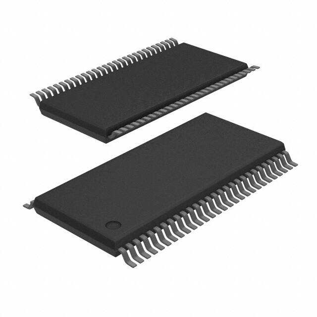
SN75976A Packaged in Thin Shrink
Small-Outline Package with 20-Mil Terminal
Pitch (DGG)
Two Skew Limits Available
ESD Protection on Bus Terminals Exceeds
12 kV
Low Disabled Supply Current 8 mA Typical
Thermal Shutdown Protection
Positive and Negative Current Limiting
Power-Up/Down Glitch Protection
Component qualification in accordance with JEDEC and
industry standards to ensure reliable operation over an
extended temperature range. This includes, but is not limited
to, Highly Accelerated Stress Test (HAST) or biased 85/85,
temperature cycle, autoclave or unbiased HAST,
electromigration, bond intermetallic life, and mold compound
life. Such qualification testing should not be viewed as
justifying use of this component beyond specified
performance and environmental limits.
DGG PACKAGE
(TOP VIEW)
GND
BSR
CRE
1A
1DE/RE
2A
2DE/RE
3A
3DE/RE
4A
4DE/RE
VCC
GND
GND
GND
GND
GND
VCC
5A
5DE/RE
6A
6DE/RE
7A
7DE/RE
8A
8DE/RE
9A
9DE/RE
1
56
2
55
3
54
4
53
5
52
6
51
7
50
8
49
9
48
10
47
11
46
12
45
13
44
14
43
15
42
16
41
17
40
18
39
19
38
20
37
21
36
22
35
23
34
24
33
25
32
26
31
27
30
28
29
CDE2
CDE1
CDE0
9B+
9B−
8B+
8B −
7B+
7B −
6B+
6B −
VCC
GND
GND
GND
GND
GND
VCC
5B+
5B −
4B+
4B −
3B+
3B −
2B+
2B −
1B+
1B −
Terminals 13 through 17 and 40 through 44 are connected together to the package lead frame
and signal ground.
DESCRIPTION/ORDERING INFORMATION
The SN75976A is an improved replacement for the industry's first 9-channel 485 transceiver – the SN75LBC976.
The A version offers improved switching performance, a smaller package, and higher ESD protection. The
SN75976A is offered in two versions. The '976A2 skew limits of 4 ns for the differential drivers and 5 ns for the
differential receivers complies with the recommended skew budget of the Fast-20 SCSI standard for data transfer
rates up to 20 million transfers per second. The '976A1 supports the Fast SCSI skew budget for 10 million
transfers per second. The skew limit ensures that the propagation delay times, not only from channel-to-channel
but from device-to-device, are closely matched for the tight skew budgets associated with high-speed parallel
data buses.
1
Please be aware that an important notice concerning availability, standard warranty, and use in critical applications of
Texas Instruments semiconductor products and disclaimers thereto appears at the end of this data sheet.
PRODUCTION DATA information is current as of publication date.
Products conform to specifications per the terms of the Texas
Instruments standard warranty. Production processing does not
necessarily include testing of all parameters.
Copyright © 2008, Texas Instruments Incorporated
�SN75976A-EP
9-CHANNEL DIFFERENTIAL TRANSCEIVER
www.ti.com
SLLS878A – JANUARY 2008 – REVISED FEBRUARY 2008
DESCRIPTION/ORDERING INFORMATION (CONTINUED)
The patented thermal enhancements made to the 56-pin shrink small-outline package (SSOP) of the SN75976
have been applied to the new, thin shrink, small-outline package (TSSOP). The TSSOP package offers even less
board area requirements than the SSOP while reducing the package height to 1 mm. This provides more board
area and allows component mounting to both sides of the printed circuit boards for low-profile, space-restricted
applications such as small form-factor hard disk drives.
In addition to speed improvements, the '976A can withstand electrostatic discharges exceeding 12 kV using the
human-body model, and 600 V using the machine model of MIL-PRF-38535, Method 3015.7 on the RS-485 I/O
terminals. This is six times the industry standard and provides protection from the noise that can be coupled into
external cables. The other terminals of the device can withstand discharges exceeding 4 kV and 400 V
respectively.
Each of the nine channels of the '976A typically meet or exceed the requirements of 485 (1983) and ISO
8482-1987/ TIA TR30.2 referenced by American National Standard of Information (ANSI) Systems, X3.131-1994
(SCSI-2) standard, X2.277-1996 (Fast-20 Parallel Interface), and the Intelligent Peripheral Interface Physical
Layer-ANSI X3.129-1986 standard.
The SN75976A is characterized for operation over an ambient air temperature range of –55°C to 125°C.
AVAILABLE OPTIONS (1)
SKEW LIMIT
(ns)
TA
–55°C to 125°C
(1)
(2)
(3)
2
PACKAGE (2) (3)
DRIVER
RECEIVER
TSSOP
(DGG)
8
9
SN75976A1MDGGREP
For the most current package and ordering information, see the Package Option Addendum at the end of this document, or see the TI
website at www.ti.com.
Package drawings, thermal data, and symbolization are available at www.ti.com/packaging.
The R suffix indicates taped and reeled packages.
Submit Documentation Feedback
Copyright © 2008, Texas Instruments Incorporated
Product Folder Link(s): SN75976A-EP
�SN75976A-EP
9-CHANNEL DIFFERENTIAL TRANSCEIVER
www.ti.com
SLLS878A – JANUARY 2008 – REVISED FEBRUARY 2008
TERMINAL FUNCTIONS
TERMINAL
NAME
NO.
LOGIC
LEVEL
I/O
TERMINATION
1A to 9A
4, 6, 8, 10,
19, 21, 23,
25, 27
TTL
I/O
Pullup
1B– to
9B–
29, 31, 33,
35, 37, 46,
48, 50, 52
RS-485
I/O
Pulldown
1B+ to
9B+
30, 32, 34,
36, 38, 47,
49, 51, 53
RS-485
I/O
Pullup
DESCRIPTION
1A to 9A carry data to and from the communication controller.
1B– to 9B– are the inverted data signals of the balanced pair to/from
the bus.
1B+ to 9B+ are the noninverted data signals of the balanced pair
to/from the bus.
BSR is the bit significant response. BSR disables receivers 1 through 8
and enables wired-OR drivers when BSR and DE/RE and CDE1 or
CDE2 are high. Channel 9 is placed in a high-impedance state with
BSR high.
BSR
2
TTL
Input
Pullup
CDE0
54
TTL
Input
Pulldown
CDE0 is the common driver enable 0. Its input signal enables all
drivers when CDE0 and 1DE/RE – 9DE/RE are high.
CDE1
55
TTL
Input
Pulldown
CDE1 is the common driver enable 1. Its input signal enables drivers1
to 4 when CDE1 is high and BSR is low.
CDE2
56
TTL
Input
Pulldown
CDE2 is the common driver enable 2. When CDE2 is high and BSR is
low, drivers 5 to 8 are enabled.
CRE
3
TTL
Input
Pullup
CRE is the common receiver enable. When high, CRE disables
receiver channels 5 to 9.
1DE/RE–9DE/RE are direction controls that transmit data to the bus
when it and CDE0 are high. Data is received from the bus when
1DE/RE–9DE/RE and CRE and BSR are low and CDE1 and CDE2 are
low.
1DE/RE to
9DE/RE
5, 7, 9, 11,
20, 22, 24,
26, 28
TTL
Input
Pullup
GND
1, 13, 14,
15, 16, 17,
40, 41, 42,
43, 44
NA
Power
NA
VCC
12, 18, 39,
45
NA
Power
NA
(1)
GND is the circuit ground. All GND terminals except terminal 1 are
physically tied to the die pad for improved thermal conductivity. (1)
Supply voltage
Terminal 1 must be connected to signal ground for proper operation.
Submit Documentation Feedback
Copyright © 2008, Texas Instruments Incorporated
Product Folder Link(s): SN75976A-EP
3
�SN75976A-EP
9-CHANNEL DIFFERENTIAL TRANSCEIVER
www.ti.com
SLLS878A – JANUARY 2008 – REVISED FEBRUARY 2008
LOGIC DIAGRAM (POSITIVE LOGIC)
CDE0
CDE1
BSR
1A
1DE/RE
2A
2DE/RE
3A
3DE/RE
4A
4DE/RE
CDE2
CRE
5A
5DE/RE
6A
6DE/RE
7A
7DE/RE
8A
8DE/RE
54
55
2
30
4
29
5
6
7
8
9
10
11
Channel 2
Channel 3
Channel 4
9DE/RE
4
32
31
34
33
36
35
2B+
2B−
3B+
3B−
4B+
4B−
56
3
38
19
37
5B+
5B−
20
21
22
23
24
25
26
Channel 6
Channel 7
Channel 8
2
9A
1B+
1B−
27
BSR
3
BSR
47
46
49
48
51
50
6B+
6B−
7B+
7B−
8B+
8B−
54
CRE
CDE0
53
9B+
52
9B−
28
Submit Documentation Feedback
Copyright © 2008, Texas Instruments Incorporated
Product Folder Link(s): SN75976A-EP
�SN75976A-EP
9-CHANNEL DIFFERENTIAL TRANSCEIVER
www.ti.com
SLLS878A – JANUARY 2008 – REVISED FEBRUARY 2008
SCHEMATICS OF INPUTS AND OUTPUTS
DE/RE, CRE, BSR, AND
A Inputs
CDE0, CDE1, AND CDE2 Inputs
VCC
VCC
100 kΩ
1 kΩ
1 kΩ
Input
Input
100 kΩ
8V
8V
B + Input
B − Input
VCC
100 kΩ
16 V
VCC
2 kΩ
2 kΩ
16 V
18 kΩ
Input
18 kΩ
Input
100 kΩ
4 kΩ
4 kΩ
16 V
16 V
B + AND B − Outputs
VCC
A Output
VCC
2 kΩ
16 V
18 kΩ
40 Ω
Output
Output
8V
4 kΩ
16 V
Submit Documentation Feedback
Copyright © 2008, Texas Instruments Incorporated
Product Folder Link(s): SN75976A-EP
5
�SN75976A-EP
9-CHANNEL DIFFERENTIAL TRANSCEIVER
www.ti.com
SLLS878A – JANUARY 2008 – REVISED FEBRUARY 2008
Absolute Maximum Ratings (1)
over operating free-air temperature range (unless otherwise noted)
VCC
IO
MIN
MAX
Supply voltage range (2)
–0.3
6
V
Bus voltage range
–10
15
V
Data I/O and control (A side) voltage range
–0.3
VCC + 0.5
Receiver output current
B side and GND, Class 3, A: (3)
Electrostatic discharge
Tstg
B side and GND, Class 3, B
(3)
(2)
(3)
(4)
V
±40
mA
12
kV
400
V
All terminals, Class 3, A:
4
kV
All terminals, Class 3, B:
400
V
150
°C
Storage temperature
–65
Continuous total power dissipation (4)
(1)
UNIT
Internally Limited
Stresses beyond those listed under "absolute maximum ratings" may cause permanent damage to the device. These are stress ratings
only, and functional operation of the device at these or any other conditions beyond those indicated under "recommended operating
conditions" is not implied. Exposure to absolute-maximum-rated conditions for extended periods may affect device reliability.
All voltage values are with respect to the GND terminals.
This absolute maximum rating is tested in accordance with MIL-STD-883, Method 3015.7.
The maximum operating junction temperature is internally limited. Use the Dissipation Rating Table to operate below this temperature.
Dissipation Ratings
(1)
PACKAGE
TA ≤ 25°C
OPERATING FACTOR (1)
ABOVE TA = 25°C
TA = 70°C
POWER RATING
TA = 125°C
POWER RATING
DGG
2500 mW
20 mW/°C
1600 mW
–
This is the inverse of the junction-to-ambient thermal resistance when board-mounted and with no air flow.
Package Thermal Characteristics
PARAMETER
TEST CONDITIONS
MIN
TYP
MAX
UNIT
RqθJA
Junction-to-ambient thermal resistance
DGG, board-mounted, no air flow
50
°C/W
RθJC
Junction-to-case thermal resistance
DGG
27
°C/W
TJS
Thermal-shutdown junction temperature
165
°C
6
Submit Documentation Feedback
Copyright © 2008, Texas Instruments Incorporated
Product Folder Link(s): SN75976A-EP
�SN75976A-EP
9-CHANNEL DIFFERENTIAL TRANSCEIVER
www.ti.com
SLLS878A – JANUARY 2008 – REVISED FEBRUARY 2008
1000.00
Electromigration Fail Mode
Years estimated life
100.00
Wirebond Voiding
Fail Mode
10.00
1.00
0.10
100
110
120
130
140
150
160
Continuous Tj (°C)
A.
See Datasheet for Absolute Maximum and Minimum Recommended Operating Conditions.
B.
Silicon Operating ife Design Goal is 10 years @105°C Junction Temperature (does not include package interconnect
life).
C.
Enhanced Plastic Product Disclaimer Applies.
D.
Long-term high-temperature storage and/or extended use at maximum recommended operating conditions may result
in a reduction of overall device life. See Chart for additional information on thermal derating. Electromigration failure
mode applies to powered part, Kirkendall voiding failure mode is a function of temperature only.
Figure 1. SN75976A-EP Operating Life Derating Chart
Recommended Operating Conditions
VCC
Supply voltage
VIH
High-level input voltage
Except nB+, nB– (1)
VIL
Low-level input voltage
Except nB+, nB– (1)
VO, VI,
or VIC
Voltage at any bus terminal (separately or common-mode)
nB+ or nB–
IOH
High-level output current
IOL
Low-level output current
TA
Operating free-air temperature
(1)
MIN
NOM
MAX
UNIT
4.75
5
5.25
V
2
V
0.8
12
–7
Driver
–60
Receiver
–8
Driver
60
Receiver
SN75976A
8
–55
125
V
V
mA
mA
°C
n=1–9
Submit Documentation Feedback
Copyright © 2008, Texas Instruments Incorporated
Product Folder Link(s): SN75976A-EP
7
�SN75976A-EP
9-CHANNEL DIFFERENTIAL TRANSCEIVER
www.ti.com
SLLS878A – JANUARY 2008 – REVISED FEBRUARY 2008
Electrical Characteristics
over recommended operating free-air temperature range (unless otherwise noted)
PARAMETER
VODH
VODL
VOH
Driver differential high-level output
voltage
TEST CONDITIONS
S1 to A,
High-level output voltage
0.7
S1 to B,
See Figure 1
VT = 5 V,
0.7
S1 to A,
TC ≥ 25°C
VT = 5 V,
See Figure 2
0.7
–1.4
See Figure 2
0.7
–1.8
–0.8
–1.4
4
4.5
Low-level output voltage
VT = 5 V,
S1 to A,
See Figure 1
VT = 5 V,
A side,
IOH = –8 mA
VID = 200 mV,
See Figure 4
B side,
VOL
TYP (1)
See Figure 2
Driver differential low-level output voltage S1 to B,
VT = 5 V,
MIN
VT = 5 V,
A side,
IOH = 8 mA
A side,
See Figure 2
UNIT
V
V
V
3
VID = –200 mV,
See Figure 4
VT = 5 V,
MAX
0.6
See Figure 2
0.8
V
1
VIT+
Receiver positive-going differential input
threshold voltage
IOH = –8 mA,
See Figure 4
0.2
V
VIT–
Receiver negative-going differential input
threshold voltage
IOL = 8 mA,
See Figure 4
–0.2
V
Vhys
Receiver input hysteresis
(VIT+ – VIT–)
VCC = 5 V,
TA = 25°C
II
Bus input current
IIH
High-level input current
IIL
Low-level input current
IOS
Short circuit output current
IOZ
High-impedance-state output current
ICC
Supply current
CO
Output capacitance
24
45
VIH = 12 V,
VCC = 5 V,
Other input at 0 V
0.4
VIH = 12 V,
VCC = 0,
Other input at 0 V
0.5
1
VIH = –7 V,
VCC = 5 V,
Other input at 0 V
–0.4
–0.8
VIH = –7 V,
Power dissipation capacitance (2)
(1)
(2)
1
VCC = 0,
Other input at 0 V
–0.3
VIH = 2 V
–100
CDE0, CDE1, and CDE2,
VIH = 2V
100
A, BSR, DE/RE, and CRE,
VIL = 0.8 V
–100
CDE1, CDE1, and CDE2,
VIL = 0.8 V
100
nB+ or nB–
±260
A
mA
–0.8
A, BSR, DE/RE, and CRE,
µA
µA
mA
See IIH and IIL
nB+ or nB–
See II
Disabled
10
All drivers enabled, no load
60
All receivers enabled, no load
Cpd
mV
mA
45
nB+ or nB– to GND
18
Receiver
40
Driver
pF
pF
100
All typical values are at VCC = 5 V, TA = 25°C.
Cpd determines the no-load dynamic supply current consumption, IS = CPD × VCC × f + ICC.
Driver Switching Characteristics
over recommended operating conditions (unless otherwise noted)
PARAMETER
TEST CONDITIONS
tpd
Propagation delay time, tPHL or tPLH
(see Figures 2 and 3)
'976A1
tsk(lim)
Skew limit, maximum tpd – minimum tpd (2)
'976A1
tsk(p)
Pulse skew, |tPHL – tPLH|
(1)
(2)
8
VCC = 5 V,
MIN
TA = 25°C
TYP (1)
MAX
UNIT
15
ns
8
ns
4
ns
All typical values are at VCC = 5 V, TA = 25°C.
This parameter is applicable at one VCC and operating temperature within the recommended operating conditions and to any two
devices.
Submit Documentation Feedback
Copyright © 2008, Texas Instruments Incorporated
Product Folder Link(s): SN75976A-EP
�SN75976A-EP
9-CHANNEL DIFFERENTIAL TRANSCEIVER
www.ti.com
SLLS878A – JANUARY 2008 – REVISED FEBRUARY 2008
Driver Switching Characteristics (continued)
over recommended operating conditions (unless otherwise noted)
PARAMETER
TEST CONDITIONS
tf
Fall time
S1 to B,
tr
Rise time
See Figure 3
ten
Enable time, control inputs to active output
tdis
MIN
See Figure 3
TYP (1)
MAX
4
UNIT
ns
8
ns
60
ns
Disable time, control inputs to high-impedance output
140
ns
tPHZ
Propagation delay time, high-level to high-impedance
output
120
ns
tPLZ
Propagation delay time, low-level to high-impedance
output
120
ns
60
ns
60
ns
tPZH
Propagation delay time, high-impedance to high-level
output
tPZL
Propagation delay time, high-impedance to low-level
output
See Figures 6 and 7
Receiver Switching Characteristics
over recommended operating conditions (unless otherwise noted)
PARAMETER
TEST CONDITIONS
MIN
TYP (1)
MAX
UNIT
tpd
Propagation delay time, tPHL or tPLH
(see Figures 4 and 5)
'976A1
tsk(lim)
Skew limit, maximum tpd – minimum tpd (2)
'976A1
tsk(p)
Pulse skew, |tPHL – tPLH|
tt
Transition time (tr or tf)
ten
Enable time, control inputs to active output
70
ns
tdis
Disable time, control inputs to high-impedance output
80
ns
tPHZ
Propagation delay time, high-level to high-impedance
output
80
ns
tPLZ
Propagation delay time, low-level to high-impedance
output
70
ns
70
ns
70
ns
TA = 25°C
0.6
See Figure 5
tPZH
Propagation delay time, high-impedance to high-level
output
tPZL
Propagation delay time, high-impedance to low-level
output
(1)
(2)
VCC = 5 V,
19
ns
9
ns
4
ns
2
ns
See Figures 8 and 9
All typical values are at VCC = 5 V, TA = 25°C.
This parameter is applicable at one VCC and operating temperature within the recommended operating conditions and to any two
devices.
Submit Documentation Feedback
Copyright © 2008, Texas Instruments Incorporated
Product Folder Link(s): SN75976A-EP
9
�SN75976A-EP
9-CHANNEL DIFFERENTIAL TRANSCEIVER
www.ti.com
SLLS878A – JANUARY 2008 – REVISED FEBRUARY 2008
PARAMETER MEASUREMENT INFORMATION
SN75976A = 5 V
SN55976A = 4.5 V
A
S1
B+
IO
15 pF
II
Input
(see Note A)
A
165 Ω
B
165 Ω
375 Ω
VO
VI
375 Ω
75 Ω
VOD
IO
B−
†
‡
S2
VO
†
15 pF
CDE0 and DE/RE are at 2 V, BSR is at 0.8 V and, for the SN75976A only, all others are open.
For the SN75976A only, all nine drivers are enabled, similarly loaded, and switching.
A.
All input pulses are supplied by a generator having the following characteristics: tr ≤ 6 ns, tf ≤ 6 ns, PRR ≤ 1 MHz,
duty cycle = 50%, ZO = 50 Ω.
B.
All resistances are in Ω and ± 5%, unless otherwise indicated.
C.
All capacitances are in pF and ± 10%, unless otherwise indicated.
D.
All indicated voltages are ± 10 mV.
Figure 2. Driver Test Circuit, Currents, and Voltages
3V
Input
1.5 V
1.5 V
0V
tPLH
Output, VOD
tPHL
0V
10%
90%
tr
90%
VOD(H)
0V
10%
S1 to A or B
VOD(L)
tf
A.
All input pulses are supplied by a generator having the following characteristics: tr ≤ 6 ns, tf ≤ 6 ns, PRR ≤ 1 MHz,
duty cycle = 50%, ZO = 50 Ω.
B.
All resistances are in Ω and ± 5%, unless otherwise indicated.
C.
All capacitances are in pF and ± 10%, unless otherwise indicated.
D.
All indicated voltages are ± 10 mV.
Figure 3. Driver Delay and Transition Time Test Waveforms
10
Submit Documentation Feedback
Copyright © 2008, Texas Instruments Incorporated
Product Folder Link(s): SN75976A-EP
�SN75976A-EP
9-CHANNEL DIFFERENTIAL TRANSCEIVER
www.ti.com
SLLS878A – JANUARY 2008 – REVISED FEBRUARY 2008
PARAMETER MEASUREMENT INFORMATION (continued)
Generator
(see Note A)
Input B +
50 Ω
IO
VID
Generator
(see Note A)
50 Ω
Output
Input B −
VO
CL = 15 pF
†
†
‡
CDE0, CDE1, CDE2, BSR, CRE, and DE/RE at 0.8 V
For the SN75976A only, all nine receivers are enabled and switching.
A.
All input pulses are supplied by a generator having the following characteristics: tr ≤ 6 ns, tf ≤ 6 ns, PRR ≤ 1 MHz,
duty cycle = 50%, ZO = 50 Ω.
B.
All resistances are in Ω and ± 5%, unless otherwise indicated.
C.
All capacitances are in pF and ± 10%, unless otherwise indicated.
D.
All indicated voltages are ± 10 mV.
Figure 4. Receiver Propagation Delay and Transition Time Test Circuit
3V
Input B −
1.5 V
1.5 V
Input B +
0V
tPLH
Output
tPHL
1.4 V
10%
90%
tr
90%
VOH
1.4 V
10%
VOL
tf
A.
All input pulses are supplied by a generator having the following characteristics: tr ≤ 6 ns, tf ≤ 6 ns, PRR ≤ 1 MHz,
duty cycle = 50%, ZO = 50 Ω.
B.
All resistances are in Ω and ± 5%, unless otherwise indicated.
C.
All capacitances are in pF and ± 10%, unless otherwise indicated.
D.
All indicated voltages are ± 10 mV.
Figure 5. Receiver Delay and Transition Time Waveforms
Submit Documentation Feedback
Copyright © 2008, Texas Instruments Incorporated
Product Folder Link(s): SN75976A-EP
11
�SN75976A-EP
9-CHANNEL DIFFERENTIAL TRANSCEIVER
www.ti.com
SLLS878A – JANUARY 2008 – REVISED FEBRUARY 2008
PARAMETER MEASUREMENT INFORMATION (continued)
4.5 V
A
S1
B+
50 pF
A
0 V or 3 V
165 Ω
B
165 Ω
375 Ω
75 Ω
VOD
375 Ω
B−
DE/RE
S2
50 pF†
See Table 1
Input
†
Includes probe and jig capacitance in two places.
A.
All input pulses are supplied by a generator having the following characteristics: tr ≤ 6 ns, tf ≤ 6 ns, PRR ≤ 1 MHz,
duty cycle = 50%, ZO = 50 Ω.
B.
All resistances are in Ω and ± 5%, unless otherwise indicated.
C.
All capacitances are in pF and ± 10%, unless otherwise indicated.
D.
All indicated voltages are ± 10 mV.
Figure 6. Driver Enable and Disable Time Test Circuit
Table 1. Enabling For Driver Enable and Disable Time
DRIVER
BSR
CDE0
CDE1
CDE2
CRE
1–8
H
H
L
L
X
9
L
H
H
H
H
3V
Input, DE/RE
1.5 V
1.5 V
0V
tPZH
tPHZ
VOD(H)
Output, VOD
0V
0V
∼ −1 V
tPZL
A at 3V
S1 to B
tPLZ
∼1V
Output, VOD
0V
0V
VOD(L)
A at 0V
S1 to A
A.
All input pulses are supplied by a generator having the following characteristics: tr ≤ 6 ns, tf ≤ 6 ns, PRR ≤ 1 MHz,
duty cycle = 50%, ZO = 50 Ω.
B.
All resistances are in Ω and ± 5%, unless otherwise indicated.
C.
All capacitances are in pF and ± 10%, unless otherwise indicated.
D.
All indicated voltages are ± 10 mV.
Figure 7. Driver Enable Time Waveforms
12
Submit Documentation Feedback
Copyright © 2008, Texas Instruments Incorporated
Product Folder Link(s): SN75976A-EP
�SN75976A-EP
9-CHANNEL DIFFERENTIAL TRANSCEIVER
www.ti.com
SLLS878A – JANUARY 2008 – REVISED FEBRUARY 2008
VT
620 Ω
B+
0 V or 3 V
A
Output
DE/RE
Input
3 V or 0 V
†
40 pF‡
B−
†
CDE0 is high, CDE1, CDE2, BSR, and CRE are low and, for
the SN75976A only, all others are open.
‡ Includes probe and jig capacitance.
A.
All input pulses are supplied by a generator having the following characteristics: tr ≤ 6 ns, tf ≤ 6 ns, PRR ≤ 1 MHz,
duty cycle = 50%, ZO = 50 Ω.
B.
All resistances are in Ω and ± 5%, unless otherwise indicated.
C.
All capacitances are in pF and ± 10%, unless otherwise indicated.
D.
All indicated voltages are ± 10 mV.
Figure 8. Receiver Enable and Disable Time Test Circuit
3V
Input
1.4 V
1.4 V
0V
tPLZ
tPZL
1.4 V
Output
VOD
1.4 V
B + at 0 V
B − at 3 V
VT = VCC
Indeterminate
tPZH
tPHZ
1.4 V
Output
1.4 V
B + at 3 V
B − at 0 V
VT = 0
Indeterminate
VOD
A.
All input pulses are supplied by a generator having the following characteristics: tr ≤ 6 ns, tf ≤ 6 ns, PRR ≤ 1 MHz,
duty cycle = 50%, ZO = 50 Ω.
B.
All resistances are in Ω and ± 5%, unless otherwise indicated.
C.
All capacitances are in pF and ± 10%, unless otherwise indicated.
D.
All indicated voltages are ± 10 mV.
Figure 9. Receiver Enable and Disable Time Waveforms
Submit Documentation Feedback
Copyright © 2008, Texas Instruments Incorporated
Product Folder Link(s): SN75976A-EP
13
�SN75976A-EP
9-CHANNEL DIFFERENTIAL TRANSCEIVER
www.ti.com
SLLS878A – JANUARY 2008 – REVISED FEBRUARY 2008
TYPICAL CHARACTERISTICS
LOGIC INPUT CURRENT
vs
INPUT VOLTAGE
AVERAGE SUPPLY CURRENT
vs
FREQUENCY
−30
A, DE/RE,CRE,BSR
−25
200
I I − Logic Input Current − µ A
I CC − Average Supply Current − mA
250
150
ÁÁ
ÁÁ
ÁÁ
ÁÁ
100
9 Drivers
50
−20
−15
−10
−5
9 Receivers
0
0.001
0
0.01
0.1
1
10
100
0
1
f − Frequency − MHz
2
3
VI − Input Voltage − V
Figure 10.
BUS
LOW-LEVEL OUTPUT VOLTAGE
vs
LOW-LEVEL OUTPUT CURRENT
15
VOL − Low-Level Output Voltage − V
2.5
I I − Input Current − mA
10
5
ÁÁ
ÁÁ
ÁÁ
ÁÁ
0
−5
2
1.5
1
0.5
0
−15
−10
−5
0
5
10
15
20
0
10
VI − Input Voltage − V
Figure 12.
14
5
Figure 11.
DRIVER
INPUT CURRENT
vs
INPUT VOLTAGE
−10
−20
4
Submit Documentation Feedback
20
30
40
50
60
70
80
90 100
IOL − Low-Level Output Current − mA
Figure 13.
Copyright © 2008, Texas Instruments Incorporated
Product Folder Link(s): SN75976A-EP
�SN75976A-EP
9-CHANNEL DIFFERENTIAL TRANSCEIVER
www.ti.com
SLLS878A – JANUARY 2008 – REVISED FEBRUARY 2008
TYPICAL CHARACTERISTICS (continued)
DRIVER
DRIVER
HIGH-LEVEL OUTPUT VOLTAGE
vs
HIGH-LEVEL OUTPUT CURRENT
AVERAGE DIFFERENTIAL OUTPUT VOLTAGE
vs
AVERAGE CASE TEMPERATURE
4
|VOD | − Average Differential Output Voltage − V
2.5
VOH − High-Level Output Voltage − V
3.5
ÁÁ
ÁÁ
ÁÁ
ÁÁ
3
2.5
2
ÁÁ
ÁÁ
ÁÁ
ÁÁ
1.5
1
0.5
0
0
−20
−40
−60
−80
IOH − High-Level Output Current − mA
Figure 14.
RECEIVER
VOD(L), VCC = 5.25 V
2
1.5
VOD(L), VCC = 4.75 V
1
VOD(H), VCC = 5.25 V
VOD(H), VCC = 4.75 V
0.5
S1 to Position B (see Figure 1)
0
0
−100
20
40
60
80
100
120
TC − Average Case Temperature − °C
140
Figure 15.
DRIVER
PROPAGATION DELAY TIME
vs
CASE TEMPERATURE
PROPAGATION DELAY TIME
vs
CASE TEMPERATURE
16
14
VCC = 5 V,
S1 to Position B (see Figure 1)
tPHL(max)
12
t pd − Propagation Delay Time − ns
t pd − Propagation Delay Time − ns
14
tPLH(max)
tPHL(min)
10
tPLH(min)
8
6
(Data Extracted From 7 Wafer Lots)
4
12
tPHL(max)
10
8
tPLH(max)
6
tPLH(min)
tPHL(min)
4
2
VCC = 5 V
Data Extracted From 7 Wafer Lots
2
0
0
20
40
60
80
100
120
140
0
TC − Case Temperature − °C
Figure 16.
20
40
60
80
100
120
Submit Documentation Feedback
Copyright © 2008, Texas Instruments Incorporated
Product Folder Link(s): SN75976A-EP
140
TC − Case Temperature − °C
Figure 17.
15
�SN75976A-EP
9-CHANNEL DIFFERENTIAL TRANSCEIVER
www.ti.com
SLLS878A – JANUARY 2008 – REVISED FEBRUARY 2008
TYPICAL CHARACTERISTICS (continued)
DRIVER
OUTPUT CURRENT
vs
SUPPLY VOLTAGE
100
TA = 25°C
80
I O − Output Current − mA
IOH
60
40
20
0
−20
−40
−60
IOL
−80
0
1
2
3
4
VCC − Supply Voltage − V
5
6
Figure 18.
16
Submit Documentation Feedback
Copyright © 2008, Texas Instruments Incorporated
Product Folder Link(s): SN75976A-EP
�SN75976A-EP
9-CHANNEL DIFFERENTIAL TRANSCEIVER
www.ti.com
SLLS878A – JANUARY 2008 – REVISED FEBRUARY 2008
APPLICATION INFORMATION
Table 2. Typical Signal and Terminal Assignments (1) (2)
SIGNAL
TERMINAL
SCSI DATA
SCSI CONTROL
IPI DATA
IPI CONTROL
CDE0
54
DIFFSENSE
DIFFSENSE
VCC
VCC
CDE1
55
GND
GND
XMTA, XMTB
GND
CDE2
56
GND
GND
XMTA, XMTB
SLAVE/MASTER
BSR
2
GND
GND
GND, BSR
GND
CRE
3
GND
GND
GND
VCC
1A
4
DB0, DB8
ATN
AD7, BD7
NOT USED
1DE/RE
5
DBE0, DBE8
INIT EN
GND
GND
2A
6
DB1, DB9
BSY
AD6, BD6
NOT USED
2DE/RE
7
DBE1, DBE9
BSY EN
GND
GND
3A
8
DB2, DB10
ACK
AD5, BD5
SYNC IN
3DE/RE
9
DBE2, DBE10
INIT EN
GND
GND
4A
10
DB3, DB11
RST
AD4, BD4
SLAVE IN
4DE/RE
11
DBE3, DBE11
GND
GND
GND
5A
19
DB4, DB12
MSG
AD3, BD3
NOT USED
5DE/RE
20
DBE4, DBE12
TARG EN
GND
GND
6A
21
DB5, DB13
SEL
AD2, BD2
SYNC OUT
6DE/RE
22
DBE5, DBE13
SEL EN
GND
GND
7A
23
DB6, DB14
C/D
AD1, BD1
MASTER OUT
7DE/RE
24
DBE6, DBE14
TARG EN
GND
GND
8A
25
DB7, DB15
REQ
AD0, BD0
SELECT OUT
8DE/RE
26
DBE7, DBE15
TARG EN
GND
GND
9A
27
DBP0, DBP1
I/O
AP, BP
ATTENTION IN
9DE/RE
28
DBPE0, DBPE1
TARG EN
XMTA, XMTB
VCC
(1)
(2)
ABBREVIATIONS:
DBn = data bit n, where n = (0, 1, . . . , 15)
DBEn = data bit n enable, where n = (0, 1, . . . , 15)
DBP0 = parity bit for data bits 0 through 7 or IPI bus A
DBPE0 = parity bit enable for P0
DBP1 = parity bit for data bits 8 through 15 or IPI bus B
DBPE1 = parity bit enable for P1
ADn or BDn = IPI Bus A – Bit n (ADn) or Bus B – Bit n (BDn), where n = (0, 1, . . . , 7)
AP or BP = IPI parity bit for bus A or bus B
XMTA or XMTB = transmit enable for IPI bus A or B
BSR = bit significant response
INIT EN = common enable for SCSI initiator mode
TARG EN = common enable for SCSI target mode
Signal inputs are shown as active high. When only active-low inputs are available, logic inversion is accomplished by reversing the B+
and B– connector terminal assignments.
Submit Documentation Feedback
Copyright © 2008, Texas Instruments Incorporated
Product Folder Link(s): SN75976A-EP
17
�SN75976A-EP
9-CHANNEL DIFFERENTIAL TRANSCEIVER
www.ti.com
SLLS878A – JANUARY 2008 – REVISED FEBRUARY 2008
Function Tables
RECEIVER
DRIVER
B+
A
INPUTS
B+
A
B−
B−
B +(B)
B −(B)
OUTPUT
A
INPUT
A
L
H
H
L
L
H
L
H
TRANSCEIVER
OUTPUTS
B+
B−
L
H
H
L
DRIVER WITH ENABLE
B+
A
B+
B−
A
B−
DE/RE
DE/RE
DE/RE
L
L
H
H
INPUTS
A B +(B) B −(B)
−
−
L
H
L
H
−
−
H
L
−
−
A
INPUTS
DE/RE
A
OUTPUTS
B−
B+
L
H
−
−
−
−
L
H
L
L
H
H
−
−
H
L
WIRED-OR DRIVER
L
H
L
H
OUTPUTS
B−
B+
Z
Z
L
H
Z
Z
H
L
TWO-ENABLE INPUT DRIVER
B+
A
A
B−
B+
B−
DE/RE
INPUT
A
L
H
18
OUTPUTS
B+
B−
Z
H
Z
L
INPUTS
DE/RE A
L
L
H
H
L
H
L
H
OUTPUTS
B−
B+
Z
H
L
H
Z
L
H
L
A.
H = high level, L = low level, X = irrelevant, Z = high impedance (off)
B.
An H in this column represents a voltage of 200 mV or higher than the other bus input. An L represents a voltage of
200 mV or lower than the other bus input. Any voltage less than 200 mV results in an indeterminate receiver output.
Submit Documentation Feedback
Copyright © 2008, Texas Instruments Incorporated
Product Folder Link(s): SN75976A-EP
�SN75976A-EP
9-CHANNEL DIFFERENTIAL TRANSCEIVER
www.ti.com
SLLS878A – JANUARY 2008 – REVISED FEBRUARY 2008
A.
When 0 is open drain
B.
Must be open-drain or 3-state output
C.
The BSR, CRE, A, and DE/RE inputs have internal pullup resistors. CDE0, CDE1, and CDE2 have internal pulldown
resistors.
Figure 19. Typical SCSI Transceiver Connections
Submit Documentation Feedback
Copyright © 2008, Texas Instruments Incorporated
Product Folder Link(s): SN75976A-EP
19
�SN75976A-EP
9-CHANNEL DIFFERENTIAL TRANSCEIVER
www.ti.com
SLLS878A – JANUARY 2008 – REVISED FEBRUARY 2008
Channel Logic Configurations With Control Input Logic
The following logic diagrams show the positive-logic representation for all combinations of control inputs. The
control inputs are from MSB to LSB; the BSR, CDE0, CDE1, CDE2, and CRE bit values are shown below the
diagrams. Channel 1 is at the top of the logic diagrams; channel 9 is at the bottom of the logic diagrams.
Hi-Z
Hi-Z
Hi-Z
Hi-Z
Hi-Z
Figure 20. 00000
20
Hi-Z
Figure 21. 00001
Figure 22. 00010
Figure 23. 00011
Submit Documentation Feedback
Figure 24. 00100
Copyright © 2008, Texas Instruments Incorporated
Product Folder Link(s): SN75976A-EP
�SN75976A-EP
9-CHANNEL DIFFERENTIAL TRANSCEIVER
www.ti.com
SLLS878A – JANUARY 2008 – REVISED FEBRUARY 2008
Hi-Z
Hi-Z
Hi-Z
Hi-Z
Hi-Z
Hi-Z
Figure 25. 00101
Figure 26. 00110
Figure 27. 00111
Figure 29. 01001
Figure 28. 01000
Submit Documentation Feedback
Copyright © 2008, Texas Instruments Incorporated
Product Folder Link(s): SN75976A-EP
21
�SN75976A-EP
9-CHANNEL DIFFERENTIAL TRANSCEIVER
www.ti.com
SLLS878A – JANUARY 2008 – REVISED FEBRUARY 2008
Figure 34. 01110
Figure 33. 01101
Figure 31. 01011
Figure 30. 01010
22
Figure 32. 01100
Submit Documentation Feedback
Copyright © 2008, Texas Instruments Incorporated
Product Folder Link(s): SN75976A-EP
�SN75976A-EP
9-CHANNEL DIFFERENTIAL TRANSCEIVER
www.ti.com
SLLS878A – JANUARY 2008 – REVISED FEBRUARY 2008
Hi-Z
Hi-Z
Hi-Z
Hi-Z
Hi-Z
Hi-Z
Hi-Z
Hi-Z
Hi-Z
Hi-Z
Hi-Z
Hi-Z
Hi-Z
Figure 35. 01111
Figure 36. 10000
and 10001
Hi-Z
Hi-Z
Hi-Z
Hi-Z
Hi-Z
Hi-Z
Figure 37. 10010
and 10011
Figure 38. 10100
and 10101
Hi-Z
Figure 39. 10110
and 10111
Submit Documentation Feedback
Copyright © 2008, Texas Instruments Incorporated
Product Folder Link(s): SN75976A-EP
23
�SN75976A-EP
9-CHANNEL DIFFERENTIAL TRANSCEIVER
www.ti.com
SLLS878A – JANUARY 2008 – REVISED FEBRUARY 2008
Hi-Z
Figure 40. 11000 and
11001
Hi-Z
Figure 41. 11010 and
11011
Hi-Z
Figure 42. 11100 and
11101
Hi-Z
Figure 43. 11110 and
11111
24
Submit Documentation Feedback
Copyright © 2008, Texas Instruments Incorporated
Product Folder Link(s): SN75976A-EP
�PACKAGE OPTION ADDENDUM
www.ti.com
10-Dec-2020
PACKAGING INFORMATION
Orderable Device
Status
(1)
Package Type Package Pins Package
Drawing
Qty
Eco Plan
(2)
Lead finish/
Ball material
MSL Peak Temp
Op Temp (°C)
Device Marking
(3)
(4/5)
(6)
SN75976A1MDGGREP
ACTIVE
TSSOP
DGG
56
2000
RoHS & Green
NIPDAU
Level-2-260C-1 YEAR
-55 to 125
2E976A1EP
V62/08614-01XE
ACTIVE
TSSOP
DGG
56
2000
RoHS & Green
NIPDAU
Level-2-260C-1 YEAR
-55 to 125
2E976A1EP
(1)
The marketing status values are defined as follows:
ACTIVE: Product device recommended for new designs.
LIFEBUY: TI has announced that the device will be discontinued, and a lifetime-buy period is in effect.
NRND: Not recommended for new designs. Device is in production to support existing customers, but TI does not recommend using this part in a new design.
PREVIEW: Device has been announced but is not in production. Samples may or may not be available.
OBSOLETE: TI has discontinued the production of the device.
(2)
RoHS: TI defines "RoHS" to mean semiconductor products that are compliant with the current EU RoHS requirements for all 10 RoHS substances, including the requirement that RoHS substance
do not exceed 0.1% by weight in homogeneous materials. Where designed to be soldered at high temperatures, "RoHS" products are suitable for use in specified lead-free processes. TI may
reference these types of products as "Pb-Free".
RoHS Exempt: TI defines "RoHS Exempt" to mean products that contain lead but are compliant with EU RoHS pursuant to a specific EU RoHS exemption.
Green: TI defines "Green" to mean the content of Chlorine (Cl) and Bromine (Br) based flame retardants meet JS709B low halogen requirements of