SN75ALS056, SN75ALS057
TRAPEZOIDAL-WAVEFORM INTERFACE BUS TRANSCEIVERS
SLLS028G – AUGUST 1987 – REVISED JUNE 1998
D
D
D
D
D
D
D
D
D
D
D
Suitable for IEEE Standard 896
Applications†
SN75ALS056 is an Octal Transceiver
SN75ALS057 is a Quad Transceiver
High-Speed Advanced Low-Power Schottky
(ALS) Circuitry
Low Power Dissipation:
52.5 mW/Channel Max
High-Impedance pnp Inputs
Logic-Level 1-V Bus Swing Reduces Power
Consumption
Trapezoidal Bus Output Waveform Reduces
Noise Coupling to Adjacent Lines
Power-Up/Power-Down Protection
(Glitch Free)
Open-Collector Driver Outputs Allow
Wired-OR Connections
Designed to Be a Faster, Lower-Power
Functional Equivalent of National DS3896,
DS3897
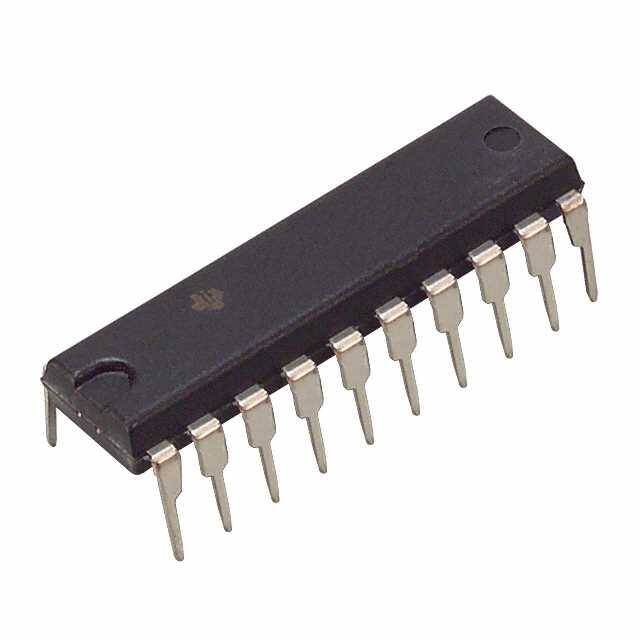
SN75ALS056 . . . DW OR N PACKAGE
(TOP VIEW)
A1
A2
A3
A4
1
20
2
19
3
18
4
17
VCC
A5
A6
A7
A8
CS
5
16
6
15
7
14
8
13
9
12
10
11
B1
B2
B3
B4
GND
B5
B6
B7
B8
T/R
SN75ALS057 . . . DW OR N PACKAGE
(TOP VIEW)
description
The SN75ALS056 is an eight-channel,
monolithic, high-speed, advanced low-power
Schottky (ALS) device designed for two-way data
communication in a densely populated
backplane. The SN75ALS057 is a four-channel
version with independent driver-input (Dn) and
receiver-output (Rn) pins and a separate driver
disable for each driver (En).
D1
R1
D2
R2
1
20
2
19
3
18
4
17
VCC
D3
R3
D4
R4
TE
5
16
6
15
7
14
8
13
9
12
10
11
B1
E1
B2
E2
GND
B3
E3
B4
E4
RE
These transceivers feature open-collector driver outputs with series Schottky diodes to reduce capacitive
loading to the bus. By using a 2-V pullup termination on the bus, the output signal swing is approximately 1 V,
which reduces the power necessary to drive the bus load capacitance. The driver outputs generate trapezoidal
waveforms that reduce crosstalk between channels. The drivers are capable of driving an equivalent dc load
as low as 18.5 Ω. The receivers have internal low-pass filters to further improve noise immunity.
The SN75ALS056 and SN75ALS057 are characterized for operation from 0°C to 70°C.
Please be aware that an important notice concerning availability, standard warranty, and use in critical applications of
Texas Instruments semiconductor products and disclaimers thereto appears at the end of this data sheet.
† The transceivers are suitable for IEEE Standard 896 applications to the extent of the operating conditions and characteristics specified in this
data sheet.
Copyright 1998, Texas Instruments Incorporated
PRODUCTION DATA information is current as of publication date.
Products conform to specifications per the terms of Texas Instruments
standard warranty. Production processing does not necessarily include
testing of all parameters.
POST OFFICE BOX 655303
• DALLAS, TEXAS 75265
1
�SN75ALS056, SN75ALS057
TRAPEZOIDAL-WAVEFORM INTERFACE BUS TRANSCEIVERS
SLLS028G – AUGUST 1987 – REVISED JUNE 1998
logic symbol†
SN75ALS056
T/R
11
3EN1 (A-B)
3EN2 (B-A)
CS
A1
10
G3
1
1
20
B1
2
A2
A3
A4
2
19
3
18
4
17
6
15
A5
A6
A7
A8
B2
B3
B4
B5
7
14
8
13
9
12
B6
B7
B8
SN75ALS057
TE
RE
D1
E1
R1
D2
E2
R2
D3
E3
R3
D4
E4
R4
10
11
EN1 (D-B)
EN2 (B-R)
1
&
19
2
1
20
B1
2
3
18
17
B2
4
6
15
14
B3
7
8
12
13
B4
9
† These symbols are in accordance with ANSI/IEEE Std 91-1984 and IEC Publication 617-12.
2
POST OFFICE BOX 655303
• DALLAS, TEXAS 75265
�SN75ALS056, SN75ALS057
TRAPEZOIDAL-WAVEFORM INTERFACE BUS TRANSCEIVERS
SLLS028G – AUGUST 1987 – REVISED JUNE 1998
logic diagram (positive logic)
SN75ALS056
T/R
CS
11
10
Xmit
20
A1
1
B1
Rcv
12
A8
9
B8
SN75ALS057
TE
RE
10
11
Xmit
D1
E1
R1
1
20
B1
19
2
Rcv
D4
E4
R4
8
13
B4
12
9
† These symbols are in accordance with ANSI/IEEE Std 91-1984 and IEC Publication 617-12.
POST OFFICE BOX 655303
• DALLAS, TEXAS 75265
3
�SN75ALS056, SN75ALS057
TRAPEZOIDAL-WAVEFORM INTERFACE BUS TRANSCEIVERS
SLLS028G – AUGUST 1987 – REVISED JUNE 1998
Function Tables
SN75ALS056
TRANSMIT/RECEIVE
CONTROLS
CHANNELS
A↔B
CS
T/R
L
H
T(A
B)
L
L
R(B
A)
H
X
D
SN75ALS057
TRANSMIT/RECEIVE
CONTROLS
CHANNELS
TE
RE
En
L
L
L
D
D
B
B
R
R
L
L
H
T
R
L
H
L
D
D
L
H
H
T
D
H
L
X
D
R
H
H
X
D
D
H = high level, L = low level, R = receive, T = transmit,
D = disable, X = irrelevant
Direction of data transmission is from An to Bn for the SN75ALS056 and from Dn to Bn for the SN75ALS057.
Direction of data reception is from Bn to An for the SN75ALS056 and from Bn to Rn for the SN75ALS057. Data
transfer is inverting in both directions.
4
POST OFFICE BOX 655303
• DALLAS, TEXAS 75265
�SN75ALS056, SN75ALS057
TRAPEZOIDAL-WAVEFORM INTERFACE BUS TRANSCEIVERS
SLLS028G – AUGUST 1987 – REVISED JUNE 1998
schematics of inputs and outputs
DRIVER OUTPUT
RECEIVER INPUT
CONTROL INPUTS
VCC
VCC
17.5 kΩ
Bn
2.5 kΩ
15 kΩ
TE/RE
Input
ESD
Protect
ESD
Protect
40 µA
GND
GND
RECEIVER OUTPUT
DRIVER INPUT
VCC
48 Ω
20 kΩ
SN75ALS057
Only
An
or
Rn-Dn
ESD
Protect
En
ESD
Protect†
ESD
Protect
GND
All resistor values shown are nominal.
† Additional ESD protection is on the SN75ALS057, which has separate receiver-output and driver-input pins.
absolute maximum ratings over operating free-air temperature (unless otherwise noted)‡
Supply voltage, VCC (see Note 1) . . . . . . . . . . . . . . . . . . . . . . . . . . . . . . . . . . . . . . . . . . . . . . . . . . . . . . . . . . . . . 6 V
Control input voltage, VI . . . . . . . . . . . . . . . . . . . . . . . . . . . . . . . . . . . . . . . . . . . . . . . . . . . . . . . . . . . . . . . . . . . 5.5 V
Driver input voltage, VI . . . . . . . . . . . . . . . . . . . . . . . . . . . . . . . . . . . . . . . . . . . . . . . . . . . . . . . . . . . . . . . . . . . . 5.5 V
Driver output voltage, VO . . . . . . . . . . . . . . . . . . . . . . . . . . . . . . . . . . . . . . . . . . . . . . . . . . . . . . . . . . . . . . . . . . 2.5 V
Receiver input voltage, VI . . . . . . . . . . . . . . . . . . . . . . . . . . . . . . . . . . . . . . . . . . . . . . . . . . . . . . . . . . . . . . . . . . 2.5 V
Receiver output voltage, VO . . . . . . . . . . . . . . . . . . . . . . . . . . . . . . . . . . . . . . . . . . . . . . . . . . . . . . . . . . . . . . . 5.5 V
Continuous total power dissipation . . . . . . . . . . . . . . . . . . . . . . . . . . . . . . . . . . . . . See Dissipation Rating Table
Storage temperature range, Tstg . . . . . . . . . . . . . . . . . . . . . . . . . . . . . . . . . . . . . . . . . . . . . . . . . . . –65°C to 150°C
Lead temperature 1,6 mm (1/16 inch) from case for 10 seconds: DW or N package . . . . . . . . . . . . . . . 260 °C
‡ Stresses beyond those listed under “absolute maximum ratings” may cause permanent damage to the device. These are stress ratings only, and
functional operation of the device at these or any other conditions beyond those indicated under “recommended operating conditions” is not
implied. Exposure to absolute-maximum-rated conditions for extended periods may affect device reliability.
NOTE 1: Voltage values are with respect to network ground terminal.
POST OFFICE BOX 655303
• DALLAS, TEXAS 75265
5
�SN75ALS056, SN75ALS057
TRAPEZOIDAL-WAVEFORM INTERFACE BUS TRANSCEIVERS
SLLS028G – AUGUST 1987 – REVISED JUNE 1998
DISSIPATION RATING TABLE
PACKAGE
TA ≤ 25°C
POWER RATING
DERATING FACTOR
ABOVE TA = 25°C
TA = 70°C
POWER RATING
TA = 125°C
POWER RATING
DW
1025 mW
8.2 mW/°C
656 mW
—
N
1150 mW
9.2 mW/°C
736 mW
—
recommended operating conditions
Supply voltage, VCC
High-level driver and control input voltage, VIH
MIN
NOM
MAX
UNIT
4.75
5
5.25
V
2
V
Low-level driver and control input voltage, VIL
0.8
Bus termination voltage
Operating free-air temperature, TA
V
1.9
2.1
V
0
70
°C
electrical characteristics over recommended ranges of supply voltage and operating free-air
temperature (unless otherwise noted)
TEST CONDITIONS†
PARAMETER
VIK
VIT
VOH
VOL
Input clamp voltage at An, T/R, or CS
An
Bn at 2 V ,CS at 0.8 V,
T/R at 0.8 V, IOL = 16 mA
Bn
An at 2 V, CS at 0.8 V,
T/R at 2 V, VL = 2 V,
RL =18.5 Ω,, See Figure 1
An, T/R or CS
IIH
High-level input current
IIL
Low level input current at An, T/R, or CS
IOS
Short-circuit output current at An
ICC
CO(B)
Supply current
Bn
VI = 0.4 V
An at 0, Bn at 1.2 V,
CS at 0.8 V, T/R at 0.8 V
• DALLAS, TEXAS 75265
UNIT
–1.5
V
1.69
V
V
0.5
V
0.75
1.2
40
100
–40
4.5
POST OFFICE BOX 655303
MAX
2.4
VI = VCC
VI = 2 V, VCC = 0 or 5.25 V,
An at 0.8 V, T/R at 0.8 V
Driver output capacitance
† Typical values are at VCC = 5 V, TA = 25°C.
6
TYP†
1.405
Bn at 1.2 V, CS at 0.8 V,
T/R at 0.8V, IOH = – 400 µA
Low-level output voltage
MIN
II = –18 mA
Receiver input threshold voltage at Bn
High-level output voltage at An
SN75ALS056
µA
–400
µA
–120
mA
75
mA
pF
�SN75ALS056, SN75ALS057
TRAPEZOIDAL-WAVEFORM INTERFACE BUS TRANSCEIVERS
SLLS028G – AUGUST 1987 – REVISED JUNE 1998
electrical characteristics over recommended ranges of supply voltage and operating free-air
temperature (unless otherwise noted)
PARAMETER
VIK
VIT
VOH
VOL
IIH
TEST CONDITIONS
Input clamp voltage at Dn, En, TE, or RE
SN75ALS057
TYP†
MAX
MIN
II = –18 mA
Receiver input threshold voltage at Bn
1.41
Bn at 1.2 V, RE at 0.8 V,
IOH = –400 µA
High-level output voltage at Rn
Rn
Bn at 2 V, RE at 0.8 V,
IOL = 16 mA
Bn
Dn at 2 V, En at 2 V,
TE at 0.8 V, VL = 2 V,
RL = 18.5 Ω, See Figure 1
Dn, En,
TE, or RE
VI = VCC
Bn
VI = 2 V, VCC = 0 or 5.25 V,
Dn at 0.8 V, En at 0.8 V,
TE at 0.8 V
Low-level output voltage
High-level input current
IIL
Low-level input current at Dn, En, TE, or RE
IOS
Short-circuit output current at Rn
ICC
CO(B)
Supply current
UNIT
–1.5
V
1.69
V
2.4
V
0.5
V
0.75
1.2
40
VI = 0.4 V
Rn at 0, Bn at 1.2 V,
RE at 0.8 V
µA
100
–40
Driver output capacitance
–400
µA
–120
mA
40
mA
4.5
pF
† Typical values are at VCC = 5 V, TA = 25°C.
switching characteristics over recommended ranges of supply voltage and operating free-air
temperature (unless otherwise noted)
PARAMETER
tPLH1
Propagation delay time,
low-to-high-level output
tPHL1
Propagation delay time,
high-to-low-level output
tPLH2
Propagation delay time,
low-to-high-level output
FROM
(INPUT)
TO
(OUTPUT)
CS
Bn
An
tPHL2
Propagation delay time
high-to-low-level output
tPLH3
Propagation delay time,
low-to-high-level output
tPHL3
Propagation delay time,
high-to-low-level output
tTLH
Transition time,
low-to-high-level output
T/R
tTHL
Transition time,
high-to-low-level output
An
Bn
Bn
Bn
TEST CONDITIONS
SN75ALS056
DRIVER
MIN
TYP†
24
An and T/R at 2 V, VL = 2 V,
RL1 = 18 Ω,,
Ω CL = 30 pF
pF,
RL2 not connected, See Figure 2
ns
20
CS at 0.8 V, T/R at 2 V,
VL = 2 V, RL1 = 18 Ω,,
RL2 not connected,
connected CL = 30 pF
pF,
See Figure 2,
19
ns
18
VI(An) = 5 V, CS at 0.8 V,
RL1 = 18 Ω, CL = 30 pF,
connected VL = 2 V,
V
RL2 not connected,
See Figure 3,
CS at 0.8 V, T/R at 2 V,
VL = 2 V,, CL = 30 pF,,
RL1 = 18 Ω, RL2 not connected,
See Figure 2
UNIT
MAX
25
ns
35
1
3
11
1
3
6
ns
† Typical values are at VCC = 5 V, TA = 25°C
POST OFFICE BOX 655303
• DALLAS, TEXAS 75265
7
�SN75ALS056, SN75ALS057
TRAPEZOIDAL-WAVEFORM INTERFACE BUS TRANSCEIVERS
SLLS028G – AUGUST 1987 – REVISED JUNE 1998
switching characteristics over recommended ranges of supply voltage and operating free-air
temperature (unless otherwise noted)
PARAMETER
tPLH4
8
Propagation delay time,
low-to-high-level output
FROM
(INPUT)
TO
(OUTPUT)
Bn
An
tPHL4
Propagation delay time,
high-to-low-level output
tPLZ1
Output disable time from
low level
T/R
An
tPZL1
Output enable time to
low level
T/R
An
tPHZ1
Output disable time from
high level
T/R
An
tPZH1
Output enable time to
high level
T/R
An
tPLZ2
Output disable time from
low level
CS
An
tPZL2
Output enable time to
low level
CS
An
tPHZ2
Output disable time from
high level
CS
An
tPZH2
Output enable time to
high level
CS
An
tw(NR)
Receiver noise rejection
pulse duration
Bn
An
TEST CONDITIONS
SN75ALS056
RECEIVER
MIN
18
CS at 0.8 V,, T/R at 0.8 V,, RL1 = 390 Ω,,
RL2 = 1.6 kΩ, CL = 30 pF, See Figure 4
ns
18
CS at 0.8 V, VI(Bn) = 2 V, VL = 5 V,
RL1 = 390 Ω, RL2 not connected,
CL = 15 pF, See Figure 3
CS at 0.8 V, VI(Bn) = 2 V, VL = 5 V,
RL1 = 390 Ω, RL2 = 1.6 kΩ,
CL = 30 pF, See Figure 3
CS at 0.8 V, VI(Bn) = 0, VL = 0,
RL1 = 390 Ω, RL2 not connected,
CL = 15 pF, See Figure 3
CS at 0.8 V, VI(Bn) = 0, VL = 0,
RL1 not connected, RL2 = 1.6 kΩ,
CL = 30 pF, See Figure 3
Bn at 2 V, T/R at 0.8 V, CL = 5 pF,
VL = 5 V, RL1 = 390 Ω,
RL2 not connected, See Figure 5
Bn at 2 V, T/R at 0.8 V, CL = 30 pF,
VL = 5 V, RL1 = 390 Ω, RL2 = 1.6 kΩ,
See Figure 5
Bn at 0.8 V, T/R at 0.8 V, CL = 5 pF,
VL = 0, RL1 = 390 Ω,
RL2 not connected, See Figure 5
Bn at 0.8 V, T/R at 0.8 V, CL = 30 pF,
VL = 0, RL1 not connected,
RL2 = 1.6 kΩ, See Figure 5
CS at 0.8 V, T/R at 0.8 V, RL1 = 390 Ω,
RL2 = 1.6 kΩ, CL = 30 pF, VL = 5 V,
See Figure 6
POST OFFICE BOX 655303
• DALLAS, TEXAS 75265
UNIT
MAX
3
20
ns
40
ns
17
ns
15
ns
18
ns
15
ns
8
ns
17
ns
ns
�SN75ALS056, SN75ALS057
TRAPEZOIDAL-WAVEFORM INTERFACE BUS TRANSCEIVERS
SLLS028G – AUGUST 1987 – REVISED JUNE 1998
switching characteristics over recommended ranges of supply voltage and operating free-air
temperature (unless otherwise noted)
PARAMETER
tPLH1
TO
(OUTPUT)
TE
Bn
Propagation delay time,
low-to-high-level output
tPHL1
Propagation delay time,
high-to-low-level output
tPLH2
Propagation delay time,
low-to-high-level output
tPHL2
Propagation delay time,
high-to-low-level output
tTLH
Transition time,
low-to-high-level output
tTHL
FROM
(INPUT)
Transition time,
high-to-low-level output
Dn or En
Dn or En
Bn
Bn
TEST CONDITIONS
SN75ALS057
DRIVER
MIN
TYP†
UNIT
MAX
Dn, En, RE at 2 V, VL = 2 V,
RL2 not connected
connected, RL1 = 18 Ω,
Ω
See Figure 2, CL = 30 pF
24
TE at 0.8 V, RE at 2 V,
VL = 2 V, RL1 = 18 Ω,
RL2 not connected,CL = 30 pF,
See Figure 2
19
RE at 2 V, VL = 2 V,
TE at 0.8 V,, RL1 = 18 Ω,,
,,
RL2 not connected, CL = 30 pF,
See Figure 2
ns
20
ns
18
1
3
11
1
3
6
ns
† Typical values are at VCC = 5 V, TA = 25°C.
switching characteristics over recommended ranges of supply voltage and operating free-air
temperature (unless otherwise noted) (continued)
PARAMETER
tPLH4
Propagation delay time,
low-to-high-level output
FROM
(INPUT)
TO
(OUTPUT)
Bn
Rn
tPHL4
Propagation delay time,
high-to-low-level output
tPLZ2
Output disable time
from low level
RE
Rn
tPZL2
Output enable time to
low level
RE
Rn
tPHZ2
Output disable time
from high level
RE
Rn
tPZH2
Output enable time to
high level
RE
Rn
tw(NR)
Receiver noise
rejection pulse duration
Bn
Rn
TEST CONDITIONS
SN75ALS057
RECEIVER
MIN
18
RE at 0.8 V, TE at 2 V, VL = 5 V,
RL1 = 390 Ω,,
Ω RL2 = 1.6
1 6 kΩ,,
kΩ CL = 30 pF,
pF
See Figure 4
ns
18
Bn at 2 V, TE at 2 V, VL = 5 V,
CL = 5 pF, RL1 = 390 Ω,
RL2 not connected, See Figure 5
Bn at 2 V, TE at 2 V, VL = 5 V,
CL = 30 pF, RL1 = 390 Ω, RL2 = 1.6 kΩ,
See Figure 5
Bn at 0.8 V, TE at 2 V, VL = 0,
CL = 5 pF, RL1 = 390 Ω,
RL2 not connected, See Figure 5
Bn at 0.8 V, TE at 2 V, VL = 0,
CL = 30 pF, RL1 not connected,
RL2 = 1.6 kΩ, See Figure 5
TE at 2 V, RE at 0.8 V, VL = 0,
RL1 = 390 Ω, RL2 = 1.6 kΩ, CL = 30 pF,
See Figure 6
POST OFFICE BOX 655303
• DALLAS, TEXAS 75265
UNIT
MAX
3
18
ns
15
ns
17
ns
17
ns
ns
9
�SN75ALS056, SN75ALS057
TRAPEZOIDAL-WAVEFORM INTERFACE BUS TRANSCEIVERS
SLLS028G – AUGUST 1987 – REVISED JUNE 1998
switching characteristics over recommended ranges of supply voltage and operating free-air
temperature (unless otherwise noted) (continued)
FROM
((INPUT))
PARAMETER
TO
(OUTPUT)
(
)
TEST CONDITIONS
SN75ALS057
DRIVER PLUS
RECEIVER
MIN
tPLH6
tPHL6
Propagation delay time,
low-to-high-level output
Propagation delay time,
high-to-low-level output
Dn
Rn
RE at 0.8 V, TE at 0.8 V, RL1 = 390 Ω,
RL2 = 1.6 kΩ,, CL = 30 pF, See Figure 7
PARAMETER MEASUREMENT INFORMATION
VL
SN75ALS056
or
SN75ALS057
RL1
(Bn)
VO
Figure 1. Driver Low-Level-Output-Voltage Test Circuit
10
POST OFFICE BOX 655303
• DALLAS, TEXAS 75265
UNIT
MAX
40
ns
40
�SN75ALS056, SN75ALS057
TRAPEZOIDAL-WAVEFORM INTERFACE BUS TRANSCEIVERS
SLLS028G – AUGUST 1987 – REVISED JUNE 1998
PARAMETER MEASUREMENT INFORMATION
VL
RL1
VI(CS, TE, An, Dn, En)
SN75ALS056
or
SN75ALS057
VO
(Bn)
CL (includes jig capacitance)
RL2
TEST CIRCUIT
3V
1.5 V
1.5 V
CS, TE
0
tPLH1
VI
tPHL1
3V
1.5 V
(An, Dn, En)
1.5 V
0
tPHL2
tPLH2
VOH
VO(Bn)
VOL
1.55 V
10%
90%
tTLH
90%
1.55 V
10%
tTHL
VOLTAGE WAVEFORMS
NOTE A: tr = tf ≤ 5 ns from 10% to 90%
Figure 2. Driver Test Circuit and Voltage Waveforms
POST OFFICE BOX 655303
• DALLAS, TEXAS 75265
11
�SN75ALS056, SN75ALS057
TRAPEZOIDAL-WAVEFORM INTERFACE BUS TRANSCEIVERS
SLLS028G – AUGUST 1987 – REVISED JUNE 1998
PARAMETER MEASUREMENT INFORMATION
5V
390 Ω
VL
S1
RL1
VI(T/R)
SN75ALS056
VI(An, Bn)
VO
(Bn,An)
RL2
15 pF
S2
CL (includes jig capacitance)
1.6 kΩ
TEST CIRCUIT
VI(T/R) 3 V
0
1.5 V
1.5 V
tPLH3
tPHL3
VO(Bn)
1.55 V
1.55 V
tPLZ1
tPZL1
1.5 V
VO(An)
0.5 V
tPZH1
0.5 V
tPHZ1
VO(An)
1.5 V
S1 Closed
S2 Open
S1 Open
S2 Closed
VOLTAGE WAVEFORMS
NOTE A: tr = tf ≤ 5 ns from 10% to 90%
Figure 3. Propagation Delay From T/R to An or Bn Test Circuit and Voltage Waveforms
12
POST OFFICE BOX 655303
• DALLAS, TEXAS 75265
�SN75ALS056, SN75ALS057
TRAPEZOIDAL-WAVEFORM INTERFACE BUS TRANSCEIVERS
SLLS028G – AUGUST 1987 – REVISED JUNE 1998
5V
RL1
SN75ALS056
or
SN75ALS057
VI(Bn)
VO
(An,Rn)
RL2
CL (includes jig capacitance)
TEST CIRCUIT
2V
VI(Bn)
1.55 V
1.55 V
1V
tPLH4
tPHL4
VOH
VO(An, Rn)
1.5 V
1.5 V
VOL
VOLTAGE WAVEFORMS
NOTE A: tr = tf ≤ 5 ns from 10% to 90%
Figure 4. Receiver Test Circuit and Voltage Waveforms
VL
RL1
SN75ALS056
or
SN75ALS057
VI(CS, RE)
VO
(An,Rn)
RL2
CL (includes jig capacitance)
TEST CIRCUIT
3V
VI(CS, RE)
0
1.5 V
1.5 V
tPHZ2
0.5 V
VO(An, Rn)
tPZH2
1.5 V
tPLZ2
0.5 V
VO(An, Rn)
tPZL2
1.5 V
VOLTAGE WAVEFORMS
NOTE A: tr = tf ≤ 5 ns from 10% to 90%
Figure 5. Propagation Delay From CS to An or RE to Rn Test Circuit and Voltage Waveforms
POST OFFICE BOX 655303
• DALLAS, TEXAS 75265
13
�SN75ALS056, SN75ALS057
TRAPEZOIDAL-WAVEFORM INTERFACE BUS TRANSCEIVERS
SLLS028G – AUGUST 1987 – REVISED JUNE 1998
PARAMETER MEASUREMENT INFORMATION
5V
RL1
SN75ALS056
or
SN75ALS057
VI(Bn)
VO
(An, Rn)
RL2
CL (includes jig capacitance)
TEST CIRCUIT
Bus Logic
High Level
1.85 V
2V
1.55 V
V1
1.55 V
1.1 V
1.25 V
Bus Logic
Low Level
tw(NR)
tw(NR)
tw is increased until the output voltage
fall just reaches 2 V.
tw is increased until the output voltage rise
just reaches 0.8 V.
VOLTAGE WAVEFORMS
NOTE A: tr = tf ≤ 5 ns from 10% to 90%
Figure 6. Receiver Noise-Immunity Test Circuit and Voltage Waveforms
2V
5V
VI(Dn)
RL1
18 Ω
(Bn)
SN75ALS057
VO
(Rn)
RL2
30 pF
CL (includes jig capacitance)
TEST CIRCUIT
3V
1.5 V
1.5 V
VI(Dn)
0
tPHL6
tPLH6
VO(Rn)
1.5 V
1.5 V
VOLTAGE WAVEFORMS
NOTE A: tr = tf ≤ 5 ns from 10% to 90%
Figure 7. Driver Plus Receiver Delay-Times Test Circuits and Voltage Waveforms
14
POST OFFICE BOX 655303
• DALLAS, TEXAS 75265
�PACKAGE OPTION ADDENDUM
www.ti.com
23-Apr-2022
PACKAGING INFORMATION
Orderable Device
Status
(1)
Package Type Package Pins Package
Drawing
Qty
Eco Plan
(2)
Lead finish/
Ball material
MSL Peak Temp
Op Temp (°C)
Device Marking
(3)
(4/5)
(6)
SN75ALS056DW
ACTIVE
SOIC
DW
20
25
RoHS & Green
NIPDAU
Level-1-260C-UNLIM
0 to 70
75ALS056
SN75ALS057DW
ACTIVE
SOIC
DW
20
25
RoHS & Green
NIPDAU
Level-1-260C-UNLIM
0 to 70
75ALS057
SN75ALS057DWR
ACTIVE
SOIC
DW
20
2000
RoHS & Green
NIPDAU
Level-1-260C-UNLIM
0 to 70
75ALS057
(1)
The marketing status values are defined as follows:
ACTIVE: Product device recommended for new designs.
LIFEBUY: TI has announced that the device will be discontinued, and a lifetime-buy period is in effect.
NRND: Not recommended for new designs. Device is in production to support existing customers, but TI does not recommend using this part in a new design.
PREVIEW: Device has been announced but is not in production. Samples may or may not be available.
OBSOLETE: TI has discontinued the production of the device.
(2)
RoHS: TI defines "RoHS" to mean semiconductor products that are compliant with the current EU RoHS requirements for all 10 RoHS substances, including the requirement that RoHS substance
do not exceed 0.1% by weight in homogeneous materials. Where designed to be soldered at high temperatures, "RoHS" products are suitable for use in specified lead-free processes. TI may
reference these types of products as "Pb-Free".
RoHS Exempt: TI defines "RoHS Exempt" to mean products that contain lead but are compliant with EU RoHS pursuant to a specific EU RoHS exemption.
Green: TI defines "Green" to mean the content of Chlorine (Cl) and Bromine (Br) based flame retardants meet JS709B low halogen requirements of


 工商网监
湘ICP备2023018690号
工商网监
湘ICP备2023018690号
