SN75ALS085
LAN ACCESS UNIT INTERFACE DUAL DRIVER/RECEIVER
SLLS054D – APRIL 1989 – REVISED OCTOBER 2001
D
D
D
D
D
D
D
D
D
D
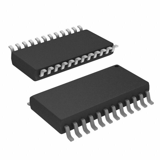
DW OR NT PACKAGE
(TOP VIEW)
Meets or Exceeds the Requirements of IOS
8802.3:1989 and ANSI/IEEE Std 802.3-1988
Interdevice Loopback Paths for System
Testing
Squelch Function Implemented on the
Receiver Inputs
Drives a Balanced 78-Ω Load
Transformer Coupling Not Required in
System
Power-Up/Power-Down Protection (Glitch
Free)
Isolated Ground Pins for Reduced Noise
Coupling
Fault-Condition Protection Built Into the
Device
Driver Inputs Are Level-Shifted ECL
Compatible
Package Options Include Plastic
Small-Outline (DW) Package and Standard
Plastic (NT) DIP
TXI1
TXEN1
LOOP1
GND
RXEN1
RXO1
RXO2
RXEN2
GND
LOOP2
TXEN2
TXI2
1
24
2
23
3
22
4
21
5
20
6
19
7
18
8
17
9
16
10
15
11
14
12
13
TXO1
TXO1
VCC
RXI1
RXI1
GND
GND
RXI2
RXI2
VCC
TXO2
TXO2
description
The SN75ALS085 is a high-speed, advanced low-power Schottky, dual-channel driver/receiver device
designed for use in the AUI of ANSI/IEEE Std 802.3-1988. The two drivers on the device drive a 78-Ω balanced,
terminated twisted-pair transmission line up to a maximum length of 50 meters. In the off (idle) state, the drivers
maintain minimal differential output voltage on the twisted-pair line and, at the same time, remain within the
required output common-mode range.
With the driver enable (TXEN) high, upon receiving the first falling edge into the driver input, the differential
outputs rise to full-amplitude output levels within 25 ns. The output amplitude is maintained for the remainder
of the packet. After the last positive packet edge is transmitted into the driver, the driver maintains a minimum
of 70% full differential output for a minimum of 200 ns, then decays to a minimum level for the reset (idle)
condition within 8 µs. Disabling the driver by taking the driver enable low also forces the output into the idle
condition after the normal 8-µs timeout. While operating, the drivers are able to withstand a set of fault conditions
and not suffer damage due to the faults being applied. The drivers power up in the idle state to ensure that no
activity is placed on the twisted-pair cable, which could be interpreted as network traffic.
The line receiver squelch function interfaces to a differential twisted-pair line terminated external to the device.
The receiver squelch circuit allows differential receive signals to pass through, as long as the input amplitude
and pulse duration are greater than the minimum squelch threshold. This ensures a good signal-to-noise ratio
while the data path is active and prevents system noise from causing false data transitions during line shutdown
and line-idle conditions. The receiver outputs (RXO) default to a high level and the receiver-enable (RXEN)
outputs default to a low level while the squelch function is blocking the data path through the receiver (idle). The
line receiver squelch becomes active within 50 ns when the input squelch threshold is exceeded. RXEN is driven
high when the squelch circuit allows data to pass through the receiver. The receiver squelch circuit also can
withstand a set of fault conditions while operating, without causing permanent damage to the device.
Please be aware that an important notice concerning availability, standard warranty, and use in critical applications of
Texas Instruments semiconductor products and disclaimers thereto appears at the end of this data sheet.
Copyright 2001, Texas Instruments Incorporated
PRODUCTION DATA information is current as of publication date.
Products conform to specifications per the terms of Texas Instruments
standard warranty. Production processing does not necessarily include
testing of all parameters.
POST OFFICE BOX 655303
• DALLAS, TEXAS 75265
1
�SN75ALS085
LAN ACCESS UNIT INTERFACE DUAL DRIVER/RECEIVER
SLLS054D – APRIL 1989 – REVISED OCTOBER 2001
description (continued)
The purpose of the loop functions is to provide a means by which system data-path verification can be done
to isolate faulty interfaces and assist in network diagnosis. The LOOP pins are TTL compatible and must be
held high for normal operation. When LOOP1 is taken low, the output of driver 1 (TXO1) immediately goes into
the idle state. Also, the input to receiver 1 is ignored, and a path from a transmit input (TXI1) to RXO1 is
established. When LOOP1 is taken back high, driver 1 and receiver 1 revert back to their normal operation.
When LOOP2 is taken low, a similar data path is established between TXI1 and RXO2. TXEN1 must be high
for the loop functions to operate, and TXEN1 can be used to gate the loop function if desired. During loop
operation, the respective RXEN reflects the status of TXEN1.
The SN75ALS085 is characterized for operation from 0°C to 70°C.
AVAILABLE OPTIONS
PACKAGED DEVICES
TA
PLASTIC
SMALL OUTLINE
(DW)
PLASTIC DIP
(NT)
0°C to 70°C
SN75ALS085DW
SN75ALS085NT
The DW package is available taped and reeled. Add the suffix R
to device type (e.g., SN75ALS085DWR).
Function Tables
RECEIVER (LOOP = H)
OUTPUTS
PREVIOUS
RXEN
RXI
VID = 1315 mV to –175 mV,
VID = –275 mV to –1315 mV
tw < 25 ns
tw > 50 ns
VID = 318 mV to 1315 mV,
VID = 318 mV to 1315 mV,
tw < 142 ns
tw > 187 ns
RXEN
RXO
L
L
H
X
H
L
H
H
H
X
L
H
H = high level, L = low level, X = don’t care
DRIVER (LOOP = H)
TXI
TXEN
PREVIOUS
TXO
OUTPUT
TXO
L
L
Idle
Idle
H
L
Idle
Idle
↓
H
Idle
L
L
H
Active
L
H < 260 µs
H
Active
H
H > 8 µs
H
Active
Idle
L
L > 8 µs
Active
Idle
H < 260 ns
L > 8 µs
Active
Idle
H < 260 ns
L < 260 ns
Active
H
H > 8 µs
L < 260 ns
Active
Idle
L
L < 260 ns
Active
L
H = VI ≥ VT max, L = VI ≤ VT min
2
POST OFFICE BOX 655303
• DALLAS, TEXAS 75265
�SN75ALS085
LAN ACCESS UNIT INTERFACE DUAL DRIVER/RECEIVER
SLLS054D – APRIL 1989 – REVISED OCTOBER 2001
Function Tables (continued)
LOOP
INPUTS
LOOP1
LOOP2
L
L
OUTPUTS
TXI1
TXEN1
RXI1
RXI2
L
L
H
X
X
L
H
H
X
X
L
L
X
L
X
X
L
H
L
H
X
L
H
H
H
X
RXO1
RXO2
RXEN1
RXEN2
TXO1
L
L
H
H
Idle
H
H
H
H
Idle
H
H
L
L
Idle
Normal
L
Normal
H
Normal
Idle
Normal
H
Normal
H
Normal
Idle
Idle
L
H
X
L
X
Normal
H
Normal
L
Normal
H
L
L
H
Normal
X
Normal
L
Normal
H
Idle
H
L
H
H
Normal
X
Normal
H
Normal
H
Idle
H
L
X
L
Normal
X
Normal
H
Normal
L
Idle
H
H
Normal
Normal
Normal
Normal
Normal
Normal
Normal
Normal
Normal
H = high level, L = low level, X = don’t care
POST OFFICE BOX 655303
• DALLAS, TEXAS 75265
3
�SN75ALS085
LAN ACCESS UNIT INTERFACE DUAL DRIVER/RECEIVER
SLLS054D – APRIL 1989 – REVISED OCTOBER 2001
logic diagram (positive logic)
RXI1
RXI1
20
21
+
–
225 mV
Noise
Filter
5
6
LOOP1
TXI1
TXEN1
LOOP2
3
1
24
23
ECL/TTL
2
250 ns
4 µS
X1
TXI2
TXEN2
4
RXO1
TXO1
TXO1
1
1
10
7
RXI2
RXI2
RXEN1
150 ns
17
16
+
–
225 mV
12
11
150 ns
Noise
Filter
8
14
13
ECL/TTL
250 ns
4 µS
POST OFFICE BOX 655303
• DALLAS, TEXAS 75265
X1
1
1
RXO2
RXEN2
TXO2
TXO2
�SN75ALS085
LAN ACCESS UNIT INTERFACE DUAL DRIVER/RECEIVER
SLLS054D – APRIL 1989 – REVISED OCTOBER 2001
schematics of inputs and outputs
RXI and RXI Inputs
LOOP and TXEN Inputs
VCC
VCC
20 kΩ
4 kΩ
4 kΩ
4 kΩ
RXI
RXI
4 kΩ
ESD
LOOP,
TXEN
ESD
3 kΩ
4 kΩ
ESD
+
1 kΩ
–
TXI Inputs
RXO and RXEN Outputs
VCC
VCC
50 Ω
200 Ω
TXI
ESD
50 kΩ
RXO,
RXEN
5 kΩ
ESD
POST OFFICE BOX 655303
• DALLAS, TEXAS 75265
5
�SN75ALS085
LAN ACCESS UNIT INTERFACE DUAL DRIVER/RECEIVER
SLLS054D – APRIL 1989 – REVISED OCTOBER 2001
absolute maximum ratings over operating free-air temperature range (unless otherwise noted)†
Supply voltage, VCC (see Note 1) . . . . . . . . . . . . . . . . . . . . . . . . . . . . . . . . . . . . . . . . . . . . . . . . . . . . . . . . . . . . . 6 V
TXI and LOOP input voltage, VI . . . . . . . . . . . . . . . . . . . . . . . . . . . . . . . . . . . . . . . . . . . . . . . . . . . . . . . . . . . . . 5.5 V
TXO and TXO output voltage, VO . . . . . . . . . . . . . . . . . . . . . . . . . . . . . . . . . . . . . . . . . . . . . . . . . . . . . . . . . . . . 16 V
RXI and RXI input voltage, VI . . . . . . . . . . . . . . . . . . . . . . . . . . . . . . . . . . . . . . . . . . . . . . . . . . . . . . . . . . . . . . . . 16 V
RXO and RXEN output voltage, VO . . . . . . . . . . . . . . . . . . . . . . . . . . . . . . . . . . . . . . . . . . . . . . . . . . . . . . . . . 5.5 V
Package thermal impedance, θJA (see Notes 2 and 3): DW package . . . . . . . . . . . . . . . . . . . . . . . . . . 46°C/W
(see Notes 2 and 4): NT package . . . . . . . . . . . . . . . . . . . . . . . . . . . 67°C/W
Lead temperature 1,6 mm (1/16 inch) from case for 10 seconds . . . . . . . . . . . . . . . . . . . . . . . . . . . . . . . 260°C
Storage temperature range, Tstg . . . . . . . . . . . . . . . . . . . . . . . . . . . . . . . . . . . . . . . . . . . . . . . . . . . . . –65 to 150°C
† Stresses beyond those listed under “absolute maximum ratings” may cause permanent damage to the device. These are stress ratings only, and
functional operation of the device at these or any other conditions beyond those indicated under “recommended operating conditions” is not
implied. Exposure to absolute-maximum-rated conditions for extended periods may affect device reliability.
NOTES: 1. Voltage values are with respect to network ground terminal.
2. Maximum power dissipation is a function of TJ(max), θJA, and TA. The maximum allowable power dissipation at any allowable
ambient temperature is PD = (TJ(max) – TA)/θJA. Operating at the absolute maximum TJ of 150°C can affect reliability.
3. The package thermal impedance is calculated in accordance with JESD 51-7.
4. The package thermal impedance is calculated in accordance with JESD 51-3.
recommended operating conditions
6
MIN
NOM
MAX
UNIT
4.75
5
5.25
V
1
4.2
V
±318
±1315
VCC
VIC
Supply voltage
VID
VIH
Differential voltage between RXI inputs
VIL
IOH
Low-level input voltage, LOOP and TXEN
0.8
High-level output current, RXO and RXEN
– 0.4
mA
IOL
tsu1
Low-level output voltage, RXO and RXEN
16
mA
Setup time, driver mode, TXEN high before TXI↓ (see Figure 7)
10
ns
tsu2
tsu3
Setup time, loop mode, LOOP low before TXEN↑ (see Figure 9)
15
ns
Setup time, loop mode, TXEN high before TXI↓ (see Figure 9)
10
ns
th1
th2
Hold time, loop mode, TXEN high after TXI↑ (see Figure 8)
10
ns
Hold time, loop mode, LOOP low after TXEN↓ (see Figure 8)
15
ns
TA
Operating free-air temperature
Common-mode voltage at RXI inputs
High-level input voltage, LOOP and TXEN
2
0
POST OFFICE BOX 655303
• DALLAS, TEXAS 75265
mV
V
70
V
°C
�SN75ALS085
LAN ACCESS UNIT INTERFACE DUAL DRIVER/RECEIVER
SLLS054D – APRIL 1989 – REVISED OCTOBER 2001
electrical characteristics over recommended ranges of supply voltage and operating free-air
temperature (unless otherwise noted)
PARAMETER
VIK
TEST CONDITIONS
Clamp voltage at all inputs
TA = 0°C
V((TO))
MIN
II = – 18 mA
Driver input (TXI) threshold voltage
TA = 25°C
TA = 70°C
VOD
Driver output (TXO) common-mode voltage
Driver output (TXO) differential voltage
3.752
3.389
3.998
VCC = 5.25 V
VCC = 4.75 V
3.577
4.244
3.213
3.797
VCC = 5 V
VCC = 5.25 V
3.400
4.043
3.588
4.289
VCC = 4.75 V
VCC = 5 V
3.239
3.849
3.426
4.095
VCC = 5.25 V
3.614
4.341
– 275
Idle
LOOP1 at 2 V,
See Figure 1
Active
TXEN at 2 V,
LOOP2 at 2 V,
See Figure 1
Active
1
4.2
LOOP1 at 2 V,
TXI at 3.2 V,
1
4.2
TXEN at 2 V,
LOOP2 at 2 V,
See Figure 1
LOOP1 at 2 V,
TXI at 4.4 V,
1
4.2
Idle
TXEN at 0.8 V,
LOOP2 at 2 V,
LOOP1 at 2 V,
See Figure 1
Active
TXEN at 2 V,
LOOP2 at 2 V,
See Figure 1
LOOP1 at 2 V,
TXI at 3.2 V,
– 600
1315
Active
TXEN at 2 V,
LOOP2 at 2 V,
See Figure 1
LOOP1 at 2 V,
TXI at 4.4 V,
600
1315
High-level output voltage
RXO, RXEN
Low-level output voltage
RXO, RXEN
IIH
High-level input current
TXI
TXEN, LOOP
RXI, RXI
TXEN, LOOP
Low level input current
Low-level
V
3.202
TXEN at 0.8 V,
LOOP2 at 2 V,
VOH
VOL
IIL
UNIT
– 1.5
VCC = 4.75 V
VCC = 5 V
Receiver differential input threshold voltage
VOC
MAX
TXI
RXI, RXI
IOD
Driver differential output current
Idle
IOS
Short-circuit output current†
RXO, RXEN
ICC
Supply current
IOH = – 0.4 mA
IOL = 16 mA
mV
V
± 40
2.4
mV
V
0.5
VI = 2 V
VI = 4.5 V
VID = – 0.5 V,
VI = 0.8 V
V
V
20
400
VIC = 1 V to 4.2 V
µA
1000
– 200
VI = 3.1 V
VI = 0.3 V
100
4
VID = 0.5 V,
TXEN at 0.8 V,
LOOP2 at 2 V,
VIC = 1 V to 4.2 V
LOOP1 at 2 V,
See Figure 2
VO at 0 V,
RXI at 2 V
RXI at 3 V,
LOOP2 at 2 V,
TXI at 4.5 V,
TXEN at 2 V,
Outputs open
10
µA
1000
– 40
±4
mA
– 150
mA
225
mA
† Not more than one output should be shorted at a time, and the duration of the test should not exceed 1 second.
POST OFFICE BOX 655303
• DALLAS, TEXAS 75265
7
�SN75ALS085
LAN ACCESS UNIT INTERFACE DUAL DRIVER/RECEIVER
SLLS054D – APRIL 1989 – REVISED OCTOBER 2001
electrical characteristics over recommended ranges of supply voltage and operating free-air
temperature (unless otherwise noted) (continued)
PARAMETER
Driver fault condition current‡
Receiver fault condition current‡
TEST CONDITIONS
MIN
MAX
TXO shorted to TXO,
Current measured in short
150
TXO at 0 V,
TXO is open,
Current measured at TXO
150
TXO is open,
TXO at 0,
Current measured at TXO
150
TXO at 0 V,
TXO at 0 V,
Current measured at TXO and TXO
150
TXO at 16 V,
TXO is open,
Current measured at TXO
150
TXO is open,
TXO at 16 V,
Current measured at TXO
150
TXO at 16 V,
TXO at 16 V,
Current measured at TXO and TXO
150
RXI shorted to RXI,
Current measured in short
RXI at 0 V,
RXI is open,
Current measured at RXI
3
RXI is open,
RXI at 0 V,
Current measured at RXI
3
UNIT
mA
10
RXI at 0 V,
RXI at 0 V,
Current measured at RXI and RXI
RXI at 16 V,
RXI at open,
Current measured at RXI
10
3
RXI at open,
RXI at 16 V,
Current measured at RXI
10
RXI at 16 V,
RXI at 16 V,
Current measured at RXI and RXI
10
mA
‡ Fault conditions should be measured on only one channel at a time.
switching characteristics over recommended ranges of supply voltage and operating free-air
temperature (unless otherwise noted)
driver
PARAMETER
FROM
(INPUT)
TO
(OUTPUT)
TEST CONDITIONS
MIN
MAX
UNIT
tPLH
Propagation delay time,
low-to-high level output
TXI
TXO, TXO
TXEN at 2 V,
See Figure 3
15
ns
tPHL
Propagation delay time,
high-to-low level output
TXI
TXO, TXO
TXEN at 2 V,
See Figure 3
15
ns
tPIL
Propagation delay time,
idle-to-low level output
TXI
TXO, TXO
TXEN at 2 V,
See Figure 4
25
ns
tPIL
Propagation delay time,
idle-to-low level output
TXEN
TXO, TXO
TXI at 3.2 V,
See Figure 5
25
ns
tw
Output pulse duration, from
low-to-high level to 70% output level
TXO, TXO
TXEN at 2 V,
See Figure 6
8000
ns
VOD(U)
Driver output differential
undershoot voltage
TXI
TXO, TXO
TXEN at 2 V,
See Figure 6
– 100
mV
tsk
Driver caused signal skew
tPLH – tPHL
TXI
TXO, TXO
TXEN at 2 V,
See Figure 3
±3
ns
Rise time, TXO, TXO
TXEN at 2 V,
See Figure 3
1
5
ns
Fall time, TXO, TXO
TXEN at 2 V,
See Figure 3
1
5
ns
tr
tf
8
POST OFFICE BOX 655303
• DALLAS, TEXAS 75265
260
�SN75ALS085
LAN ACCESS UNIT INTERFACE DUAL DRIVER/RECEIVER
SLLS054D – APRIL 1989 – REVISED OCTOBER 2001
receiver
PARAMETER
FROM
(INPUT)
TO
(OUTPUT)
TEST CONDITIONS
MIN
MAX
UNIT
tPLH
Propagation delay time,
low-to-high level output
RXI, RXI
RXO
VIC = 1 V to 4.2 V, See Figure 10
15
ns
tPHL
Propagation delay time,
high-to-low level output
RXI, RXI
RXO
VIC = 1 V to 4.2 V, See Figure 10
15
ns
tPLH
Start-up delay time,
low-to-high level output
RXI, RXI
RXEN
VIC = 1 V to 4.2 V, VID = – 500 mV,
See Figure 12
55
ns
tPHL
Shutdown delay time,
high-to-low level output
RXI, RXI
RXEN
VIC = 1 V to 4.2 V, VID = 500 mV,
See Figure 12
181
ns
tsk
Receiver caused signal
skew (tPLH – tPHL)
RXI, RXI
RXO
VIC = 1 V to 4.2 V, VID = 500 mV,
See Figure 10
±3
ns
tw
Pulse duration at RXI and RXI
(to not activate squelch)
VIC = 1 V to 4.2 V, VID = – 175 mV,
See Figure 11
tw
Pulse duration at RXI and RXI
(to activate squelch)
VIC = 1 V to 4.2 V, VID = – 275 mV,
See Figure 11
tr1
Rise time, RXO
VIC = 1 V to 4.2 V, VID = ± 500 mV,
See Figure 10
tr2
Rise time, RXEN
tf1
142
25
ns
50
ns
1
8
ns
VIC = 1 V to 4.2 V, VID = ± 500 mV,
See Figure 12
1
8
ns
Fall time, RXO
VIC = 1 V to 4.2 V, VID = ± 500 mV,
See Figure 10
1
8
ns
tf2
Fall time, RXEN
VIC = 2.5 V,
See Figure 12
1
8
ns
tv
RXO valid after RXEN high
See Figure 10
– 10
15
ns
MIN
MAX
VID = ± 500 V,
loop
PARAMETER
FROM
(INPUT)
TO
(OUTPUT)
tPLH
Propagation delay time,
low-to-high level output
TXI
RXO
LOOP at 0.8 V,
See Figure 13
TXEN at 2 V,
tPHL
Propagation delay time,
high-to-low level output
TXI
RXO
LOOP at 0.8 V,
See Figure 13
TXEN at 2 V,
tPLH
Propagation delay time,
low-to-high level output
TXEN
RXEN
LOOP at 0.8 V,
tPHL
Propagation delay time,
high-to-low level output
TXEN
RXEN
LOOP at 0.8 V,
POST OFFICE BOX 655303
TEST CONDITIONS
• DALLAS, TEXAS 75265
UNIT
30
ns
30
ns
See Figure 14
50
ns
See Figure 14
50
ns
9
�SN75ALS085
LAN ACCESS UNIT INTERFACE DUAL DRIVER/RECEIVER
SLLS054D – APRIL 1989 – REVISED OCTOBER 2001
PARAMETER MEASUREMENT INFORMATION
VTXO
TXO
39 Ω
VOD
TXI
39 Ω
TXO
VOC
VTXO
Figure 1. Driver Test Circuit
TXO
IOD
TXI
TXO
Figure 2. Driver Test Circuit
TXO
39 Ω
25 pF
VOD
0.01 µF
TXI
†
3 kΩ
39 Ω
TXO
3 kΩ
25 pF
TEST CIRCUIT
4.5 V
TXI
50%
50%
3V
tPLH
TXO
0V
tPHL
90%
VOD +
90%
10%
10%
tr
0V
VOD –
tf
VOLTAGE WAVEFORMS
† Transformer specifications:
Turns ratio
Magnetizing inductance
Winding resistance
Rise time 10% to 90%
Interwinding capacitance
Leakage inductance
Inductive Q
1:1
26 to 30 µH
0.6 Ω Max
5 ns Max
25 pF
0.25 µH Max
1250 Min
Figure 3. Test Circuit and Voltage Waveforms
10
POST OFFICE BOX 655303
• DALLAS, TEXAS 75265
�SN75ALS085
LAN ACCESS UNIT INTERFACE DUAL DRIVER/RECEIVER
SLLS054D – APRIL 1989 – REVISED OCTOBER 2001
PARAMETER MEASUREMENT INFORMATION
TXO
39 Ω
25 pF
0.01 µF VOD
TXI
3 kΩ
†
39 Ω
TXO
3 kΩ
25 pF
TEST CIRCUIT
† See Figure 3
4.5 V
50%
TXI
3V
tPIL
IDLE
TXO
90%
VOD –
VOLTAGE WAVEFORMS
NOTE A: Input tr ≤ 5 ns; tf ≤ 5 ns
Figure 4. Test Circuit and Voltage Waveforms
TXEN
TXO
39 Ω
25 pF
0.01 µF
TXI
TXO
VOD
3 kΩ
†
39 Ω
3 kΩ
25 pF
TEST CIRCUIT
† See Figure 3
TXEN
2V
50%
0.8 V
tPIL
Idle
TXO
90%
VOD –
VOLTAGE WAVEFORMS
Figure 5. Test Circuit and Voltage Waveforms
POST OFFICE BOX 655303
• DALLAS, TEXAS 75265
11
�SN75ALS085
LAN ACCESS UNIT INTERFACE DUAL DRIVER/RECEIVER
SLLS054D – APRIL 1989 – REVISED OCTOBER 2001
PARAMETER MEASUREMENT INFORMATION
TXO
39 Ω
25 pF
TXI
†
3 kΩ
0.01 µF
39 Ω
TXO
VOD
3 kΩ
25 pF
TEST CIRCUIT
† See Figure 3
TXO
VOH
70%
50%
VOD(U)
tw
VOLTAGE WAVEFORMS
Figure 6. Test Circuit and Voltage Waveforms
2V
TXEN
50%
0.8 V
tsu1
4.5 V
50%
TXI
3V
NOTE A: Input tr ≤ 5 ns; tf ≤ 5 ns
Figure 7
4.5 V
TXI
50%
3V
th1
2V
TXEN
50%
0.8 V
th2
2V
LOOP
50%
0.8 V
NOTE A: Input tr ≤ 5 ns; tf ≤ 5 ns
Figure 8
12
POST OFFICE BOX 655303
• DALLAS, TEXAS 75265
VOL
�SN75ALS085
LAN ACCESS UNIT INTERFACE DUAL DRIVER/RECEIVER
SLLS054D – APRIL 1989 – REVISED OCTOBER 2001
PARAMETER MEASUREMENT INFORMATION
2V
50%
LOOP
0.8 V
tsu2
2V
TXEN
50%
0.8 V
tsu3
4.5 V
TXI
50%
3V
NOTE A: Input tr ≤ 5 ns; tf ≤ 5 ns
Figure 9
RXEN
6 kΩ
20 pF
RXI
RXO
RXI
6 kΩ
20 pF
TEST CIRCUIT
1V
0V
–1 V
RXI
VOH
RXEN
90%
VIL
tPLH
tv
tf1
tr1
1.3 V
RXO
tPHL
1.3 V
90%
10%
90%
10%
VOH
1.3 V
VOL
VOLTAGE WAVEFORMS
NOTE A: Input tr ≤ 5 ns; tf ≤ 5 ns
Figure 10. Test Circuit and Voltage Waveforms
POST OFFICE BOX 655303
• DALLAS, TEXAS 75265
13
�SN75ALS085
LAN ACCESS UNIT INTERFACE DUAL DRIVER/RECEIVER
SLLS054D – APRIL 1989 – REVISED OCTOBER 2001
PARAMETER MEASUREMENT INFORMATION
RXEN
6 kΩ
20 pF
RXI
RXO
RXI
TEST CIRCUIT
0V
–40 mV
–40 mV
RXI
VIO
tw
VOH
RXEN
VOL
VOLTAGE WAVEFORMS
NOTE A: Input tr ≤ 5 ns; tf ≤ 5 ns
Figure 11. Test Circuit and Voltage Waveforms
RXEN
6 kΩ
20 pF
RXI
RXO
RXI
TEST CIRCUIT
1V
RXI
0
–40 mV
–1 V
tPLH
RXEN
10%
tPHL
90%
90%
tr2
VOH
10%
tf2
VOLTAGE WAVEFORMS
NOTE A: Input tr ≤ 5 ns; tf ≤ 5 ns
Figure 12. Test Circuit and Voltage Waveforms
14
POST OFFICE BOX 655303
• DALLAS, TEXAS 75265
VOL
�SN75ALS085
LAN ACCESS UNIT INTERFACE DUAL DRIVER/RECEIVER
SLLS054D – APRIL 1989 – REVISED OCTOBER 2001
PARAMETER MEASUREMENT INFORMATION
4.5 V
50%
TXI
50%
3V
tPLH
tPHL
VOH
1.3 V
RXO
1.3 V
VOL
NOTE A: Input tr ≤ 5 ns; tf ≤ 5 ns
Figure 13
2V
TXEN
50%
50%
0.8 V
tPLH
tPHL
VOH
RXEN
1.3 V
1.3 V
VOL
NOTE A: Input tr ≤ 5 ns; tf ≤ 5 ns
Figure 14
POST OFFICE BOX 655303
• DALLAS, TEXAS 75265
15
�PACKAGE OPTION ADDENDUM
www.ti.com
10-Dec-2020
PACKAGING INFORMATION
Orderable Device
Status
(1)
Package Type Package Pins Package
Drawing
Qty
Eco Plan
(2)
Lead finish/
Ball material
MSL Peak Temp
Op Temp (°C)
Device Marking
(3)
(4/5)
(6)
SN75ALS085DW
NRND
SOIC
DW
24
25
RoHS & Green
NIPDAU
Level-1-260C-UNLIM
0 to 70
75ALS085
(1)
The marketing status values are defined as follows:
ACTIVE: Product device recommended for new designs.
LIFEBUY: TI has announced that the device will be discontinued, and a lifetime-buy period is in effect.
NRND: Not recommended for new designs. Device is in production to support existing customers, but TI does not recommend using this part in a new design.
PREVIEW: Device has been announced but is not in production. Samples may or may not be available.
OBSOLETE: TI has discontinued the production of the device.
(2)
RoHS: TI defines "RoHS" to mean semiconductor products that are compliant with the current EU RoHS requirements for all 10 RoHS substances, including the requirement that RoHS substance
do not exceed 0.1% by weight in homogeneous materials. Where designed to be soldered at high temperatures, "RoHS" products are suitable for use in specified lead-free processes. TI may
reference these types of products as "Pb-Free".
RoHS Exempt: TI defines "RoHS Exempt" to mean products that contain lead but are compliant with EU RoHS pursuant to a specific EU RoHS exemption.
Green: TI defines "Green" to mean the content of Chlorine (Cl) and Bromine (Br) based flame retardants meet JS709B low halogen requirements of


 工商网监
湘ICP备2023018690号
工商网监
湘ICP备2023018690号
