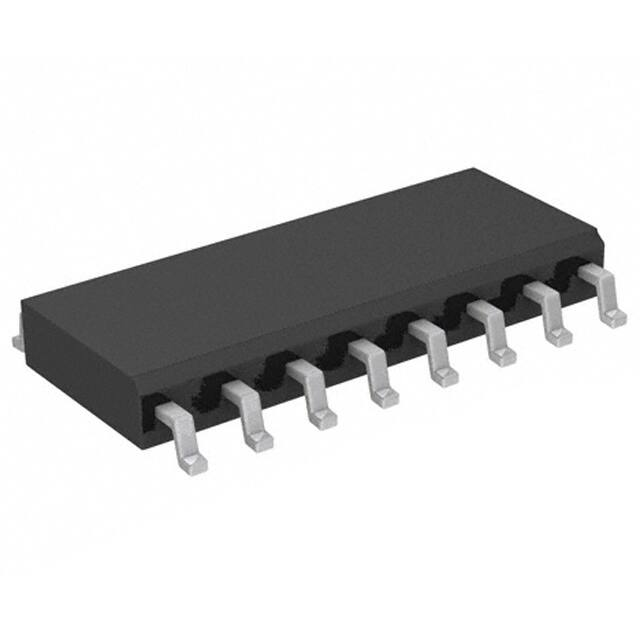
SN55ALS194, SN75ALS194
QUADRUPLE DIFFERENTIAL LINE DRIVERS
SLLS009D – OCTOBER 1985 – REVISED MAY 1995
D
D
D
D
D
D
D
SN55ALS194 . . . J OR W PACKAGE
SN75ALS194 . . . D OR N PACKAGE
(TOP VIEW)
Meet or Exceed the Requirements of ANSI
Standard EIA/TIA-422-B and ITU
Recommendation V.11
Designed to Operate Up to 20 Mbaud
3-State TTL - Compatible Outputs
Single 5-V Supply Operation
High Output Impedance in Power-Off
Condition
Two Pairs of Drivers, Independently
Enabled
Designed as Improved Replacements for
the MC3487
1A
1Y
1Z
1, 2EN
2Z
2Y
2A
GND
description
1
16
2
15
3
14
4
13
5
12
6
11
7
10
8
9
VCC
4A
4Y
4Z
3, 4EN
3Z
3Y
3A
SN55ALS194 . . . FK PACKAGE
(TOP VIEW)
1Y
1A
NC
V CC
4A
These four differential line drivers are designed
for data transmission over twisted-pair or
parallel-wire transmission lines. They meet the
requirements of ANSI Standard EIA/TIA-422-B
and ITU Recommendation V.11 and are
compatible with 3-state TTL circuits. Advanced
low-power Schottky technology provides high
speed without the usual power penalty. Standby
supply current is typically only 26 mA. Typical
propagation delay time is less than 10 ns, and
enable/disable times are typically less than
16 ns.
4
3 2 1 20 19
18
5
17
6
16
7
15
8
14
9 10 11 12 13
4Y
4Z
NC
3, 4EN
3Z
2A
GND
NC
3A
3Y
1Z
1, 2EN
NC
2Z
2Y
High-impedance inputs keep input currents low:
less than 1 µA for a high level and less than
100 µA for a low level. The driver circuits can be
enabled in pairs by separate active-high enable
inputs. The SN55ALS194 and SN75ALS194 are
capable of data rates in excess of 20 megabits
per second and are designed to operate with the
SN55ALS195 and SN75ALS195 quadruple line
receivers.
NC – No internal connection
The SN55ALS194 is characterized for operation over the full military temperature range of – 55°C to 125°C. The
SN75ALS194 is characterized for operation from 0°C to 70°C.
FUNCTION TABLE
(each driver)
OUTPUTS
INPUTS
A
OUTPUT
EN
H
H
H
L
L
H
L
H
X
L
Z
Z
Y
Z
H = high level, L = low level, X = irrelevant,
Z = high impedance
Please be aware that an important notice concerning availability, standard warranty, and use in critical applications of
Texas Instruments semiconductor products and disclaimers thereto appears at the end of this data sheet.
Copyright 1995, Texas Instruments Incorporated
PRODUCTION DATA information is current as of publication date.
Products conform to specifications per the terms of Texas Instruments
standard warranty. Production processing does not necessarily include
testing of all parameters.
POST OFFICE BOX 655303
• DALLAS, TEXAS 75265
1
�SN55ALS194, SN75ALS194
QUADRUPLE DIFFERENTIAL LINE DRIVERS
SLLS009D – OCTOBER 1985 – REVISED MAY 1995
logic symbol†
1, 2EN
4
logic diagram (positive logic)
4
EN
1, 2EN
2
1A
1
3
6
2A
7
5
1Y
2
1A
1Z
12
6
2Z
9
11
14
4A
7
5
1Y
1Z
2Y
2Z
EN
10
3A
3
2Y
2A
3, 4EN
1
15
13
3, 4EN
12
3Y
3Z
10
3A
4Y
9
11
3Y
3Z
4Z
14
† This symbol is in accordance with ANSI/IEEE Std 91-1984 and
IEC Publication 617-12.
Pin numbers shown are for the D, J, N, and W packages.
4A
15
13
4Y
4Z
schematics of inputs and outputs
EQUIVALENT OF EACH
DATA (A) INPUT
VCC
Input
EQUIVALENT OF EACH
ENABLE INPUT
VCC
EQUIVALENT OF EACH
OUTPUT
VCC
Input
Output
2
POST OFFICE BOX 655303
• DALLAS, TEXAS 75265
�SN55ALS194, SN75ALS194
QUADRUPLE DIFFERENTIAL LINE DRIVERS
SLLS009D – OCTOBER 1985 – REVISED MAY 1995
absolute maximum ratings over operating free-air temperature range (unless otherwise noted) †
Supply voltage, VCC (see Note 1) . . . . . . . . . . . . . . . . . . . . . . . . . . . . . . . . . . . . . . . . . . . . . . . . . . . . . . . . . . . . . 7 V
Input voltage, VI . . . . . . . . . . . . . . . . . . . . . . . . . . . . . . . . . . . . . . . . . . . . . . . . . . . . . . . . . . . . . . . . . . . . . . . . . . 5.5 V
Output voltage, VO . . . . . . . . . . . . . . . . . . . . . . . . . . . . . . . . . . . . . . . . . . . . . . . . . . . . . . . . . . . . . . . . . . . . . . . . . 7 V
Continuous total dissipation . . . . . . . . . . . . . . . . . . . . . . . . . . . . . . . . . . . . . . . . . . . See Dissipation Rating Table
Operating free-air temperature range, TA: SN55ALS194 . . . . . . . . . . . . . . . . . . . . . . . . . . . . – 55°C to 125°C
SN75ALS194 . . . . . . . . . . . . . . . . . . . . . . . . . . . . . . . . 0°C to 70°C
Storage temperature range, Tstg . . . . . . . . . . . . . . . . . . . . . . . . . . . . . . . . . . . . . . . . . . . . . . . . . . – 65°C to 150°C
Case temperature for 60 seconds, TC: FK package . . . . . . . . . . . . . . . . . . . . . . . . . . . . . . . . . . . . . . . . . . 260°C
Lead temperature 1,6 mm (1/16 inch) from case for 10 seconds: D, N, or W package . . . . . . . . . . . . . 260°C
Lead temperature 1,6 mm (1/16 inch) from case for 60 seconds: J package . . . . . . . . . . . . . . . . . . . . . 300°C
† Stresses beyond those listed under “absolute maximum ratings” may cause permanent damage to the device. These are stress ratings only, and
functional operation of the device at these or any other conditions beyond those indicated under “recommended operating conditions” is not
implied. Exposure to absolute-maximum-rated conditions for extended periods may affect device reliability.
NOTE 1: All voltage values are with respect to network ground terminal
DISSIPATION RATING TABLE
PACKAGE
TA ≤ 25°C
POWER RATING
DERATING FACTOR
ABOVE TA = 25°C
TA = 70°C
POWER RATING
TA = 125°C
POWER RATING
D
950 mW
7.6 mW/°C
608 mW
N/A
FK
1375 mW
11.0 mW/°C
880 mW
275 mW
J
1375 mW
11.0 mW/°C
880 mW
275 mW
N
1150 mW
9.2 mW/°C
736 mW
N/A
W
1000 mW
8.0 mW/°C
640 mW
200 mW
recommended operating conditions‡
SN55ALS194
Supply voltage, VCC
All inputs, TA = 25°C
High-level input voltage, VIH
A inputs, TA = Full range
EN inputs, TA = Full range
NOM
MAX
MIN
NOM
MAX
4.5
5
5.5
4.75
5
5.25
2
2
2
2
2.1
2
Low-level input voltage, VIL
High-level output current, IOH
Low level output current,
Low-level
current IOL
TA = 25°C
TA = Full range
Operating free-air temperature, TA
– 55
‡ Full range is TA = – 55°C to 125°C for SN55ALS194 and TA = 0°C to 70°C for SN75ALS194.
POST OFFICE BOX 655303
SN75ALS194
MIN
• DALLAS, TEXAS 75265
UNIT
V
V
0.8
0.8
V
– 20
– 20
mA
48
48
20
48
125
0
70
mA
°C
3
�SN55ALS194, SN75ALS194
QUADRUPLE DIFFERENTIAL LINE DRIVERS
SLLS009D – OCTOBER 1985 – REVISED MAY 1995
electrical characteristics over recommended ranges of supply voltage and operating free-air
temperature range (unless otherwise noted)
TEST CONDITIONS†
PARAMETER
VIK
Input clamp voltage
VCC = MIN,
VOH
High level output voltage
High-level
VCC = MIN,,
IOH = –20 mA
VOL
VO
Low-level output voltage
Output voltage
VCC = MIN,
IO = 0
|VOD1|
Differential output voltage
IO = 0
|VOD2|
Differential output voltage
∆|VOD|
Change in magnitude of
differential output voltage¶
VOC
Common-mode output voltage
∆|VOC|
Change in magnitude of
common-mode output voltage¶
IO
Output current with power off
VCC = 0
IOZ
High-impedance-state output current
VCC = MAX
MAX,
Output enables at 0.8 V
II
IIH
Input current at maximum input voltage
IIL
IOS
Low-level input current
High-level input current
Short-circuit output current#
MIN
II = – 18 mA
SN55ALS194
2.4
SN75ALS194
2.5
TYP‡
MAX
UNIT
– 1.5
V
V
IOL = MAX
0.5
V
0
6
V
1.5
6
V
1/2 VOD1
or 2§
RL = 100 Ω,
V
See Figure 1
VO = 6 V
VO = – 0.25 V
± 0.4
V
±3
V
± 0.4
V
100
– 100
VO = 2.7 V
100
VO = 0.5 V
– 100
µA
µA
VCC = MAX,
VCC = MAX,
VI = 5.5 V
VI = 2.7 V
100
µA
50
µA
VCC = MAX,
VCC = MAX,
VI = 0.5 V
VI = 2 V
– 200
µA
– 140
mA
– 40
ICC
Supply current (all drivers)
VCC = MAX,
All outputs disabled
26
45
mA
† For conditions shown as MIN or MAX, use the appropriate value specified under recommended operating conditions.
‡ All typical values are at VCC = 5 V, TA = 25°C.
§ The minimum VOD2 with a 100-Ω load is either 1/2 VOD1 or 2 V, whichever is greater.
¶ ∆ | VOD | and ∆ | VOC | are the changes in magnitude of VOD and VOC, respectively, that occur when the input is changed from a high level to
a low level.
# Not more than one output should be shorted at a time, and duration of the short circuit should not exceed one second.
switching characteristics, VCC = 5 V, TA = 25°C
TEST
CONDITIONS
PARAMETER
tPLH
tPHL
SN55ALS194
MIN
Propagation delay time, low- to high-level output
Propagation delay time, high- to low-level output
F
CL = 15 pF,
See Figure 2
Output-to-output skew
CL = 15 pF,
See Figure 3
SN75ALS194
TYP
MAX
6
9
MIN
UNIT
TYP
MAX
13
6
13
ns
14
9
14
ns
3.5
6
3.5
6
ns
8
14
8
14
ns
tt(OD)
Differential output transition time
tPZH
tPZL
Output enable time to high level
9
12
9
12
ns
Output enable time to low level
12
20
12
20
ns
tPHZ
tPLZ
Output disable time from high level
9
15
9
14
ns
12
15
12
15
ns
4
CL = 15 pF,
See Figure 4
Output disable time from low level
POST OFFICE BOX 655303
• DALLAS, TEXAS 75265
�SN55ALS194, SN75ALS194
QUADRUPLE DIFFERENTIAL LINE DRIVERS
SLLS009D – OCTOBER 1985 – REVISED MAY 1995
SYMBOL EQUIVALENTS
DATA SHEET PARAMETER
EIA/TIA-422-B
VO
| VOD1 |
Voa, Vob
Vo
| VOD2 |
∆ | VOD |
Vt (RL = 100 Ω)
| |Vt| – |Vt| |
VOC
∆ | VOC |
| Vos |
| Vos – Vos |
IOS
IO
|Isa|, |Isb|
|Ixa| , |Ixb|
RL
2
VOD2
RL
2
VOC
Figure 1. Driver VOD and VOC
PARAMETER MEASUREMENT INFORMATION
3V
Input
5V
S1
Generator
(see Note A)
200 Ω
1.5 V
1.5 V
0V
tPHL
tPLH
Y Output
1.5 V
VOH
1.5 V
50 Ω
VOL
CL = 15 pF
(see Note B)
Skew
Skew
tPHL
3V
tPLH
VOH
See Note C
Z Output
1.5 V
1.5 V
VOL
VOLTAGE WAVEFORM
TEST CIRCUIT
NOTES: A. The input pulse is supplied by a generator having the following characteristics: tr ≤ 5 ns, tf ≤ 5 ns, PRR ≤ 1 MHz, duty cycle ≤ 50%,
ZO ≈ 50 Ω .
B. CL includes probe and stray capacitance.
C. All diodes are 1N916 or 1N3064.
Figure 2. Test Circuit and Voltage Waveform
3V
Input
Generator
(see Note A)
CL
RL = 100 Ω
50 Ω
3V
0V
Output
CL
CL = 15 pF
(see Note B)
TEST CIRCUIT
tt(OD)
tt(OD)
90%
Output
10%
VOLTAGE WAVEFORM
NOTES: A. The input pulse is supplied by a generator having the following characteristics: tr ≤ 5 ns, tf ≤ 5 ns, PRR ≤ 1 MHz, duty cycle ≤ 50%,
ZO ≈ 50 Ω .
B. CL includes probe and stray capacitance.
Figure 3. Differential-Output Test Circuit and Voltage Waveform
POST OFFICE BOX 655303
• DALLAS, TEXAS 75265
5
�SN55ALS194, SN75ALS194
QUADRUPLE DIFFERENTIAL LINE DRIVERS
SLLS009D – OCTOBER 1985 – REVISED MAY 1995
PARAMETER MEASUREMENT INFORMATION
5V
Output
S3
200 Ω
S1
0 V or 3 V
Generator
(see Note A)
1 kΩ
CL = 15 pF
(see Note B)
See Note C
50 Ω
S2
TEST CIRCUIT
Output
Enable
Input
3V
1.5 V
0V
tPHZ
Output
S1 Closed
S2 Closed
VOH
0.5 V
≈ 1.5 V
tPLZ
Output
S1 Closed
S2 Closed
1.5 V
≈ 1.5 V
0.5 V
VOL
Output
Enable
Input
0V
3V
1.5 V
tPZL
Output
S1 Closed
S2 Open
1.5 V
VOL
tPZH
Output
S1 Open
S2 Closed
VOH
1.5 V
VOLTAGE WAVEFORMS
NOTES: A. The input pulse is supplied by a generator having the following characteristics: tr ≤ 5 ns, tf ≤ 5 ns, PRR ≤ 1 MHz, duty cycle ≤ 50%,
ZO ≈ 50 Ω .
B. CL includes probe and stray capacitance.
C. All diodes are 1N916 or 1N3064.
Figure 4. Driver Test Circuit and Voltage Waveforms
6
POST OFFICE BOX 655303
• DALLAS, TEXAS 75265
�SN55ALS194, SN75ALS194
QUADRUPLE DIFFERENTIAL LINE DRIVERS
SLLS009D – OCTOBER 1985 – REVISED MAY 1995
TYPICAL CHARACTERISTICS†
Y OUTPUT VOLTAGE
vs
DATA INPUT VOLTAGE
Y OUTPUT VOLTAGE
vs
DATA INPUT VOLTAGE
5
4.5
VCC = 5 V
Outputs Enabled
No Load
4.5
4
VCC = 5.5 V
3.5
VO – Y Output Voltage – V
VO – Y Output Voltage – V
5
No Load
Outputs Enabled
TA = 25°C
VCC = 5 V
VCC = 4.5 V
3
2.5
2
1.5
4
TA = 125°C
3.5
3
TA = 25°C
2.5
TA = 0°C
TA = 70°C
2
TA = – 55°C
1.5
1
1
0.5
0.5
0
0
0
0.5
1
1.5
2
2.5
0
3
0.5
1
VI – Data Input Voltage – V
Figure 5
2
2.5
3
Figure 6
Y OUTPUT VOLTAGE
vs
ENABLE G INPUT VOLTAGE
Y OUTPUT VOLTAGE
vs
ENABLE G INPUT VOLTAGE
4
5
VCC = 5.5 V
VCC = 5 V
VI = 2 V
RL = 470 Ω to GND
See Note A
TA = 125°C
4.5
3.5
VCC = 5 V
VO – Y Output Voltage – V
VO – Y Output Voltage – V
1.5
VI – Data Input Voltage – V
3
VCC = 4.5 V
2.5
2
1.5
4
3.5
3
TA = 25°C
2.5
TA = 0°C
TA = 70°C
2
TA = – 55°C
1.5
1
1
VI = 2 V
RL = 470 Ω to GND
See Note A
TA = 25°C
0.5
0
0
0.5
1
1.5
2
2.5
0.5
0
3
0
0.5
VI – Enable G Input Voltage – V
1
1.5
2
2.5
3
VI – Enable G Input Voltage – V
Figure 8
Figure 7
† Data for temperatures below 0°C and above 70°C are applicable to the SN55ALS194 circuits only.
NOTE A: The A input is connected to VCC during the testing of the Y outputs and to GND during the testing of the Z outputs.
POST OFFICE BOX 655303
• DALLAS, TEXAS 75265
7
�SN55ALS194, SN75ALS194
QUADRUPLE DIFFERENTIAL LINE DRIVERS
SLLS009D – OCTOBER 1985 – REVISED MAY 1995
TYPICAL CHARACTERISTICS†
Z OUTPUT VOLTAGE
vs
ENABLE G INPUT VOLTAGE
6
VCC = 5 V
VCC = 5 V
RL = 470 Ω to VCC
See Note B
5
VCC = 4.5 V
VO – Z Output Voltage – V
VO – Z Output Voltage – V
6
RL = 470 Ω to VCC
TA = 25°C
See Note A
VCC = 5.5 V
5
Z OUTPUT VOLTAGE
vs
ENABLE G INPUT VOLTAGE
4
3
2
1
4
TA = 125°C
TA = 70°C
3
TA = 25°C
TA = 0°C
2
TA = – 55°C
1
0
0
0.5
1
1.5
2
2.5
0
3
0
0.5
VI – Enable G Input Voltage – V
1
5
VOH – High-Level Output Voltage – V
VCC = 5 V
IOH = – 20 mA
See Note A
4
3.5
3
2.5
2
1.5
1
0.5
4.5
TA = 25°C
See Note A
4
3.5
VCC = 5.5 V
3
VCC = 5 V
2.5
VCC = 4.5 V
2
1.5
1
0.5
0
– 50
– 25
0
25
50
75
100
125
TA – Free-Air Temperature – °C
0 – 10 – 20 – 30 – 40 – 50 – 60 – 70 – 80 – 90 – 100
IOH – High-Level Output Current – mA
Figure 11
Figure 12
† Data for temperatures below 0°C and above 70°C are applicable to the SN55ALS194 circuits only.
NOTES: A. The A input is connected to VCC during the testing of the Y outputs and to GND during the testing of the Z outputs.
B. The A input is connected to ground during the testing of the Y outputs and to VCC during the testing of the Z outputs.
8
3
HIGH-LEVEL OUTPUT VOLTAGE
vs
HIGH-LEVEL OUTPUT CURRENT
5
VOH – High-Level Output Voltage – V
2.5
Figure 10
HIGH-LEVEL OUTPUT VOLTAGE
vs
FREE-AIR TEMPERATURE
0
– 75
2
VI – Enable G Input Voltage – V
Figure 9
4.5
1.5
POST OFFICE BOX 655303
• DALLAS, TEXAS 75265
�SN55ALS194, SN75ALS194
QUADRUPLE DIFFERENTIAL LINE DRIVERS
SLLS009D – OCTOBER 1985 – REVISED MAY 1995
TYPICAL CHARACTERISTICS†
LOW-LEVEL OUTPUT VOLTAGE
vs
LOW-LEVEL OUTPUT CURRENT
LOW-LEVEL OUTPUT VOLTAGE
vs
FREE-AIR TEMPERATURE
0.45
1
VCC = 5 V
IOL= – 20 mA
See Note A
VOL – Low-Level Output Voltage – V
VOL – Low-Level Output Voltage – V
0.5
0.4
0.35
0.3
0.25
0.2
0.15
0.1
TA = 25°C
See Note A
0.9
VCC = 4.5 V
0.8
0.7
VCC = 5 V
0.6
0.5
0.4
VCC = 5.5 V
0.3
0.2
0.1
0.05
0
– 75
0
– 50
– 25
0
25
50
75
100
125
0
TA – Free-Air Temperature – °C
10
20
30
40
50
60
70
80
90 100
IOL – Low-Level Output Current – mA
Figure 14
Figure 13
NOTE A: The A input is connected to GND during the testing of the Y outputs and to VCC during the testing of the Z outputs.
SUPPLY CURRENT
vs
SUPPLY VOLTAGE
SUPPLY CURRENT
vs
SUPPLY VOLTAGE
40
80
Outputs Enabled
No Load
TA = 25°C
A Inputs Open or Grounded
Outputs Disabled
No Load
TA = 25°C
35
60
I CC – Supply Current – mA
I CC – Supply Current – mA
70
50
Inputs Grounded
40
Inputs Open
30
20
30
25
20
15
10
5
10
0
0
0
1
2
3
4
5
6
VCC – Supply Voltage – V
7
8
0
1
2
3
4
5
6
7
8
VCC – Supply Voltage – V
Figure 16
Figure 15
† Data for temperatures below 0°C and above 70°C are applicable to the SN55ALS194 circuits only.
POST OFFICE BOX 655303
• DALLAS, TEXAS 75265
9
�SN55ALS194, SN75ALS194
QUADRUPLE DIFFERENTIAL LINE DRIVERS
SLLS009D – OCTOBER 1985 – REVISED MAY 1995
TYPICAL CHARACTERISTICS
SUPPLY CURRENT
vs
FREQUENCY
60
VCC = 5 V
Input = 0 to 3 V
Duty Cycle = 50%
CL = 30 pF to All Outputs
I CC – Supply Current – mA
50
40
30
20
10
0
10 k
100 k
1M
10 M
f – Frequency – Hz
Figure 17
10
POST OFFICE BOX 655303
• DALLAS, TEXAS 75265
100 M
�PACKAGE OPTION ADDENDUM
www.ti.com
14-Oct-2022
PACKAGING INFORMATION
Orderable Device
Status
(1)
Package Type Package Pins Package
Drawing
Qty
Eco Plan
(2)
Lead finish/
Ball material
MSL Peak Temp
Op Temp (°C)
Device Marking
(3)
Samples
(4/5)
(6)
SN75ALS194D
ACTIVE
SOIC
D
16
40
RoHS & Green
NIPDAU
Level-1-260C-UNLIM
0 to 70
75ALS194
Samples
SN75ALS194DR
ACTIVE
SOIC
D
16
2500
RoHS & Green
NIPDAU
Level-1-260C-UNLIM
0 to 70
75ALS194
Samples
SN75ALS194N
ACTIVE
PDIP
N
16
25
RoHS & Green
NIPDAU
N / A for Pkg Type
0 to 70
SN75ALS194N
Samples
SN75ALS194NSR
ACTIVE
SO
NS
16
2000
RoHS & Green
NIPDAU
Level-1-260C-UNLIM
0 to 70
75ALS194
Samples
(1)
The marketing status values are defined as follows:
ACTIVE: Product device recommended for new designs.
LIFEBUY: TI has announced that the device will be discontinued, and a lifetime-buy period is in effect.
NRND: Not recommended for new designs. Device is in production to support existing customers, but TI does not recommend using this part in a new design.
PREVIEW: Device has been announced but is not in production. Samples may or may not be available.
OBSOLETE: TI has discontinued the production of the device.
(2)
RoHS: TI defines "RoHS" to mean semiconductor products that are compliant with the current EU RoHS requirements for all 10 RoHS substances, including the requirement that RoHS substance
do not exceed 0.1% by weight in homogeneous materials. Where designed to be soldered at high temperatures, "RoHS" products are suitable for use in specified lead-free processes. TI may
reference these types of products as "Pb-Free".
RoHS Exempt: TI defines "RoHS Exempt" to mean products that contain lead but are compliant with EU RoHS pursuant to a specific EU RoHS exemption.
Green: TI defines "Green" to mean the content of Chlorine (Cl) and Bromine (Br) based flame retardants meet JS709B low halogen requirements of