���������� ��
�������
���
� ����� ���� ������ ���
�
�
SLLS513A − AUGUST 2001 − REVISED MARCH 2004
D Single-Chip and Single-Supply Interface for
D
D
D
D
D
D
D
D
D
D
D
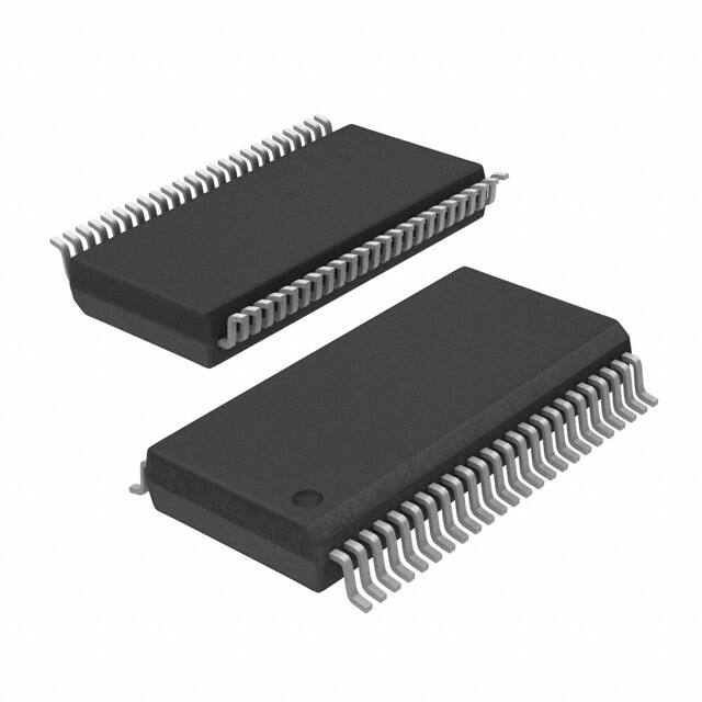
DGG OR DL PACKAGE
(TOP VIEW)
Two IBM PC/AT Serial Ports
Meet or Exceed the Requirements of
TIA/EIA-232-F and ITU v.28 Standards
Operate With 3-V to 5.5-V VCC Supply
Always-Active Noninverting Receiver
Output (ROUT2) Per Port
Operate Up To 250 kbit/s
Low Standby Current . . . 1 µA Typical
External Capacitors . . . 4 × 0.22 µF
Accept 5-V Logic Input With 3.3-V Supply
Allow for Flexible Power Down of Either
Serial Port
Serial-Mouse Driveability
RS-232 Bus-Pin ESD Protection Exceeds
±15 kV Using Human-Body Model (HBM)
Applications
− Battery-Powered Systems, Notebooks,
Laptops, Palmtop PCs, and Hand-Held
Equipment
RIN5A
RIN4A
RIN3A
RIN2A
RIN1A
INVA
DOUT3A
DOUT2A
DOUT1A
FORCEOFFA
C2−
C2+
GND
VCC
FORCEOFFB
DOUT1B
DOUT2B
DOUT3B
INVB
RIN1B
RIN2B
RIN3B
RIN4B
RIN5B
description/ordering information
1
48
2
47
3
46
4
45
5
44
6
43
7
42
8
41
9
40
10
39
11
38
12
37
13
36
14
35
15
34
16
33
17
32
18
31
19
30
20
29
21
28
22
27
ROUT5A
ROUT4A
ROUT3A
ROUT2A
ROUT1A
ROUT2A
DIN3A
DIN2A
DIN1A
FORCEON
V−
V+
C1+
C1−
GND
DIN1B
DIN2B
DIN3B
ROUT2B
ROUT1B
ROUT2B
ROUT3B
ROUT4B
ROUT5B
26
The SN65C23243 and SN75C23243 consist of
24
25
two ports, each containing three line drivers and
five line receivers, and a dual charge-pump circuit
with ±15-kV ESD protection pin to pin (serial-port
connection pins, including GND). These devices meet the requirements of TIA/EIA-232-F and provide the
electrical interface between an asynchronous communication controller and the serial-port connector. This
combination of drivers and receivers matches that needed for two typical serial ports used in an IBM PC/AT, or
compatible. The charge pump and four small external capacitors allow operation from a single 3-V to 5.5-V
supply. In addition, these devices include an always-active noninverting output (ROUT2) per port, which allows
applications using the ring indicator to transmit data while the devices are powered down. The devices operate
at data signaling rates up to 250 kbit/s and a maximum of 30-V/µs driver output slew-rate.
23
ORDERING INFORMATION
−0°C
−0
C to 70
70°C
C
SSOP (DL)
TSSOP (DGG)
−40°C
−40
C to 85
85°C
C
ORDERABLE
PART NUMBER
PACKAGE†
TA
SSOP (DL)
Tube of 25
SN75C23243DL
Reel of 1000
SN75C23243DLR
Reel of 2000
SN75C23243DGGR
Tube of 25
SN65C23243DL
Reel of 1000
SN65C23243DLR
TOP-SIDE
MARKING
75C23243
75C23243
65C23243
TSSOP (DGG)
Reel of 2000
SN65C23243DGGR
65C23243
† Package drawings, standard packing quantities, thermal data, symbolization, and PCB design guidelines are
available at www.ti.com/sc/package.
Please be aware that an important notice concerning availability, standard warranty, and use in critical applications of
Texas Instruments semiconductor products and disclaimers thereto appears at the end of this data sheet.
IBM is a trademark of International Business Machines Corporation.
Copyright 2004, Texas Instruments Incorporated
������
��� ��
� ����������� �! "#��$�� �! �� %#&'�"����� (��$�
���(#"�! "������ �� !%$"���"�����! %$� �)$ �$��! ��
$*�! ��!��#�$��!
!���(��( +������,� ���(#"���� %��"$!!��- (�$! ��� �$"$!!���', ��"'#($
�$!���- �� �'' %����$�$�!�
POST OFFICE BOX 655303
• DALLAS, TEXAS 75265
1
����������� ��
�������
���
� ����� ���� ������ ���
�
�
SLLS513A − AUGUST 2001 − REVISED MARCH 2004
description/ordering information (continued)
Flexible control options for power management are available when either or both serial ports are inactive. The
auto-powerdown feature functions when FORCEON is low and FORCEOFF is high. During this mode of
operation, if the device does not sense a valid RS-232 signal, the driver outputs of its respective port are
disabled. If FORCEOFF is set low, both drivers and receivers (except ROUT2) are shut off, and the supply
current is reduced to 1 µA. Disconnecting the serial port or turning off the peripheral drivers causes the
auto-powerdown condition to occur.
Auto-powerdown can be disabled when FORCEON and FORCEOFF are high and should be done when driving
a serial mouse. With auto-powerdown enabled, the RS-232 port is activated automatically when a valid signal
is applied to any respective receiver input. The INV output is used to notify the user if an RS-232 signal is present
at any receiver input. INV is high (valid data) if any receiver input voltage is greater than 2.7 V or less than −2.7 V
or has been between −0.3 V and 0.3 V for less than 30 µs. INV is low (invalid data) if all receiver input voltages
are between −0.3 V and 0.3 V for more than 30 µs. Refer to Figure 5 for receiver input levels.
Function Tables
EACH DRIVER
(each port)
INPUTS
DIN
FORCEON
FORCEOFF
VALID RIN
RS-232 LEVEL
OUTPUT
DOUT
DRIVER STATUS
X
X
L
X
Z
Powered off
L
H
H
X
H
H
H
H
X
L
Normal operation with
auto-powerdown disabled
L
L
H
Yes
H
H
L
H
Yes
L
L
L
H
No
Z
H
L
H
No
Z
Normal operation with
auto-powerdown enabled
Powered off by
auto-powerdown feature
H = high level, L = low level, X = irrelevant, Z = high impedance
EACH RECEIVER
(each port)
INPUTS
RIN2
RIN1,
RIN3−RIN5
L
OUTPUTS
FORCEOFF
VALID RIN
RS-232 LEVEL
ROUT2
ROUT
X
L
X
L
Z
H
X
L
X
H
Z
L
L
H
Yes
L
H
L
H
H
Yes
L
L
H
L
H
Yes
H
H
H
H
H
Yes
H
L
Open
Open
H
No
L
H
RECEIVER STATUS
Powered off while
ROUT2 is active
Normal operation with
auto-powerdown
disabled/enabled
H = high level, L = low level, X = irrelevant, Z = high impedance (off), Open = input disconnected or connected
driver off
2
POST OFFICE BOX 655303
• DALLAS, TEXAS 75265
����������� ��
�������
���
� ����� ���� ������ ���
�
�
SLLS513A − AUGUST 2001 − REVISED MARCH 2004
logic diagram (positive logic)
RIN5A
RIN4A
RIN3A
RIN2A
RIN1A
1
48
2
47
3
46
4
45
5
44
43
INVA
DOUT3A
DOUT2A
DOUT1A
6
ROUT4A
ROUT3A
ROUT2A
ROUT1A
ROUT2A
Auto-powerdown
7
42
8
41
9
40
39
FORCEOFFA
ROUT5A
DIN3A
DIN2A
DIN1A
FORCEON
10
Charge
Pump
FORCEOFFB
DOUT1B
DOUT2B
DOUT3B
INVB
15
16
33
17
32
18
31
19
RIN2B
RIN3B
RIN4B
RIN5B
DIN2B
DIN3B
Auto-powerdown
30
RIN1B
DIN1B
20
29
21
28
22
27
23
26
24
25
POST OFFICE BOX 655303
• DALLAS, TEXAS 75265
ROUT2B
ROUT1B
ROUT2B
ROUT3B
ROUT4B
ROUT5B
3
����������� ��
�������
���
� ����� ���� ������ ���
�
�
SLLS513A − AUGUST 2001 − REVISED MARCH 2004
timing
Figure 1 shows how the two independent serial ports can be enabled or disabled. As shown by the logic states,
depending on the FORCEOFF, FORCEON, and receiver input levels, either port can be powered down.
Intermediate receiver input levels indicate a 0-V input. Also, it is assumed a pulldown resistor to ground is used
for the receiver outputs. The INV pin goes low when its respective receiver input does not supply a valid RS-232
level. For simplicity, voltage levels, timing differences, and input/output edge rates are not shown.
FORCEOFFA
FORCEOFFB
FORCEON
0V
RIN2A
0V
RIN2B
DINA
DINB
ROUT2A
ROUT2A
ROUT2B
ROUT2B
DOUTA
0V
DOUTB
0V
INVA
INVB
A
NOTES: A.
B.
C.
D.
E.
B
C
D
Ports A and B manually powered off
Port A manually powered off, port B in normal operation with auto-powerdown enabled
Port B powered off by auto-powerdown, port A in normal operation with auto-powerdown enabled
Port A in normal operation with auto-powerdown disabled, port B manually powered off
Ports A and B in normal operation with auto-powerdown disabled
Figure 1. Timing Diagram
4
POST OFFICE BOX 655303
• DALLAS, TEXAS 75265
E
����������� ��
�������
���
� ����� ���� ������ ���
�
�
SLLS513A − AUGUST 2001 − REVISED MARCH 2004
absolute maximum ratings over operating free-air temperature range (unless otherwise noted)†
Supply voltage range, VCC (see Note 1) . . . . . . . . . . . . . . . . . . . . . . . . . . . . . . . . . . . . . . . . . . . . . . −0.3 V to 6 V
Positive output supply voltage range, V+ (see Note 1) . . . . . . . . . . . . . . . . . . . . . . . . . . . . . . . . . . −0.3 V to 7 V
Negative output supply voltage, V− (see Note 1) . . . . . . . . . . . . . . . . . . . . . . . . . . . . . . . . . . . . . . . 0.3 V to −7 V
Supply voltage difference, V+ − V− (see Note 1) . . . . . . . . . . . . . . . . . . . . . . . . . . . . . . . . . . . . . . . . . . . . . . . 13 V
Input voltage range, VI: Driver (FORCEOFF, FORCEON) . . . . . . . . . . . . . . . . . . . . . . . . . . . . . . . −0.3 V to 6 V
Receiver . . . . . . . . . . . . . . . . . . . . . . . . . . . . . . . . . . . . . . . . . . . . . . . . . . . . −25 V to 25 V
Output voltage range, VO: Driver . . . . . . . . . . . . . . . . . . . . . . . . . . . . . . . . . . . . . . . . . . . . . . . . . −13.2 V to 13.2 V
Receiver (INV) . . . . . . . . . . . . . . . . . . . . . . . . . . . . . . . . . . . . . . −0.3 V to VCC + 0.3 V
Package thermal impedance, θJA (see Notes 2 and 3): DGG package . . . . . . . . . . . . . . . . . . . . . . . . . 70°C/W
DL package . . . . . . . . . . . . . . . . . . . . . . . . . . . 63°C/W
Operating virtual junction temperature, TJ . . . . . . . . . . . . . . . . . . . . . . . . . . . . . . . . . . . . . . . . . . . . . . . . . . . 150°C
Storage temperature range, Tstg . . . . . . . . . . . . . . . . . . . . . . . . . . . . . . . . . . . . . . . . . . . . . . . . . . . −65°C to 150°C
† Stresses beyond those listed under “absolute maximum ratings” may cause permanent damage to the device. These are stress ratings only, and
functional operation of the device at these or any other conditions beyond those indicated under “recommended operating conditions” is not
implied. Exposure to absolute-maximum-rated conditions for extended periods may affect device reliability.
NOTES: 1. All voltages are with respect to network GND.
2. Maximum power dissipation is a function of TJ(max), θJA, and TA. The maximum allowable power dissipation at any allowable
ambient temperature is PD = (TJ(max) − TA)/θJA. Operating at the absolute maximum TJ of 150°C can affect reliability.
3. The package thermal impedance is calculated in accordance with JESD 51-7.
recommended operating conditions (see Note 4 and Figure 7)
VCC = 3.3 V
VCC = 5 V
Supply voltage
Driver and control high-level input voltage, VIH
DIN, FORCEOFF, FORCEON
Driver and control low-level input voltage, VIL
DIN, FORCEOFF, FORCEON
Driver and control input voltage, VI
DIN, FORCEOFF, FORCEON
Receiver input voltage, VI
RIN
Operating free-air temperature, TA
VCC = 3.3 V
VCC = 5 V
MIN
NOM
MAX
3
3.3
3.6
4.5
5
5.5
UNIT
V
2
V
2.4
0.8
V
0
5.5
V
V
−25
25
SN75C23243
0
70
SN65C23243
−40
85
°C
NOTE 4: Test conditions are C1−C4 = 0.22 µF at VCC = 3.3 V ± 0.3 V; C1 = 0.047 µF, C2−C4 = 0.33 µF at VCC = 5 V ± 0.5 V.
electrical characteristics over recommended ranges of supply voltage and operating free-air
temperature (unless otherwise noted) (see Note 4 and Figure 7)
PARAMETER
II
ICC
Input leakage current
Supply current
(TA = 25
25°C)
C)
TEST CONDITIONS
FORCEOFF, FORCEON
MIN
TYP‡
MAX
±0.01
±1
µA
0.6
2
mA
Auto-powerdown disabled
No load,
FORCEOFF and FORCEON at VCC
Powered off
No load, FORCEOFF at GND
1
20
Auto-powerdown enabled
No load, FORCEOFF at VCC,
FORCEON at GND,
All RIN are open or grounded
1
20
UNIT
µA
‡ All typical values are at VCC = 3.3 V or VCC = 5 V and TA = 25°C.
NOTE 4: Test conditions are C1−C4 = 0.22 µF at VCC = 3.3 V ± 0.3 V; C1 = 0.047 µF, C2−C4 = 0.33 µF at VCC = 5 V ± 0.5 V.
POST OFFICE BOX 655303
• DALLAS, TEXAS 75265
5
����������� ��
�������
���
� ����� ���� ������ ���
�
�
SLLS513A − AUGUST 2001 − REVISED MARCH 2004
DRIVER SECTION
electrical characteristics over recommended ranges of supply voltage and operating free-air
temperature (unless otherwise noted) (see Note 4 and Figure 7)
PARAMETER
VOH
VOL
VO
IIH
IIL
TEST CONDITIONS
MIN
TYP†
MAX
UNIT
High-level output voltage
All DOUT at RL = 3 kΩ to GND
5
5.4
V
Low-level output voltage
All DOUT at RL = 3 kΩ to GND
−5
−5.4
V
Output voltage
(mouse driveability)
DIN1 = DIN2 = GND, DIN3 = VCC,
3-kΩ to GND at DOUT3, DOUT1 = DOUT2 = −2.5 mA
±5
High-level input current
VI = VCC
VI at GND
Low-level input current
IOS
Short-circuit output current‡
VCC = 3.6 V,
VCC = 5.5 V,
ro
Output resistance
VCC, V+, and V− = 0 V,
VO = 0 V
VO = 0 V
VO = ±2 V
VO = ±12 V,
300
V
±0.01
±1
µA
±0.01
±1
µA
±35
±60
mA
Ω
10M
±25
VCC = 3 V to 3.6 V
µA
VO = ±10 V,
VCC = 4.5 V to 5.5 V
±25
† All typical values are at VCC = 3.3 V or VCC = 5 V and TA = 25°C.
‡ Short-circuit durations should be controlled to prevent exceeding the device absolute power dissipation ratings, and not more than one output
should be shorted at a time.
NOTE 4: Test conditions are C1−C4 = 0.22 µF at VCC = 3.3 V ± 0.3 V; C1 = 0.047 µF, C2−C4 = 0.33 µF at VCC = 5 V ± 0.5 V.
Ioff
Output leakage current
FORCEOFF = GND
switching characteristics over recommended ranges of supply voltage and operating free-air
temperature (unless otherwise noted) (see Note 4 and Figure 7)
PARAMETER
TEST CONDITIONS
Maximum data rate
CL = 1000 pF,
One DOUT switching,
RL = 3 kΩ,
See Figure 1
tsk(p)
Pulse skew§
CL = 150 pF to 2500 pF
RL = 3 kΩ to 7 kΩ,
See Figure 2
SR(tr)
Slew rate, transition region
(see Figure 1)
VCC = 3.3 V,
RL = 3 kΩ to 7 kΩ
MIN
TYP†
MAX
250
kbit/s
100
POST OFFICE BOX 655303
ns
CL = 150 pF to 1000 pF
6
30
CL = 150 pF to 2500 pF
4
30
† All typical values are at VCC = 3.3 V or VCC = 5 V and TA = 25°C.
§ Pulse skew is defined as |tPLH − tPHL| of each channel of the same device.
NOTE 4: Test conditions are C1−C4 = 0.22 µF at VCC = 3.3 V ± 0.3 V; C1 = 0.047 µF, C2−C4 = 0.33 µF at VCC = 5 V ± 0.5 V.
6
• DALLAS, TEXAS 75265
UNIT
V/µs
����������� ��
�������
���
� ����� ���� ������ ���
�
�
SLLS513A − AUGUST 2001 − REVISED MARCH 2004
RECEIVER SECTION
electrical characteristics over recommended ranges of supply voltage and operating free-air
temperature (unless otherwise noted) (see Note 4 and Figure 7)
PARAMETER
VOH
VOL
MIN
TYP†
VCC − 0.6 V
VCC − 0.1 V
TEST CONDITIONS
High-level output voltage
IOH = −1 mA
IOL = 1.6 mA
Low-level output voltage
VIT+
Positive-going input threshold voltage
VCC = 3.3 V
VCC = 5 V
VIT−
Negative-going input threshold voltage
VCC = 3.3 V
VCC = 5 V
Vhys
Ioff
Input hysteresis (VIT+ − VIT−)
MAX
V
0.4
1.6
2.4
1.9
2.4
0.6
1.1
0.8
1.4
FORCEOFF = 0 V
V
V
V
0.5
Output leakage current (except ROUT2B)
UNIT
V
±0.05
ri
Input resistance
VI = ±3 V to ±25 V
3
5
† All typical values are at VCC = 3.3 V or VCC = 5 V and TA = 25°C.
NOTE 4: Test conditions are C1−C4 = 0.22 µF at VCC = 3.3 V ± 0.3 V; C1 = 0.047 µF, C2−C4 = 0.33 µF at VCC = 5 V ± 0.5 V.
±10
µA
7
kΩ
switching characteristics over recommended ranges of supply voltage and operating free-air
temperature (unless otherwise noted) (see Note 4 and Figure 7)
PARAMETER
TEST CONDITIONS
tPLH
tPHL
Propagation delay time, low- to high-level output
ten
tdis
Output enable time
Propagation delay time, high- to low-level output
Output disable time
Pulse skew‡
CL = 150 pF, See Figure 4
CL = 150 pF, RL = 3 kΩ,
kΩ See Figure 5
MIN
TYP†
MAX
150
ns
150
ns
200
ns
200
ns
tsk(p)
See Figure 4
50
† All typical values are at VCC = 3.3 V or VCC = 5 V and TA = 25°C.
‡ Pulse skew is defined as |tPLH − tPHL| of each channel of the same device.
NOTE 4: Test conditions are C1−C4 = 0.22 µF at VCC = 3.3 V ± 0.3 V; C1 = 0.047 µF, C2−C4 = 0.33 µF at VCC = 5 V ± 0.5 V.
POST OFFICE BOX 655303
• DALLAS, TEXAS 75265
UNIT
ns
7
����������� ��
�������
���
� ����� ���� ������ ���
�
�
SLLS513A − AUGUST 2001 − REVISED MARCH 2004
AUTO-POWERDOWN SECTION
electrical characteristics over recommended ranges of supply voltage and operating free-air
temperature (unless otherwise noted) (see Figure 6)
PARAMETER
TEST CONDITIONS
MIN
VT+(valid)
Receiver input threshold
for INV high-level output voltage
FORCEON = GND,
FORCEOFF = VCC
VT−(valid)
Receiver input threshold
for INV high-level output voltage
FORCEON = GND,
FORCEOFF = VCC
−2.7
VT(invalid)
Receiver input threshold
for INV low-level output voltage
FORCEON = GND,
FORCEOFF = VCC
−0.3
VOH
INV high-level output voltage
IOH = −1 mA, FORCEON = GND,
FORCEOFF = VCC
VOL
INV low-level output voltage
IOL = 1.6 mA, FORCEON = GND,
FORCEOFF = VCC
MAX
UNIT
2.7
V
V
0.3
VCC − 0.6
V
V
0.4
V
switching characteristics over recommended ranges of supply voltage and operating free-air
temperature (unless otherwise noted) (see Figure 6)
PARAMETER
tvalid
tinvalid
MIN
MAX
UNIT
Propagation delay time, low- to high-level output
1
µs
Propagation delay time, high- to low-level output
30
µs
100
µs
ten
Supply enable time
† All typical values are at VCC = 3.3 V or VCC = 5 V and TA = 25°C.
8
TYP†
POST OFFICE BOX 655303
• DALLAS, TEXAS 75265
����������� ��
�������
���
� ����� ���� ������ ���
�
�
SLLS513A − AUGUST 2001 − REVISED MARCH 2004
PARAMETER MEASUREMENT INFORMATION
3V
Generator
(see Note B)
Input
RS-232
Output
50 Ω
RL
CL
(see Note A)
3V
FORCEOFF
TEST CIRCUIT
0V
tTHL
Output
6V
SR(tr) +
t THL or t TLH
tTLH
VOH
3V
3V
−3 V
−3 V
VOL
VOLTAGE WAVEFORMS
NOTES: A. CL includes probe and jig capacitance.
B. The pulse generator has the following characteristics: PRR = 250 kbit/s, ZO = 50 Ω, 50% duty cycle, tr ≤ 10 ns, tf ≤ 10 ns.
Figure 2. Driver Slew Rate
3V
Generator
(see Note B)
RS-232
Output
50 Ω
RL
Input
1.5 V
1.5 V
0V
CL
(see Note A)
tPHL
tPLH
VOH
3V
FORCEOFF
50%
50%
Output
VOL
TEST CIRCUIT
VOLTAGE WAVEFORMS
NOTES: A. CL includes probe and jig capacitance.
B. The pulse generator has the following characteristics: PRR = 250 kbit/s, ZO = 50 Ω, 50% duty cycle, tr ≤ 10 ns, tf ≤ 10 ns.
Figure 3. Driver Pulse Skew
3 V or 0 V
FORCEON
3V
Input
1.5 V
1.5 V
−3 V
Output
Generator
(see Note B)
50 Ω
3V
FORCEOFF
tPHL
CL
(see Note A)
tPLH
VOH
50%
Output
50%
VOL
TEST CIRCUIT
VOLTAGE WAVEFORMS
NOTES: A. CL includes probe and jig capacitance.
B. The pulse generator has the following characteristics: ZO = 50 Ω, 50% duty cycle, tr ≤ 10 ns, tf ≤ 10 ns.
Figure 4. Receiver Propagation Delay Times
POST OFFICE BOX 655303
• DALLAS, TEXAS 75265
9
����������� ��
�������
���
� ����� ���� ������ ���
�
�
SLLS513A − AUGUST 2001 − REVISED MARCH 2004
PARAMETER MEASUREMENT INFORMATION
3V
Input
3 V or 0 V
FORCEON
VCC
S1
1.5 V
GND
−3 V
tPZH
(S1 at GND)
tPHZ
(S1 at GND)
RL
3 V or 0 V
1.5 V
VOH
Output
50%
Output
CL
(see Note A)
FORCEOFF
Generator
(see Note B)
50 Ω
0.3 V
tPZL
(S1 at VCC)
tPLZ
(S1 at VCC)
0.3 V
Output
50%
VOL
TEST CIRCUIT
NOTES: A.
B.
C.
D.
VOLTAGE WAVEFORMS
CL includes probe and jig capacitance.
The pulse generator has the following characteristics: ZO = 50 Ω, 50% duty cycle, tr ≤ 10 ns, tf ≤ 10 ns.
tPLZ and tPHZ are the same as tdis.
tPZL and tPZH are the same as ten.
Figure 5. Receiver Enable and Disable Times
10
POST OFFICE BOX 655303
• DALLAS, TEXAS 75265
����������� ��
�������
���
� ����� ���� ������ ���
�
�
SLLS513A − AUGUST 2001 − REVISED MARCH 2004
PARAMETER MEASUREMENT INFORMATION
2.7 V
2.7 V
0V
Receiver
Input
0V
50 Ω
tvalid
50% VCC
50% VCC
0V
ten
INV
CL = 30 pF
(see Note A)
≈V+
V+
0.3 V
VCC
0V
0.3 V
Supply
Voltages
FORCEOFF
FORCEON
tinvalid
DIN
−3 V
VCC
INV
Output
Autopowerdown
−2.7 V
−2.7 V
ROUT
Generator
(see Note B)
3V
DOUT
≈V−
V−
TEST CIRCUIT
VOLTAGE WAVEFORMS
Valid RS-232 Level, INV High
ÎÎÎÎÎÎÎÎÎÎÎÎ
ÎÎÎÎÎÎÎÎÎÎÎÎ
ÎÎÎÎÎÎÎÎÎÎÎÎ
ÎÎÎÎÎÎÎÎÎÎÎÎ
ÎÎÎÎÎÎÎÎÎÎÎÎ
2.7 V
Indeterminate
0.3 V
0V
If Signal Remains Within This Region
for More Than 30 µs, INV Is Low†
−0.3 V
Indeterminate
−2.7 V
Valid RS-232 Level, INV High
† Auto-powerdown disables drivers and reduces
supply current to 1 µA.
NOTES: A. CL includes probe and jig capacitance.
B. The pulse generator has the following characteristics: PRR = 5 kbit/s, ZO = 50 Ω, 50% duty cycle, tr ≤ 10 ns, tf ≤ 10 ns.
Figure 6. INV Propagation Delay Times and Supply Enabling Time
POST OFFICE BOX 655303
• DALLAS, TEXAS 75265
11
����������� ��
�������
���
� ����� ���� ������ ���
�
�
SLLS513A − AUGUST 2001 − REVISED MARCH 2004
APPLICATION INFORMATION
36
C1+
12
+
C2
−
11
38
GND
13, 34
RIN3
RIN4
RIN5
DOUT1
DOUT2
C3†
+ CBYPASS
− = 0.1 µF
+
−
C1
35
C1−
RIN2
RS-232 Outputs
V−
−
14
VCC
+
RIN1
RS-232 Inputs
C2−
+
5 (20)
39
FORCEON
4 (21)
Autopowerdown
C4
−
37
V+
C2+
3 (22)
2 (23)
10 (15)
FORCEOFF
1 (24)
6 (19)
9 (16)
43 (30)
8 (17)
44 (29)
INV
ROUT2
ROUT1
5 kΩ
DOUT3
7 (18)
45 (28)
ROUT2
5 kΩ
DIN3
42 (31)
Logic Outputs
46 (27)
ROUT3
5 kΩ
Logic Inputs
DIN2
41 (32)
47 (26)
ROUT4
5 kΩ
DIN1
40 (33)
48 (25)
ROUT5
5 kΩ
† C3 can be connected to VCC or GND.
NOTES: A. Resistor values shown are nominal.
B. Numbers in parentheses are for B section.
VCC vs CAPACITOR VALUES
VCC
C1
C2, C3, and C4
3.3 V ± 0.3 V
5 V ± 0.5 V
3 V to 5.5 V
0.22 µF
0.047 µF
0.22 µF
0.22 µF
0.33 µF
1 µF
Figure 7. Typical Operating Circuit and Capacitor Values
12
POST OFFICE BOX 655303
• DALLAS, TEXAS 75265
�PACKAGE OPTION ADDENDUM
www.ti.com
23-Apr-2022
PACKAGING INFORMATION
Orderable Device
Status
(1)
Package Type Package Pins Package
Drawing
Qty
Eco Plan
(2)
Lead finish/
Ball material
MSL Peak Temp
Op Temp (°C)
Device Marking
(3)
(4/5)
(6)
SN65C23243DGGR
ACTIVE
TSSOP
DGG
48
2000
RoHS & Green
NIPDAU
Level-1-260C-UNLIM
-40 to 85
65C23243
SN65C23243DLR
ACTIVE
SSOP
DL
48
1000
RoHS & Green
NIPDAU
Level-1-260C-UNLIM
-40 to 85
65C23243
SN75C23243CDGGR
PREVIEW
TSSOP
DGG
48
2000
TBD
Call TI
Call TI
SN75C23243CDLR
PREVIEW
SSOP
DL
48
1000
TBD
Call TI
Call TI
SN75C23243DGGR
ACTIVE
TSSOP
DGG
48
2000
RoHS & Green
NIPDAU
Level-1-260C-UNLIM
0 to 70
75C23243
SN75C23243DLR
ACTIVE
SSOP
DL
48
1000
RoHS & Green
NIPDAU
Level-1-260C-UNLIM
0 to 70
75C23243
(1)
The marketing status values are defined as follows:
ACTIVE: Product device recommended for new designs.
LIFEBUY: TI has announced that the device will be discontinued, and a lifetime-buy period is in effect.
NRND: Not recommended for new designs. Device is in production to support existing customers, but TI does not recommend using this part in a new design.
PREVIEW: Device has been announced but is not in production. Samples may or may not be available.
OBSOLETE: TI has discontinued the production of the device.
(2)
RoHS: TI defines "RoHS" to mean semiconductor products that are compliant with the current EU RoHS requirements for all 10 RoHS substances, including the requirement that RoHS substance
do not exceed 0.1% by weight in homogeneous materials. Where designed to be soldered at high temperatures, "RoHS" products are suitable for use in specified lead-free processes. TI may
reference these types of products as "Pb-Free".
RoHS Exempt: TI defines "RoHS Exempt" to mean products that contain lead but are compliant with EU RoHS pursuant to a specific EU RoHS exemption.
Green: TI defines "Green" to mean the content of Chlorine (Cl) and Bromine (Br) based flame retardants meet JS709B low halogen requirements of