SN75LV4737A
3.3-V/5-V MULTICHANNEL RS-232 LINE DRIVER/RECEIVER
SLLS178D – APRIL 1994 – REVISED FEBRUARY 2000
D
D
D
D
D
D
D
D
D
D
D
DB PACKAGE†
(TOP VIEW)
Single-Chip and Single-Supply Interface for
IBM PC/AT Serial Port
Meets or Exceeds the Requirements of
TIA/EIA-232-F and ITU v.11 Standards
Operates With 3.3-V or 5-V Supplies
One Receiver Remains Active During
Standby (Wake-up Mode)
Designed to Operate at 128 kbit/s Over a
3-m Cable
Low Standby Current . . . 5 µA Max
ESD Protection on RS-232 Pins Meets or
Exceeds 4 kV (HBM) and 1.5 kV (HBM) on
All Pins Per MIL-STD-883, Method 3015
External Capacitors . . . 0.1 µF
(VCC = 3.3 V . . . Five External Capacitors)
(VCC = 5 V . . . Four External Capacitors)
Accepts 5-V Logic Input With 3.3-V Supply
Applications
– RS-232 Interface
– Battery-Powered Systems, PDAs
– Notebook, Laptop, and Palmtop PCs
– External Modems and Hand-Held
Terminals
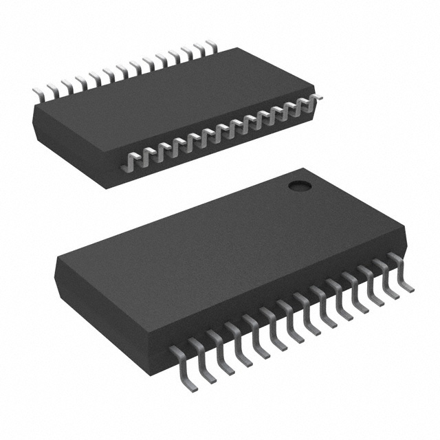
Packaged in Shrink Small-Outline Package
VDD
C2+
VCC
C2–
EN
C1+
DIN1
DIN2
DIN3
ROUT1
ROUT2
ROUT3
ROUT4
ROUT5
1
28
2
27
3
26
4
25
5
24
6
23
7
22
8
21
9
20
10
19
11
18
12
17
13
16
14
15
C3+
GND
C3–
VSS
C1–
STBY
DOUT1
DOUT2
DOUT3
RIN1
RIN2
RIN3
RIN4
RIN5
† The DB package is only
available in left-ended tape and
reel
(order
part
number
SN75LV4737ADBR).
description
The SN75LV4737A‡ consists of three line drivers, five line receivers, and a charge-pump circuit. It provides the
electrical interface between an asynchronous communication controller and the serial-port connector, and
meets the requirements of TIA/EIA-232-F. This combination of drivers and receivers matches those needed for
the typical serial port used in an IBM PC/AT or compatibles. The charge pump and five small external capacitors
allow operation from a single 3.3-V supply, and four capacitors allow operation from a 5-V supply.
The device has flexible control options for power management when the serial port is inactive. A common
disable for all of the drivers and receivers is provided with the active-high STBY input. The active-low EN input
is an enable for one receiver to implement a wake-up feature for the serial port. All the logic inputs can accept
signals from controllers operating from a 5-V supply, even though the SN75LV4737A is operating from 3.3 V.
The SN75LV4737A is characterized for operation over the temperature range of 0°C to 70°C.
Please be aware that an important notice concerning availability, standard warranty, and use in critical applications of
Texas Instruments semiconductor products and disclaimers thereto appears at the end of this data sheet.
‡ Patent-pending design
IBM and PC/AT are trademarks of International Business Machines Corporation.
Copyright 2000, Texas Instruments Incorporated
PRODUCTION DATA information is current as of publication date.
Products conform to specifications per the terms of Texas Instruments
standard warranty. Production processing does not necessarily include
testing of all parameters.
POST OFFICE BOX 655303
• DALLAS, TEXAS 75265
1
�SN75LV4737A
3.3-V/5-V MULTICHANNEL RS-232 LINE DRIVER/RECEIVER
SLLS178D – APRIL 1994 – REVISED FEBRUARY 2000
Function Tables
EACH DRIVER
INPUTS
DIN
STBY
OUTPUT
DOUT
X
H
Z
H
L
L
H
L
L
Open
L
L
H = high level, L = low level,
X = irrelevant, Z = high
impedance
EACH RECEIVER
INPUTS
STBY
EN
RIN5
H
H
H
L
H
L
L
L
X
L
X
OUTPUTS
RIN1–RIN4
ROUT5
ROUT1–ROUT4
X
X
Z
Z
H
X
L
Z
X
H
Z
L
L
H
H
H
H
L
L
H = high level, L = low level, X = irrelevant, Z = high impedance
2
POST OFFICE BOX 655303
• DALLAS, TEXAS 75265
�SN75LV4737A
3.3-V/5-V MULTICHANNEL RS-232 LINE DRIVER/RECEIVER
SLLS178D – APRIL 1994 – REVISED FEBRUARY 2000
logic diagram (positive logic)
DIN1
DIN2
DIN3
RIN1
RIN2
RIN3
RIN4
RIN5
STBY
EN
7
22
8
21
9
20
19
10
18
11
17
12
16
13
15
14
DOUT1
DOUT2
DOUT3
ROUT1
ROUT2
ROUT3
ROUT4
ROUT5
23
5
POST OFFICE BOX 655303
• DALLAS, TEXAS 75265
3
�SN75LV4737A
3.3-V/5-V MULTICHANNEL RS-232 LINE DRIVER/RECEIVER
SLLS178D – APRIL 1994 – REVISED FEBRUARY 2000
schematics of inputs and outputs
STBY AND EN INPUTS
TYPICAL RECEIVER INPUTS
VCC
VCC
Input
Input
VSS
5 kΩ
GND
GND
TYPICAL DRIVER INPUTS
TYPICAL OF ALL
RECEIVER OUTPUTS
TYPICAL OF ALL DRIVER OUTPUTS
VCC
VDD
VCC
Input
Output
Output
300 Ω
GND
VSS
VSS
GND
GND
absolute maximum ratings over operating free-air temperature range (unless otherwise noted)†
Supply voltage, VCC . . . . . . . . . . . . . . . . . . . . . . . . . . . . . . . . . . . . . . . . . . . . . . . . . . . . . . . . . . . . . . . . . . . . . . . . 7 V
Positive output supply voltage, VDD (see Note 1) . . . . . . . . . . . . . . . . . . . . . . . . . . . . . . . . . . . . . . . . . . . . . . . 15 V
Negative output supply voltage, VSS . . . . . . . . . . . . . . . . . . . . . . . . . . . . . . . . . . . . . . . . . . . . . . . . . . . . . . . –15 V
Input voltage range, VI: Driver . . . . . . . . . . . . . . . . . . . . . . . . . . . . . . . . . . . . . . . . . . . . . . . . . . . . . . . . . –3 V to 7 V
Receiver . . . . . . . . . . . . . . . . . . . . . . . . . . . . . . . . . . . . . . . . . . . . . . . . . . . . –30 V to 30 V
Output voltage range, VO: Driver . . . . . . . . . . . . . . . . . . . . . . . . . . . . . . . . . . . . . . . . VSS – 0.3 V to VDD + 0.3 V
Receiver . . . . . . . . . . . . . . . . . . . . . . . . . . . . . . . . . . . . . . . . . . . . . . . . . . –0.3 V to 7 V
Package thermal impedance, θJA (see Note 2) . . . . . . . . . . . . . . . . . . . . . . . . . . . . . . . . . . . . . . . . . . . . . 62°C/W
Lead temperature 1,6 mm (1/16 inch) from case for 10 seconds . . . . . . . . . . . . . . . . . . . . . . . . . . . . . . . 260°C
Storage temperature range, Tstg . . . . . . . . . . . . . . . . . . . . . . . . . . . . . . . . . . . . . . . . . . . . . . . . . . . –65°C to 150°C
† Stresses beyond those listed under “absolute maximum ratings” may cause permanent damage to the device. These are stress ratings only, and
functional operation of the device at these or any other conditions beyond those indicated under “recommended operating conditions” is not
implied. Exposure to absolute-maximum-rated conditions for extended periods may affect device reliability.
NOTES: 1. All voltages are with respect to network GND.
2. The package thermal impedance is calculated in accordance with JESD 51.
4
POST OFFICE BOX 655303
• DALLAS, TEXAS 75265
�SN75LV4737A
3.3-V/5-V MULTICHANNEL RS-232 LINE DRIVER/RECEIVER
SLLS178D – APRIL 1994 – REVISED FEBRUARY 2000
recommended operating conditions
VCC
Supply voltage
DIN, EN, STBY
VIH
Driver high-level input voltage
DIN
VIL
VI
Driver low-level input voltage
NOM
MAX
3
3.3
3.6
V
4.5
5
5.5
V
VCC = 3.3 V
2
2.5
DIN, EN, STBY
Receiver input voltage
3.3-V operation (C1, C2, C3, C4, C5),
5-V operation (C1, C3, C4, C5),
See Note 3 and Figures 6 and 7
External capacitor
UNIT
V
2
VCC = 5 V
EN, STBY
MIN
VCC = 3.3 V
VCC = 5 V
0.8
V
±30
V
µF
0.1
TA
Operating free-air temperature
NOTE 3: C2 is needed only for 3.3-V operation.
0
70
°C
electrical characteristics over recommended ranges of supply voltage and operating free-air
temperature (see Figures 6 and 7) (unless otherwise noted)
PARAMETER
TEST CONDITIONS
VDD
VSS
Positive supply voltage
No load
Negative supply voltage
No load
II
Input current (EN, STBY)
See Notes 4 and 5
ICC
Supply current (standby mode)
(see Note 4)
Supply current (wake-up mode)
(see Note 5)
8
No load,
Inputs open
10
–9.5
VCC = 5 V
TYP†
MAX
MIN
7
–7
8.7
–8
±2
STBY at GND,
EN at VCC or GND
Supply current
VCC = 3.3 V
TYP†
MAX
MIN
8.4
EN, STBY at VCC
EN at GND,
STBY at VCC
10
18
10
12
UNIT
V
–6
V
±2
µA
20.7
mA
5
5
10
10
µA
† All typical values are at VCC = 3.3 V or VCC = 5 V, and TA = 25°C.
NOTES: 4. When standby mode is not used, STBY input must be taken low.
5. When wake-up mode is not used, EN input must be taken high.
POST OFFICE BOX 655303
• DALLAS, TEXAS 75265
5
�SN75LV4737A
3.3-V/5-V MULTICHANNEL RS-232 LINE DRIVER/RECEIVER
SLLS178D – APRIL 1994 – REVISED FEBRUARY 2000
DRIVER SECTION
electrical characteristics over recommended ranges of supply voltage and operating free-air
temperature (unless otherwise noted)
PARAMETER
TEST CONDITIONS
VOH
VOL
High-level output voltage
RL = 3 kΩ
Low-level output voltage
RL = 3 kΩ
IIH
IIL
High-level input current
VI = VCC
VI at GND
IOS
Low-level input current
Short circuit output current (see Note 6)
Short-circuit
MIN
5.5
TYP†
7
–6
VCC = 3.6 V,
VCC = 5.5 V,
VO = 0 V
VO = 0 V
MAX
±15
UNIT
V
–5
V
1
µA
–10
µA
±40
mA
ro
Output resistance
VCC = VDD = VSS = 0 V,
VO = ±2 V
300
500
Ω
† All typical values are at VCC = 3.3 V or VCC = 5 V, and TA = 25°C.
NOTE 6: Short-circuit durations should be controlled to prevent exceeding the device absolute maximum power dissipation ratings, and not more
than one output should be shorted at a time.
switching characteristics over recommended ranges of supply voltage and operating free-air
temperature (unless otherwise noted)
PARAMETER
MIN
TYP†
MAX
VCC = 3.3 V
VCC = 5 V
100
500
850
100
500
850
VCC = 3.3 V
VCC = 5 V
100
500
850
100
500
850
1
5
ms
3
7
ms
VCC = 3.3 V
VCC = 5 V
0.9
3
0.6
3
VCC = 3.3 V
VCC = 5 V
0.5
3
0.3
3
TEST CONDITIONS
tPLH
Propagation delay time,
time lowlow to high-level
high level output
tPHL
time highhigh to low-level
low level output
Propagation delay time,
tPZH
tPZL
Output enable time to high level
tPHZ
Output disable time from high level
tPLZ
Output disable time from low level
SR
Slew rate
CL = 50 pF,
See Figure 1
RL = 3 kΩ to 7 kΩ,
4
30
V/µs
SR(tr)
Slew rate, transition region
CL = 2500 pF,
See Figure 3
RL = 3 kΩ to 7 kΩ,
3
30
V/µs
Output enable time to low level
CL = 50 pF,
RL = 3 kΩ to 7 kΩ
kΩ,
See Figure 1
CL = 50 pF,,
See Figure 2
CL = 50 pF,
RL = 3 kΩ to 7 kΩ
kΩ,
See Figure 2
RL = 3 kΩ to 7 kΩ,,
† All typical values are at VCC = 3.3 V or VCC = 5 V, and TA = 25°C.
6
UNIT
POST OFFICE BOX 655303
• DALLAS, TEXAS 75265
ns
ns
µs
µs
�SN75LV4737A
3.3-V/5-V MULTICHANNEL RS-232 LINE DRIVER/RECEIVER
SLLS178D – APRIL 1994 – REVISED FEBRUARY 2000
RECEIVER SECTION
electrical characteristics over recommended ranges of supply voltage and operating free-air
temperature (unless otherwise noted)
PARAMETER
TEST CONDITIONS
VCC = 3.3 V
VCC = 5 V
MIN
TYP†
2.4
3
3.5
5
MAX
UNIT
VOH
High level output voltage
High-level
2 mA
IOH = –2
VOL
VIT+
Low-level output voltage
IOL = 2 mA
VIT–
Vhys
Negative-going input threshold voltage
0.6
1
Input hysteresis (VIT+ – VIT–)
0.5
1.2
1.8
V
3
5
7
kΩ
Positive-going input threshold voltage
ri
Input resistance
VI = ±3 V to ±25 V
† All typical values are at VCC = 3.3 V or VCC = 5 V, and TA = 25°C.
V
0.2
0.4
V
2.2
2.6
V
V
switching characteristics over recommended ranges of supply voltage and operating free-air
temperature, CL = 50 pF, RL = 3 kΩ to GND
TEST
CONDITIONS
PARAMETER
tPLH
tPHL
VCC = 3.3 V
TYP
MAX
MIN
VCC = 5 V
TYP
MAX
MIN
UNIT
Propagation delay time, low- to high-level output
10
70
200
10
70
200
ns
Propagation delay time, high- to low-level output
10
60
200
10
55
200
ns
40
200
40
200
µs
90
500
70
500
ns
tPLH
Propagation delay time, low- to high-level output
(wake-up mode)
tPHL
Propagation delay time, high- to low-level output
(wake-up mode)
tPZH
tPZL
Output enable time to high level
tPHZ
tPLZ
Output disable time from high level
Output enable time to low level
See Figure 4
See Figure 5
100
Output disable time from low level
POST OFFICE BOX 655303
• DALLAS, TEXAS 75265
3
10
1.2
10
µs
100
250
60
250
ns
200
600
150
600
ns
130
250
60
250
ns
100
7
�SN75LV4737A
3.3-V/5-V MULTICHANNEL RS-232 LINE DRIVER/RECEIVER
SLLS178D – APRIL 1994 – REVISED FEBRUARY 2000
PARAMETER MEASUREMENT INFORMATION
3V
Input
Generator
(see Note B)
tPHL
CL = 50 pF
(see Note A)
RL
50%
5 µs
RS-232
Output
50 Ω
50%
tPLH
tTHL
0V
STBY
tTLH
VOH
90%
90%
Output
10%
10%
TEST CIRCUIT
SR
ǒ
+ 0.8 V Vt * V
OH
OL
0V
Ǔ
TLH
or
ǒ * Ǔ
0.8 V V OL
t THL
VOL
VOLTAGE WAVEFORMS
V OH
NOTES: A. CL includes probe and jig capacitance.
B. The pulse generator has the following characteristics: ZO = 50 Ω, 50% duty cycle, tr ≤ 10 ns, tf ≤ 10 ns.
Figure 1. Driver Propagation Delay Times and Slew Rate (5-µs Input)
3V
Input
1.5 V
1.5 V
0V
tPHZ
RS-232
Output
3 V or 0 V
VOH
Output
RL
Generator
(see Note B)
50 Ω
tPZH
5V
CL = 50 pF
(see Note A)
STBY
tPLZ
Output
5V
tPZL
–5 V
VOL
–5 V
TEST CIRCUIT
VOLTAGE WAVEFORMS
NOTES: A. CL includes probe and jig capacitance.
B. The pulse generator has the following characteristics: ZO = 50 Ω, 50% duty cycle, tr ≤ 10 ns, tf ≤ 10 ns.
Figure 2. Driver Enable and Disable Test Times
8
POST OFFICE BOX 655303
• DALLAS, TEXAS 75265
�SN75LV4737A
3.3-V/5-V MULTICHANNEL RS-232 LINE DRIVER/RECEIVER
SLLS178D – APRIL 1994 – REVISED FEBRUARY 2000
PARAMETER MEASUREMENT INFORMATION
3V
Input
Generator
(see Note B)
1.5 V
RS-232
Output
50 Ω
20 µs
0V
tTHL
CL = 2500 pF
(see Note A)
RL
1.5 V
0V
STBY
tTLH
3V
Output
3V
–3 V
–3 V
TEST CIRCUIT
SR(tr)
+t
VOH
VOL
VOLTAGE WAVEFORMS
6 V
THL or t TLH
NOTES: A. CL includes probe and jig capacitance.
B. The pulse generator has the following characteristics: ZO = 50 Ω, 50% duty cycle, tr ≤ 10 ns, tf ≤ 10 ns.
Figure 3. Driver Transition Times and Slew Rate (20-µs Input)
3 V or 0 V
EN
3V
Input
1.5 V
RS-232
Output
Generator
(see Note B)
50 Ω
RL
0V
500 ns
tPHL
CL = 50 pF
(see Note A)
0V
STBY
1.5 V
tPLH
50%
Output
50%
VOH
VOL
TEST CIRCUIT
VOLTAGE WAVEFORMS
NOTES: A. CL includes probe and jig capacitance.
B. The pulse generator has the following characteristics: PRR = 1 MHz, ZO = 50 Ω, 50% duty cycle, tr ≤ 10 ns, tf ≤ 10 ns.
Figure 4. Receiver Propagation Delay Times
POST OFFICE BOX 655303
• DALLAS, TEXAS 75265
9
�SN75LV4737A
3.3-V/5-V MULTICHANNEL RS-232 LINE DRIVER/RECEIVER
SLLS178D – APRIL 1994 – REVISED FEBRUARY 2000
PARAMETER MEASUREMENT INFORMATION
3V
1.5 V
Input
VCC
3 V or 0 V
EN
1.5 V
25 µs
GND
tPHZ
(S1 at GND)
S1
0V
tPZH
(S1 at GND)
RL
STBY
Generator
(see Note B)
VOH
Output
3 V or 0 V
CL = 50 pF
(see Note A)
50 Ω
50%
Output
0.3 V
tPLZ
(S1 at VCC)
50%
tPZL
(S1 at VCC)
0.3 V
Output
50%
50%
VOL
TEST CIRCUIT
VOLTAGE WAVEFORMS
NOTES: A. CL includes probe and jig capacitance.
B. The pulse generator has the following characteristics: PRR = 1 MHz, ZO = 50 Ω, 50% duty cycle, tr ≤ 10 ns, tf ≤ 10 ns.
Figure 5. Receiver Enable and Disable Times
10
POST OFFICE BOX 655303
• DALLAS, TEXAS 75265
�SN75LV4737A
3.3-V/5-V MULTICHANNEL RS-232 LINE DRIVER/RECEIVER
SLLS178D – APRIL 1994 – REVISED FEBRUARY 2000
APPLICATION INFORMATION
+
C1
–
See Note A
1
+
C4 _
2
3
VCC
CBYPASS +
(see Note B) _
+
C2 _
4
ModeControl
Logic
5
6
DIN1
VDD
C3+
C2+
GND
VCC
C3–
C2–
VSS
EN
C1–
C1+
VCC
7
STBY
28
+
27
–
C3
26
C5
– +
25
24
ModeControl
Logic
23
22
DOUT1
VCC
TTL Inputs
DIN2
8
21
DOUT2
RS-232 Outputs
VCC
DIN3
ROUT1
ROUT2
TTL Outputs
ROUT3
ROUT4
ROUT5
9
20
10
19
11
18
12
17
13
16
14
15
DOUT3
RIN1
RIN2
RIN3
RS-232 Inputs
RIN4
RIN5
NOTES: A. C1 = C2 = C3 = C4 = C5 = CBYPASS = 0.1 µF
B. CBYPASS is used as a decoupling capacitor.
Figure 6. Typical 3.3-V Operating Circuit
POST OFFICE BOX 655303
• DALLAS, TEXAS 75265
11
�SN75LV4737A
3.3-V/5-V MULTICHANNEL RS-232 LINE DRIVER/RECEIVER
SLLS178D – APRIL 1994 – REVISED FEBRUARY 2000
APPLICATION INFORMATION
+
C1
–
See Note A
1
+
C4 _
2
3
VCC
CBYPASS +
(see Note B) _
4
ModeControl
Logic
5
6
VDD
C3+
C2+
GND
VCC
C3–
C2–
VSS
EN
C1–
C1+
STBY
28
+
27
–
C3
26
25
C5
– +
24
ModeControl
Logic
23
VCC
DIN1
7
22
DOUT1
VCC
TTL Inputs
DIN2
8
21
DOUT2
RS-232 Outputs
VCC
DIN3
ROUT1
ROUT2
TTL Outputs
ROUT3
ROUT4
ROUT5
9
20
10
19
11
18
12
17
13
16
14
15
DOUT3
RIN1
RIN2
RIN3
RIN4
RIN5
NOTES: A. C2 is not used. C1 = C3 = C4 = C5 = CBYPASS = 0.1 µF
B. CBYPASS is used as a decoupling capacitor.
Figure 7. Typical 5-V Operating Circuit
12
POST OFFICE BOX 655303
• DALLAS, TEXAS 75265
RS-232 Inputs
�PACKAGE OPTION ADDENDUM
www.ti.com
14-Oct-2022
PACKAGING INFORMATION
Orderable Device
Status
(1)
Package Type Package Pins Package
Drawing
Qty
Eco Plan
(2)
Lead finish/
Ball material
MSL Peak Temp
Op Temp (°C)
Device Marking
(3)
Samples
(4/5)
(6)
SN75LV4737ADB
ACTIVE
SSOP
DB
28
50
RoHS & Green
NIPDAU
Level-1-260C-UNLIM
0 to 70
75LV4737A
Samples
SN75LV4737ADBR
ACTIVE
SSOP
DB
28
2000
RoHS & Green
NIPDAU
Level-1-260C-UNLIM
0 to 70
75LV4737A
Samples
(1)
The marketing status values are defined as follows:
ACTIVE: Product device recommended for new designs.
LIFEBUY: TI has announced that the device will be discontinued, and a lifetime-buy period is in effect.
NRND: Not recommended for new designs. Device is in production to support existing customers, but TI does not recommend using this part in a new design.
PREVIEW: Device has been announced but is not in production. Samples may or may not be available.
OBSOLETE: TI has discontinued the production of the device.
(2)
RoHS: TI defines "RoHS" to mean semiconductor products that are compliant with the current EU RoHS requirements for all 10 RoHS substances, including the requirement that RoHS substance
do not exceed 0.1% by weight in homogeneous materials. Where designed to be soldered at high temperatures, "RoHS" products are suitable for use in specified lead-free processes. TI may
reference these types of products as "Pb-Free".
RoHS Exempt: TI defines "RoHS Exempt" to mean products that contain lead but are compliant with EU RoHS pursuant to a specific EU RoHS exemption.
Green: TI defines "Green" to mean the content of Chlorine (Cl) and Bromine (Br) based flame retardants meet JS709B low halogen requirements of


 工商网监
湘ICP备2023018690号
工商网监
湘ICP备2023018690号
