User's Guide
SLLU211 – October 2014
LVCP601 Evaluation Module
The SN75LVCP601 is a dual channel, single lane SATA redriver and signal conditioner supporting data
rates up to 6.0Gbps. The device complies with SATA physical link 2m and 3i specifications.
The SN75LVCP601 handles interconnect losses at both its input and output. The input stage of each
channel offers selectable equalization settings that can be programmed to match loss in the channel. The
differential outputs provide selectable de-emphasis to compensate for the anticipated distortion the SATA
signal will experience. Level of equalization and de-emphasis settings depend on the length of
interconnect and its characteristics. Both equalization and de-emphasis levels are controlled by the setting
of signal control pins EQ1, EQ2 and DE1, DE2.
This evaluation module acts as a reference design that can be easily modified for any intended
application. Target applications include notebooks, desktops, docking stations, servers, and work stations.
Schematics and layout information are included at the end of this user's guide.
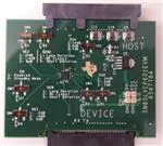
Figure 1. LVCP601 EVM
spacer
spacer
spacer
spacer
spacer
spacer
spacer
SLLU211 – October 2014
Submit Documentation Feedback
LVCP601 Evaluation Module
Copyright © 2014, Texas Instruments Incorporated
1
�www.ti.com
spacer
spacer
1
2
3
Contents
Introduction ...................................................................................................................
LVCP601 Evaluation Module Configuration ..............................................................................
PCB Construction ............................................................................................................
3.1
EVM Board Schematics ............................................................................................
3.2
EVM PCB Layout ...................................................................................................
3.3
LVCP601 EVM Bill of Materials ...................................................................................
3
3
5
5
6
8
List of Figures
2
1
LVCP601 EVM ............................................................................................................... 1
2
SN75LVCP601 EVM Schematic ........................................................................................... 5
3
PCB Layout of Top Layer ................................................................................................... 6
4
PCB Layout of 2nd Layer ................................................................................................... 6
5
PCB Layout of 3rd Layer
6
PCB Layout of Bottom Layer ............................................................................................... 7
...................................................................................................
LVCP601 Evaluation Module
7
SLLU211 – October 2014
Submit Documentation Feedback
Copyright © 2014, Texas Instruments Incorporated
�Introduction
www.ti.com
1
Introduction
The LVCP601 is a dual channel, single lane SATA redriver and signal conditioner. This guide describes
the construction and usage of the EVM for the LVCP601 which is meant to serve as an evaluation tool for
the LVCP601, as well as be used as a reference design for the device.
2
LVCP601 Evaluation Module Configuration
Kit Contents:
This EVM kit should contain the following items:
• LVCP601 EVM board
• This user’s manual
This board is designed to facilitate easy evaluation of the LVCP601 using internal SATA connectors.
Physical switches allow for simple configuration of the equalization, de-emphasis, and operation mode
settings of the LVCP601. The EVM board has two internal SATA connectors, one for the host side and
one for the device side of the redriver. This module also runs on a 3-V supply voltage that is derived from
the standard SATA power connection.
The configuration of the equalization, de-emphasis, de-emphasis width, and standby mode settings are all
selected using SW1-SW7. See Table 1 for further details about the configuration of the EVM. Suggested
default configuration settings for the EVM can be found in Table 2.
Table 1. Configuration of EVM Using Control Switches
Control Switch
Switch Position and
Corresponding Setting Configuration
SW1: EQ2 (Equalizer 2 configuration)
1: 14 dB
2: 0 dB
3: 7 dB
SW2: EQ1 (Equalizer 1 configuration)
1: 14 dB
2: 0 dB
3: 7 dB
SW3: DEW1 (De-emphasis width 1)
1: Long duration
2: Long duration
3: Short duration
SW4: DE1 (De-emphasis 1 configuration)
1: -2dB
2: -4 dB
3: 0 dB
SW5: DE2 (De-emphasis 2 configuration)
1: -2 dB
2: -4 dB
3: 0 dB
SW6: DEW2 (De-emphasis width 2)
1: Long duration
2: Long duration
3: Short duration
SW7: EN (Enable/Standby mode configuration)
1: Enabled
2: Standby Mode
3: Standby Mode
SLLU211 – October 2014
Submit Documentation Feedback
LVCP601 Evaluation Module
Copyright © 2014, Texas Instruments Incorporated
3
�LVCP601 Evaluation Module Configuration
www.ti.com
Table 2. Suggested Default Configuration for EVM
4
Parameter
Default Setting
EQ2
0 dB
EQ1
0 dB
DEW1
Long
DE1
0 dB
DE2
0 dB
DEW2
Long
EN
Enable Mode
LVCP601 Evaluation Module
SLLU211 – October 2014
Submit Documentation Feedback
Copyright © 2014, Texas Instruments Incorporated
�PCB Construction
www.ti.com
3
PCB Construction
This section contains the schematics, PCB layouts, and the bill of materials.
3.1
EVM Board Schematics
Figure 2 illustrates the SN75LVCP601 EVM schematic.
Figure 2. SN75LVCP601 EVM Schematic
SLLU211 – October 2014
Submit Documentation Feedback
LVCP601 Evaluation Module
Copyright © 2014, Texas Instruments Incorporated
5
�PCB Construction
3.2
www.ti.com
EVM PCB Layout
Figure 3 through Figure 6 illustrate the PCB layouts.
Figure 3. PCB Layout of Top Layer
Figure 4. PCB Layout of 2nd Layer
6
LVCP601 Evaluation Module
SLLU211 – October 2014
Submit Documentation Feedback
Copyright © 2014, Texas Instruments Incorporated
�PCB Construction
www.ti.com
Figure 5. PCB Layout of 3rd Layer
Figure 6. PCB Layout of Bottom Layer
3.2.1
EVM PCB Fabrication
The EVM board is a 4-layer board constructed of FR4-PolyClad 370 material. The board consists of a
signal layer on top, a ground layer, a power layer, and another signal layer on the bottom. The impedance
of the differential traces is 100 ohms. Other traces have an impedance of 50 ohms.
NOTE: In order to achieve the desired impedance, it is recommended that you consult your board
manufacturer for their process and design requirements.
SLLU211 – October 2014
Submit Documentation Feedback
LVCP601 Evaluation Module
Copyright © 2014, Texas Instruments Incorporated
7
�PCB Construction
3.3
www.ti.com
LVCP601 EVM Bill of Materials
Table 3 lists the SN75LVCP601 bill of materials.
Table 3. Bill of Materials
8
Item Qty
Reference
Value
1
1
CN1
SATA MALE 5622-6309-ML 3M5555-ND
Digikey P/N
5622-6309-ML
2
1
CN2
SATA Female
609-1029-ND
10031569-001LF
3
8
C1,C2,C3,C4,C5,C6,C7,C8
.012uF
490-3255-1-ND
GRM155R71C123KA01D
4
3
C9,C10,C11
47uf
587-1436-1-ND
EMK325BJ476MM-T
5
2
C12,C18
10uF
445-4112-1-ND
C1608X5R0J106M
6
2
C13,C14
1uf
PCC2422CT-ND
ECJ-1VB1E105K
7
4
C15,C16,C17,C19
0.1uF
445-4984-1-ND
C1005X5R1A104M
8
1
D1
LED Green 0805
67-1553-6-ND
SML-LXT0805GW-TR
9
2
J1,J2
HDR2X1 M .1
A26520-02-ND
4-103321-0-02
10
7
R1,R2,R3,R4,R5,R6,R7
4.7K
P4.7KJCT-ND
ERJ-2GEJ472X
11
1
R8
0 Ohm
P0.0GCT-ND
ERJ-3GEY0R00V
12
1
R9
330 ohm
P330GCT-ND
ERJ-3GEYJ331V
13
6
SW1,SW2,SW3,SW4,SW5,
SW6
Switch CJS-1201
563-1023-2-ND
CJS-1201B1
14
1
SW7
Switch CJS-1200
563-1022-1-ND
CJS-1200B1
15
1
U1
SN75LVCP601
296-27627-1-ND
SN75LVCP601RTJT
16
1
U2
REG104A-33
REG104GA-3.3-ND
REG104GA-3.3
LVCP601 Evaluation Module
Manufacturer P/N
SLLU211 – October 2014
Submit Documentation Feedback
Copyright © 2014, Texas Instruments Incorporated
�IMPORTANT NOTICE
Texas Instruments Incorporated and its subsidiaries (TI) reserve the right to make corrections, enhancements, improvements and other
changes to its semiconductor products and services per JESD46, latest issue, and to discontinue any product or service per JESD48, latest
issue. Buyers should obtain the latest relevant information before placing orders and should verify that such information is current and
complete. All semiconductor products (also referred to herein as “components”) are sold subject to TI’s terms and conditions of sale
supplied at the time of order acknowledgment.
TI warrants performance of its components to the specifications applicable at the time of sale, in accordance with the warranty in TI’s terms
and conditions of sale of semiconductor products. Testing and other quality control techniques are used to the extent TI deems necessary
to support this warranty. Except where mandated by applicable law, testing of all parameters of each component is not necessarily
performed.
TI assumes no liability for applications assistance or the design of Buyers’ products. Buyers are responsible for their products and
applications using TI components. To minimize the risks associated with Buyers’ products and applications, Buyers should provide
adequate design and operating safeguards.
TI does not warrant or represent that any license, either express or implied, is granted under any patent right, copyright, mask work right, or
other intellectual property right relating to any combination, machine, or process in which TI components or services are used. Information
published by TI regarding third-party products or services does not constitute a license to use such products or services or a warranty or
endorsement thereof. Use of such information may require a license from a third party under the patents or other intellectual property of the
third party, or a license from TI under the patents or other intellectual property of TI.
Reproduction of significant portions of TI information in TI data books or data sheets is permissible only if reproduction is without alteration
and is accompanied by all associated warranties, conditions, limitations, and notices. TI is not responsible or liable for such altered
documentation. Information of third parties may be subject to additional restrictions.
Resale of TI components or services with statements different from or beyond the parameters stated by TI for that component or service
voids all express and any implied warranties for the associated TI component or service and is an unfair and deceptive business practice.
TI is not responsible or liable for any such statements.
Buyer acknowledges and agrees that it is solely responsible for compliance with all legal, regulatory and safety-related requirements
concerning its products, and any use of TI components in its applications, notwithstanding any applications-related information or support
that may be provided by TI. Buyer represents and agrees that it has all the necessary expertise to create and implement safeguards which
anticipate dangerous consequences of failures, monitor failures and their consequences, lessen the likelihood of failures that might cause
harm and take appropriate remedial actions. Buyer will fully indemnify TI and its representatives against any damages arising out of the use
of any TI components in safety-critical applications.
In some cases, TI components may be promoted specifically to facilitate safety-related applications. With such components, TI’s goal is to
help enable customers to design and create their own end-product solutions that meet applicable functional safety standards and
requirements. Nonetheless, such components are subject to these terms.
No TI components are authorized for use in FDA Class III (or similar life-critical medical equipment) unless authorized officers of the parties
have executed a special agreement specifically governing such use.
Only those TI components which TI has specifically designated as military grade or “enhanced plastic” are designed and intended for use in
military/aerospace applications or environments. Buyer acknowledges and agrees that any military or aerospace use of TI components
which have not been so designated is solely at the Buyer's risk, and that Buyer is solely responsible for compliance with all legal and
regulatory requirements in connection with such use.
TI has specifically designated certain components as meeting ISO/TS16949 requirements, mainly for automotive use. In any case of use of
non-designated products, TI will not be responsible for any failure to meet ISO/TS16949.
Products
Applications
Audio
www.ti.com/audio
Automotive and Transportation
www.ti.com/automotive
Amplifiers
amplifier.ti.com
Communications and Telecom
www.ti.com/communications
Data Converters
dataconverter.ti.com
Computers and Peripherals
www.ti.com/computers
DLP® Products
www.dlp.com
Consumer Electronics
www.ti.com/consumer-apps
DSP
dsp.ti.com
Energy and Lighting
www.ti.com/energy
Clocks and Timers
www.ti.com/clocks
Industrial
www.ti.com/industrial
Interface
interface.ti.com
Medical
www.ti.com/medical
Logic
logic.ti.com
Security
www.ti.com/security
Power Mgmt
power.ti.com
Space, Avionics and Defense
www.ti.com/space-avionics-defense
Microcontrollers
microcontroller.ti.com
Video and Imaging
www.ti.com/video
RFID
www.ti-rfid.com
OMAP Applications Processors
www.ti.com/omap
TI E2E Community
e2e.ti.com
Wireless Connectivity
www.ti.com/wirelessconnectivity
Mailing Address: Texas Instruments, Post Office Box 655303, Dallas, Texas 75265
Copyright © 2014, Texas Instruments Incorporated
�