SN75LVDM976
SN75LVDM977
www.ti.com
SLLS292B – APRIL 1998 – REVISED JANUARY 2000
9-CHANNEL DUAL-MODE TRANSCEIVERS
FEATURES
•
•
•
•
•
•
•
•
•
•
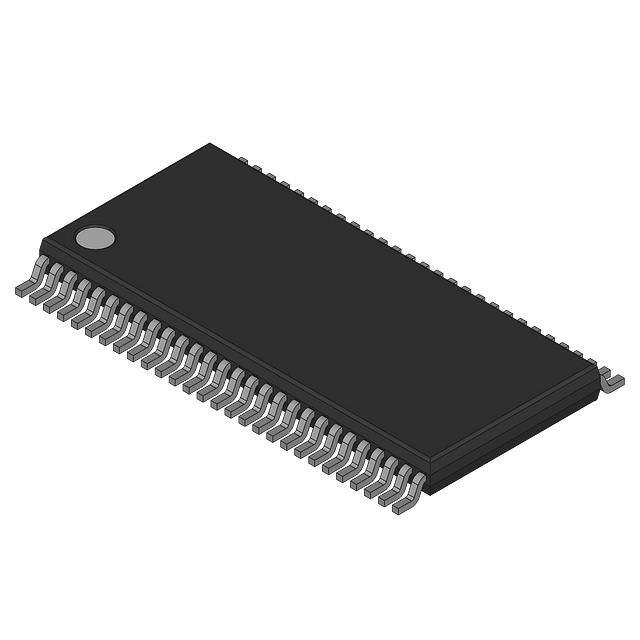
DGG PACKAGE
(TOP VIEW)
9 Channels for the Data and Control Paths of
the Small Computer Systems Interface (SCSI)
Supports Single-Ended and Low-Voltage
Differential (LVD) SCSI
CMOS Input Levels ('LVDM976) or TTL Input
Levels ('LVDM977) Available
Includes DIFFSENS Comparators on CDE0
Single-Ended Receivers Include Noise Pulse
Rejection Circuitry
Packaged in Thin Shrink Small-Outline
Package With 20-Mil Terminal Pitch
Low Disabled Supply Current 7 mA Maximum
Power-Up/Down Glitch Protection
Bus is High-Impedance With VCC = 1.5 V
Pin-Compatible With the SN75976ADGG
High-Voltage Differential Transceiver
INV/NON
GND
GND
1A
1DE/RE
2A
2DE/RE
3A
3DE/RE
4A
4DE/RE
VCC
GND
GND
GND
GND
GND
VCC
5A
5DE/RE
6A
6DE/RE
7A
7DE/RE
8A
8DE/RE
9A
9DE/RE
DESCRIPTION
The SN75LVDM976 and SN75LVDM977 have nine
transceivers for transmitting or receiving the signals
to or from a SCSI data bus. They offer electrical
compatibility to both the single-ended signaling of
X3.277:1996-SCSI-3 Parallel Interface (Fast-20) and
the new low-voltage differential signaling method of
proposed standard 1142-D SCSI Parallel Interface –
2 (SPI-2).
The differential drivers are nonsymmetrical. The SCSI
bus uses a dc bias on the line to allow terminated fail
safe and wired-OR signaling. This bias can be as
high as 125 mV and induces a difference in the
high-to-low and low-to-high transition times of a
symmetrical driver. In order to reduce pulse skew, an
LVD SCSI driver's output characteristics become
nonsymmetrical. In other words, there is more
assertion current than negation current to or from the
driver. This allows the actual differential signal
voltage on the bus to be symmetrical about 0 V. Even
though the driver output characteristics are
nonsymmetrical, the design of the 'LVDM976 drivers
maintains balanced signaling. Balanced means that
the current that flows in each signal line is nearly
equal but opposite in direction and is one of the keys
to the low-noise performance of a differential bus.
1
56
2
55
3
54
4
53
5
52
6
51
7
50
8
49
9
48
10
47
11
46
12
45
13
44
14
43
15
42
16
41
17
40
18
39
19
38
20
37
21
36
22
35
23
34
24
33
25
32
26
31
27
30
28
29
CDE2
CDE1
CDE0
9B+
9B–
8B+
8B–
7B+
7B–
6B+
6B–
VCC
GND
GND
GND
GND
GND
VCC
5B+
5B–
4B+
4B–
3B+
3B–
2B+
2B–
1B+
1B–
AVAILABLE OPTIONS
PACKAGE
(1)
TA
TSSOP (DGG)
CMOS INPUT LEVELS
TSSOP (DGG)
TTL INPUTS
LEVELS
0°C to
70°C
SN75LVDM976DGG
SN75LVDM976DGGR (1)
SN75LVDM977DGG
SN75LVDM977DGGR (1)
The R suffix designates a taped and reeled package.
Please be aware that an important notice concerning availability, standard warranty, and use in critical applications of Texas
Instruments semiconductor products and disclaimers thereto appears at the end of this data sheet.
PRODUCTION DATA information is current as of publication date.
Products conform to specifications per the terms of the Texas
Instruments standard warranty. Production processing does not
necessarily include testing of all parameters.
Copyright © 1998–2000, Texas Instruments Incorporated
�SN75LVDM976
SN75LVDM977
www.ti.com
SLLS292B – APRIL 1998 – REVISED JANUARY 2000
DESCRIPTION (CONTINUED)
The signal symmetry requirements of the LVD-SCSI bus mean you can no longer obtain logical inversion of a
signal by simply reversing the differential signal connections. This requires the ability to invert the logic
convention through the INV/NON terminal. This input would be a low for SCSI controllers with active-high data
and high for active-low data. In either case, the B+ signals of the transceiver must be connected to the SIGNAL+
line of the SCSI bus and the B- of the transceiver to the SIGNAL- line.
The CDE0 input incorporates a window comparator to detect the status of the DIFFSENS line of a SCSI bus.
This line is below 0.5 V, if using single-ended signals, between 1.7 V and 1.9 V if low-voltage differential, and
between 2.4 V and 5.5 V if high-voltage differential. The outputs assume the characteristics of single-ended or
LVD accordingly or place the outputs into high-impedance, when HVD is detected. This, and the INV/NON input,
are the only differences to the trade-standard function of the SN75976A HVD transceiver.
Two options are offered to minimize the signal noise margins on the interface between the communications
controller and the transceiver. The SN75LVDM976 has logic input voltage thresholds of about 0.5 VCC. The
SN75LVDM977 has a fixed logic input voltage threshold of about 1.5 V. The input voltage threshold should be
selected to be near the middle of the output voltage swing of the corresponding driver circuit.
The SN75LVDM976 and SN75LVDM977 are characterized for operation over an free-air temperature range of TA
= 0°C to 70°C.
2
Submit Documentation Feedback
�SN75LVDM976
SN75LVDM977
www.ti.com
SLLS292B – APRIL 1998 – REVISED JANUARY 2000
LOGIC DIAGRAM (POSITIVE LOGIC)
CDE1
+
–
LVD
B
SE
INV/NON
–
+
A
2.4 V
(Internal)
CDE0
0.5 V
(Internal)
1DEb
1DE/RE
1REb
1DEb
1DEa
1A
1B–
1DEa
1B+
1REa
1REb
1REa
2A
2DE/RE
3A
3DE/RE
4A
4DE/RE
2B–
2B+
3B–
3B+
4B–
4B+
Channel 2
Channel 3
Channel 4
INV/NON
SE
LVD
CDE2
5A
5DE/RE
6A
6DE/RE
7A
7DE/RE
8A
8DE/RE
5B–
5B+
6B–
6B+
7B–
7B+
8B–
8B+
Channel 5
Channel 6
Channel 7
Channel 8
INV/NON
SE
9DEb
9DE/RE
9A
LVD
9DEb
9DEa
9REb
9B–
9DEa
9B+
9REa
9REb
9REa
Submit Documentation Feedback
3
�SN75LVDM976
SN75LVDM977
www.ti.com
SLLS292B – APRIL 1998 – REVISED JANUARY 2000
LOGIC DIAGRAMS AND FUNCTION TABLES
A
FUNCTION TABLE
B−
VID
B+
DE/RE
Figure 1. Inverting LVD Transceiver
A
INPUTS
OUTPUTS
(B+ – B–)
DE/RE
A
B+
B–
A
VID ≥ 30 mV
L
NA
Z
Z
L
–30 mV < VID < 30
mV
L
NA
Z
Z
?
VID– 30 mV
L
NA
Z
Z
H
Open circuit
L
NA
Z
Z
?
NA
H
L
H
L
Z
NA
H
H
L
H
Z
B−
FUNCTION TABLE
DE/RE
INPUTS
B+
Figure 2. Inverting Single-Ended Transceiver
A
OUTPUTS
B–
DE/RE
A
B+
B–
H
L
NA
L
Z
A
L
L
L
NA
L
Z
H
Open circuit
L
NA
L
Z
?
NA
H
L
L
H
Z
NA
H
H
L
L
Z
FUNCTION TABLE
B−
INPUT
B+
OUTPUTS
A
B+
B–
L
L
H
H
L
L
Figure 3. Inverting Single-Ended Driver
FUNCTION TABLE
B−
A
B+
Figure 4. Inverting LVD Driver
4
INPUT
OUTPUTS
A
B+
B–
L
H
L
H
L
H
Submit Documentation Feedback
�SN75LVDM976
SN75LVDM977
www.ti.com
SLLS292B – APRIL 1998 – REVISED JANUARY 2000
FUNCTION TABLE
B−
INPUT
B+
A
B+
B–
L
L
H
H
H
L
A
Figure 5. Noninverting LVD Driver
A
FUNCTION TABLE
B−
VID
INPUTS
B+
DE/RE
Figure 6. Noninverting LVD Transceiver
A
OUTPUTS
OUTPUTS
(B+ – B–)
DE/RE
A
B+
B–
A
VID ≥ 30 mV
L
NA
Z
Z
H
–30 mV < VID < 30
mV
L
NA
Z
Z
?
VID≤– 30 mV
L
NA
Z
Z
L
Open circuit
L
NA
Z
Z
?
NA
H
L
L
H
Z
NA
H
H
H
L
Z
B−
FUNCTION TABLE
DE/RE
INPUTS
B+
Figure 7. Noninverting Single-Ended Transceiver
A
OUTPUTS
B–
DE/RE
A
B+
B–
A
H
L
NA
L
Z
H
L
L
NA
L
Z
L
Open circuit
L
NA
L
Z
?
NA
H
L
L
L
Z
NA
H
H
L
H
Z
B−
FUNCTION TABLE
INPUT
B+
OUTPUTS
A
B+
B–
L
L
L
H
L
H
Figure 8. Noninverting Single-Ended Driver
Submit Documentation Feedback
5
�SN75LVDM976
SN75LVDM977
www.ti.com
SLLS292B – APRIL 1998 – REVISED JANUARY 2000
1B−
1A
1B+
1DE/RE
2B−
2A
2B+
2DE/RE
3B−
3A
3B+
3DE/RE
4B−
4A
4B+
4DE/RE
5B−
5A
1B−
1A
1B+
1DE/RE
2B+
2DE/RE
3B−
3A
6B+
6DE/RE
7B−
7A
8B−
8A
8B+
8DE/RE
9B−
9A
9B+
9DE/RE
Control Inputs
CDE0
0.7 V < VI < 1.9 V
INV/NON
L
CDE1
L
CDE2
L
(a)
4B+
4DE/RE
5B−
5A
5B+
3B−
3A
3B+
4B−
4A
4B+
5B−
5A
5B+
5DE/RE
6B−
6A
6B+
7B−
7A
7B+
6B−
6A
6B+
6DE/RE
7B−
7A
7B+
7DE/RE
8B−
8A
8B+
9B−
9A
9B+
9DE/RE
8B−
8A
8B+
8DE/RE
9B−
9A
9B+
9DE/RE
Control Inputs
CDE0
0.7 V < VI < 1.9 V
INV/NON
L
CDE1
L
CDE2
H
Control Inputs
CDE0
0.7 V < VI < 1.9 V
INV/NON
L
CDE1
H
CDE2
L
(b)
(c)
Figure 9. Logic Diagrams
6
2B+
4B−
4A
7B+
7DE/RE
2B−
2A
3B+
3DE/RE
6B−
6A
1B+
2B−
2A
5B+
5DE/RE
1B−
1A
Submit Documentation Feedback
�SN75LVDM976
SN75LVDM977
www.ti.com
SLLS292B – APRIL 1998 – REVISED JANUARY 2000
1B−
1A
1B+
2A
1B−
1A
1B+
1DE/RE
2B−
2A
2B+
2DE/RE
3B−
3A
3B+
3DE/RE
4B−
4A
4B+
4DE/RE
5B−
5A
5B+
5DE/RE
1B−
1A
1B+
1DE/RE
2B−
2B+
2B−
2A
2B+
2DE/RE
3B−
3A
4A
5A
6B−
6A
6B+
7A
8A
3B+
4B−
4B+
7B+
7DE/RE
8B−
8A
8B+
8DE/RE
9B+
9DE/RE
5B+
(a)
5B−
5A
5B+
6B−
6B+
6B−
6A
6B+
7B−
7B+
7B−
7A
7B+
8B−
8B+
8B−
8A
8B+
9B−
9A
9B+
9DE/RE
Control Inputs
CDE0
0.7 V < VI < 1.9 V
L
INV/NON
CDE1
H
CDE2
H
4B+
5B−
9B−
9A
4B−
4A
4DE/RE
6DE/RE
7A
3B+
3DE/RE
6A
7B−
3B−
3A
9B−
9A
9B+
9DE/RE
Control Inputs
CDE0
0.7 V < VI < 1.9 V
H
INV/NON
CDE1
L
CDE2
L
(b)
Control Inputs
CDE0
0.7 V < VI < 1.9 V
INV/NON
H
CDE1
L
CDE2
H
(C)
Figure 10. Logic Diagrams
Submit Documentation Feedback
7
�SN75LVDM976
SN75LVDM977
www.ti.com
SLLS292B – APRIL 1998 – REVISED JANUARY 2000
1B−
1A
1B+
1A
1B−
1DE/RE
1A
1B−
1DE/RE
1B+
2B−
2A
2B+
2A
2B−
2DE/RE
1B+
2A
2B−
2DE/RE
2B+
3B−
3A
3B+
3B−
3A
3DE/RE
2B+
3B−
3A
3DE/RE
3B+
4B−
4A
4B+
4B−
4A
4DE/RE
3B+
4B−
4A
4DE/RE
4B+
5B−
5A
5B+
5A
5B−
4B+
5A
5B−
5DE/RE
5B+
5B+
6B−
6A
6B+
6A
6B−
6A
6B−
6DE/RE
6B+
6B+
7B−
7A
7B+
7A
7B−
7A
7B−
7DE/RE
7B+
7B+
8B−
8A
8B+
8A
8B−
8A
8B−
8DE/RE
8B+
8B+
9B−
9A
9B+
9DE/RE
9A
9B−
9DE/RE
9A
9B−
9DE/RE
9B+
Control Inputs
CDE0
0.7 V < VI < 1.9 V
INV/NON
H
CDE1
H
CDE2
H
(a)
Control Inputs
CDE0
VI < 0.5 V
INV/NON
L
CDE1
L
CDE2
L
(b)
Figure 11. Logic Diagrams
8
Submit Documentation Feedback
9B+
Control Inputs
CDE0
VI < 0.5 V
INV/NON
L
CDE1
L
CDE2
H
(c)
�SN75LVDM976
SN75LVDM977
www.ti.com
SLLS292B – APRIL 1998 – REVISED JANUARY 2000
1A
1B−
1A
1A
1B−
1B−
1DE/RE
1B+
1B+
1B+
2A
2B−
2A
2A
2B−
2B−
2DE/RE
2B+
2B+
2B+
3A
3B−
3B−
3A
3B−
3A
3DE/RE
3B+
3B+
3B+
4A
4B−
4A
4B−
4A
4B−
4DE/RE
4B+
4B+
4B+
5A
5B−
5A
5A
5B−
5DE/RE
5B−
5DE/RE
5B+
5B+
6A
6B−
5B+
6A
6B−
6A
6B−
6DE/RE
6DE/RE
6B+
6B+
7A
7B−
7DE/RE
6B+
7A
7B−
7A
7B−
7DE/RE
7B+
7B+
8A
8B−
8DE/RE
7B+
8A
8B−
8A
8B−
8DE/RE
8B+
8B+
9A
9B−
9DE/RE
8B+
9A
9B−
9DE/RE
9B+
Control Inputs
CDE0
VI < 0.5 V
INV/NON
L
CDE1
H
CDE2
L
(a)
9B−
9A
9DE/RE
9B+
9B+
Control Inputs
CDE0
VI < 0.5 V
INV/NON
L
CDE1
H
CDE2
H
(b)
Control Inputs
CDE0
VI < 0.5 V
INV/NON
H
CDE1
L
CDE2
L
(c)
Figure 12. Logic Diagrams
Submit Documentation Feedback
9
�SN75LVDM976
SN75LVDM977
www.ti.com
SLLS292B – APRIL 1998 – REVISED JANUARY 2000
1A
1B−
1B−
1A
1B−
1A
1DE/RE
1B+
1B+
1B+
2A
2B−
2B−
2A
2A
2B−
2DE/RE
2B+
2B+
2B+
3A
3B−
3B−
3A
3B−
3A
3DE/RE
3B+
3B+
3B+
4A
4B−
4B−
4A
4B−
4A
4DE/RE
4B+
4B+
4B+
5A
5B−
5B−
5A
5B−
5A
5DE/RE
5B+
5B+
5B+
6A
6B−
6B−
6A
6B−
6A
6DE/RE
6B+
6B+
6B+
7A
7B−
7B−
7A
7B−
7A
7DE/RE
7B+
7B+
7B+
8A
8B−
8B−
8A
8B−
8A
8DE/RE
8B+
8B+
8B+
9A
9B−
9B−
9A
9DE/RE
9DE/RE
9DE/RE
9B+
9B+
Control Inputs
CDE0
VI < 0.5 V
INV/NON
H
CDE1
L
CDE2
H
(a)
Control Inputs
CDE0
VI < 0.5 V
INV/NON
H
CDE1
H
CDE2
L
(b)
Figure 13. Logic Diagrams
10
9B−
9A
Submit Documentation Feedback
9B+
Control Inputs
CDE0
VI < 0.5 V
H
INV/NON
CDE1
H
CDE2
H
(c)
�SN75LVDM976
SN75LVDM977
www.ti.com
SLLS292B – APRIL 1998 – REVISED JANUARY 2000
1A
High Z
1B–
1B+
High Z
High Z
2A
High Z
2B–
2B+
High Z
High Z
3B–
3B+
3A
High Z
High Z
High Z
4B–
4B+
4A
High Z
High Z
High Z
5A
High Z
5B–
5B+
High Z
High Z
6A
High Z
6B–
6B+
High Z
High Z
7A
High Z
7B–
7B+
High Z
High Z
8A
High Z
8B–
8B+
High Z
High Z
9A
High Z
9B–
9B+
High Z
High Z
Control Inputs
CDE0
VI > 2.5 V
INV/NON
X
CDE1
X
CDE2
X
Figure 14. Logic Diagrams
Submit Documentation Feedback
11
�SN75LVDM976
SN75LVDM977
www.ti.com
SLLS292B – APRIL 1998 – REVISED JANUARY 2000
INPUT AND OUTPUT EQUIVALENT SCHEMATIC DIAGRAMS
CDE1, CDE2, DE/RE Inputs
A and INV/NON Inputs
VCC
VCC
10uA
Input
Input
10uA
CDE0 Input
A Output
VCC
VCC
Input
A
B+ Input
B– Input
Iref
Iref
37 Ω
37 Ω
BP
Iref
BN
Iref
113 Ω
113 Ω
VCC
15 Ω
12
VCC
VCC
15 Ω
15 Ω
Submit Documentation Feedback
113 Ω
�SN75LVDM976
SN75LVDM977
www.ti.com
SLLS292B – APRIL 1998 – REVISED JANUARY 2000
Terminal Functions
TERMINAL
NAME
NO.
'LVDM976
Logic
Level
'LVDM977
Logic
Level
I/O
Terminat
ion
DESCRIPTION
1A - 9A
4,6,8,10,
19,21,23,
25,27
CMOS
TTL
I/O
Pullup
1A - 9A carry data to and from the communication controller.
1B–– 9B–
29,31,33,
35,37,46,
48,50,52
LVD or
TTL
LVD or
TTL
I/O
None
1B- to 9B- are the signals to and from the data bus. When INV/NON
is low, the logic sense is the opposite that of the A input (inverted).
When INV/NON is high, the logic sense is the same as the A input
(noninverted).
1B+ - 9B+
30,32,34,
36,38,47,
49,51,53
LVD or
GND
LVD or
GND
I/O
None
When in the LVD mode, 1B+ - 9B+ are signals to or from the data
bus and follow the same logic sense as the A input when INV/NON
is low (noninverted). The logic sense is opposite that of the A input
(inverted) when INV/NON is high. When in single-ended mode,
these terminals become a ground connection through a transistor
and do not switch.
CDE0
54
Trinary
Trinary
Input
None
CDE0 is the common driver enable 0. With the driver enabled and
the CDE0 input less than 0.5 V, the driver output is single-ended
mode. With the driver enabled and the CDE0 input between 0.7 V
and 1.9 V the driver output is LVD mode. All drivers are disabled
when the input is greater than 2.4 V.
CDE1
55
CMOS
TTL
Input
Pulldown CDE1 is the common driver enable 1. When CDE1 is high, drivers
1–4 are enabled
CDE2
56
CMOS
TTL
Input
Pulldown CDE2 is the common driver enable 2. When CDE2 is high, drivers 5
to 8 are enabled.
1DE/RE 9DE/RE
5,7,9,11,
20,22,24,
26,28
CMOS
TTL
Input
Pulldown 1DE/RE–9DE/RE are direction controls that transmit data to the bus
when it is high and CDE0 is below 2.2 V. Data is received from the
bus when 1DE/RE- 9DE/RE, CDE1, and CDE2 are low.
GND
2,3,13,14,
15,16,17,
40,41,42,
43,44
NA
NA
Power
NA
INV/NON
1
CMOS
CMOS
Input
Pullup
VCC
12,18,39,
45
NA
NA
Power
NA
GND is the circuit ground.
A high-level input to INV/NON inverts the logic to and from the A
terminals. (i.e., the voltage at A terminal and the corresponding Bterminal are in phase.)
Supply voltage
ABSOLUTE MAXIMUM RATINGS
over operating free-air temperature range (unless otherwise noted) (1)
UNIT
VCC
Supply voltage range (2)
VI
Input voltage range
–0.5 V to 7 V
(A, INV/NON)
(DE/RE, B+, B-, CDE0, CDE1, CDE2)
Continuous total power dissipation
Tstg
(2)
–0.5 V to 5.25 V
See Dissipation Rating Table
Storage temperature range,
–65°C to 150°C
Lead temperature 1,6 mm (1/16 inch) from case for 10 seconds
(1)
–0.5 V to VCC + 0.5 V
260°C
Stresses beyond those listed under absolute maximum ratings may cause permanent damage to the device. These are stress ratings
only, and functional operation of the device at these or any other conditions beyond those indicated under recommended operating
conditions is not implied. Exposure to absolute-maximum-rated conditions for extended periods may affect device reliability.
All voltage values are with respect to GND unless otherwise noted.
Submit Documentation Feedback
13
�SN75LVDM976
SN75LVDM977
www.ti.com
SLLS292B – APRIL 1998 – REVISED JANUARY 2000
DISSIPATION RATING TABLE
PACKAGE
TA≤ 25°C
POWER RATING
DERATING FACTOR
ABOVE TA = 25°C
TA = 70°C
POWER RATING
DGG
978 mW
10.8 mW/°C
492 mW
RECOMMENDED OPERATING CONDITIONS (see Figure 15)
VCC
Supply voltage
VIH
High-level input voltage
VIL
Low-level input voltage
|VID|
Differential input voltage
VIC
Common-mode input voltage
VOD(bias)
Differential output voltage
bias
IOH
High-level output current
IOL
Low-level output current
ZL
Differential load impedance
TA
Operating free-air temperature
MIN
NOM
MAX
UNIT
4.75
5
5.25
V
SN75LVDM976
0.7 VCC
SN75LVDM977
2
V
SN75LVDM976
0.3 VCC
SN75LVDM977
0.8
Differential receiver
Differential
V
0.03
3.6
V
0.7
1.8
V
100
125
mV
Single-ended driver
7
Receiver
2
Single-ended driver
48
Receiver
2
mA
mA
40
65
Ω
0
70
°C
ELECTRICAL CHARACTERISTICS
over recommended operating free-air temperature range (unless otherwise noted)
PARAMETER
IIH
High-level input current
IIL
Low-level input current
MIN TYP (1)
TEST CONDITIONS
CDE1 and CDE2
50
INV/NON
50
CDE1 and CDE2
50
INV/NON
50
Disabled
ICC
CI
Supply current
Input capacitance
No load
26
Single-ended drivers enabled,
No load
10
LVD receivers enabled,
No load
26
Singled-ended receivers enabled,
No load
VI = 0.2 sin (2 π (1E06)t) + 0.5 ± 0.01 V
Bus terminal
14
All typical values are at VCC = 5 V, TA = 25°C.
Submit Documentation Feedback
UNIT
µA
µA
7
LVD drivers enabled,
∆CI Difference in input capacitance between B+ and B–
(1)
MAX
mA
7
9.5
0.2
pF
�SN75LVDM976
SN75LVDM977
www.ti.com
SLLS292B – APRIL 1998 – REVISED JANUARY 2000
DIFFSENS (CDE0) RECEIVER ELECTRICAL CHARACTERISTICS
over recommended operating free-air temperature range (unless otherwise noted)
PARAMETER
TEST CONDITIONS
MIN
TYP (
1)
MAX
UNIT
VIT1
Input threshold voltage
0.5
0.6
0.7
VIT2
Input threshold voltage
1.9
2.1
2.4
II
Input current
0 V ≤ VI ≤ 2.7 V
±1
µA
II(OFF)
Power-off input current
VCC = 0, 0 V ≤ VI ≤ 2.7 V
±1
µA
(1)
V
All typical values are at VCC = 5 V, TA = 25°C.
LVD DRIVER ELECTRICAL CHARACTERISTICS
over recommended operating free-air temperature range (unless otherwise noted)
PARAMETER
TEST CONDITIONS
Driver differential high-level output
voltage
VOD(H)
Driver differential low-level output
voltage
VOD(L)
VI(1) = 0.96 V, VI(2) = 0.53 V,
See Figure 16
MIN
TYP (1)
270
460
MAX
780
0.69|VOD(L) |+50
270
VI(1) = 1.96 V, VI(2) = 1.53 V,
See Figure 16
UNIT
1.45|VOD(L) |–65
500
780
0.69|VOD(L) |+50
mV
1.45|VOD(L) |–65
VI(1) = 0.96 V, VI(2) = 0.53 V,
See Figure 16
260
400
640
VI(1) = 1.96 V, VI(2) = 1.53 V,
See Figure 16
260
400
640
1.1
1.2
1.5
V
±50
±120
mV
80
150
mV
mV
VOC(SS)
Steady-state common-mode output
voltage
∆VOC(SS)
Change in steady-state
common-mode output voltage
between logic states
VOC(PP)
Peak-to-peak common-mode
output voltage
IIH
High-level input current
IIL
Low-level input current
IO(OFF)
Power-off output current
VCC = 0, 0 V ≤ VO ≤ 2.5 V
±1
µA
IOS
Short-circuit output current
0 V ≤ VO ≤ 2.5 V
±24
mA
IOZ
High-impedance output current
VO = 0 or 2.5 V
±1
µA
(1)
A
DE/RE
A
DE/RE
VI(1) = 1.41 V, VI(2) = 0.99 V,
See Figure 17
VIH = 3.3 V ('976) VIH = 2 V ('977)
VIL = 1.6 V ('976)VIL = 0.8 V ('977)
7
µA
50
30
µA
8
All typical values are at VCC = 5 V, TA = 25°C.
LVD DRIVER SWITCHING CHARACTERISTICS
over recommended operating conditions (unless otherwise noted) (See Figure 16)
PARAMETER
TEST CONDITIONS
tPLH
Propagation delay time, low-to-high level output
tPHL
Propagation delay time, high-to-low level output
tr
Differential output signal rise time
tf
Differential output signal fall time
tsk(p)
tsk(lim)
MIN
TYP (
1)
2.9
UNIT
8.8
ns
8.8
ns
1
3
6
ns
1
3
6
ns
Pulse skew (|tPHL– tPLH|)
3.7
ns
Skew limit (2)
5.9
ns
tPHZ
Propagation delay time, high-level to high-impedance output
50
ns
ten
Enable time, receiver to driver
33
ns
(1)
(2)
2.9
MAX
VCC = 5 V,
VI2 = 0.99 V,
VI1 = 1.41 V,
See Figure 18
VI1 = 1.41 V,
TA = 25°C
VI2 = 0.99 V,
All typical values are at VCC = 5 V, TA = 25°C.
tsk(lim) is the maximum delay time difference between any two drivers on any two devices operating at the same supply voltage and the
same ambient temperature.
Submit Documentation Feedback
15
�SN75LVDM976
SN75LVDM977
www.ti.com
SLLS292B – APRIL 1998 – REVISED JANUARY 2000
SINGLE-ENDED DRIVER ELECTRICAL CHARACTERISTICS
over recommended operating conditions (unless otherwise noted)
PARAMETER
VOH
High-level output voltage
VOL
Low-level output voltage
TEST CONDITIONS
IOH = –7 mA,
B– output
High-level input current
IIL
Low-level input current
IO(OFF)
Power-off output current
IOZ
High-impedance output current
MIN
2
IOH = 0 mA
B– output
IIH
See Figure 19
VCC = 5 V,
B+
A
IOL = 48 mA
A
B–
UNIT
3.24
V
3.7
V
0.5
V
–0.5
IOL = 25 mA
0.5
VIL = 1.6 V ('976), VIL = 0.8 V ('977)
DE/RE
MAX
IOL = –25 mA
VIH = 3.3 V ('976), VIH = 2 V ('977)
DE/RE
TYP
–7
50
–30
8
0 V ≤ VO ≤ 5.25 V
VCC = 0,
VO = 0 or VCC
V
µA
µA
±1
µA
±1
µA
SINGLE-ENDED DRIVER SWITCHING CHARACTERISTICS
over recommended operating conditions (unless otherwise noted)
PARAMETER
TEST CONDITIONS
MI TYP (
1) MAX
N
UNIT
tPLH
Propagation delay time, low-to-high level output
2.7
8.2
ns
tPHL
Propagation delay time, high-to-low level output
2.7
8.2
ns
tr
Differential output signal rise time
0.5
4
ns
tf
Differential output signal fall time
0.5
4
ns
tsk(p)
Pulse skew (|tPHL– tPLH|)
3.4
ns
tsk(lim)
Skew limit (2)
5.5
ns
ten
Enable time, receiver to driver
50
ns
30
ns
Propagation delay time, low-level to high-impedance
output
tPLZ
(1)
(2)
VCC = 5 V, TA = 25°C, See Figure 19
See Figure 20
All typical values are at VCC = 5 V, TA = 25°C.
tsk(lim) is the maximum delay time difference between any two drivers on any two devices operating at the same supply voltage and the
same ambient temperature.
LVD RECEIVER ELECTRICAL CHARACTERISTICS
over recommended operating conditions (unless otherwise noted)
PARAMETER
TEST CONDITIONS
MIN
TYP MAX
UNIT
VIT+
Positive-going differential input voltage threshold
VIT-
Negative-going differential input voltage threshold
VOH
High-level output voltage
IOH = –2 mA
VOL
Low-level output voltage
IOL = 2 mA
0.5
V
II
Input current, B+ or B–
VI = 0 V to 2.5 V
±1
µA
II(OFF
Power-off Input current, B+ or B–
VCC = 0,
±1
µA
IIH
High-level input current, DE/RE
VIH = 3.3 V ('976), VIH = 2 V ('977)
50
µA
IIL
Low-level input current, DE/RE
VIL = 1.6 V ('976), VIL = 0.8 V ('977)
IOZ
High-impedance output current
VO = 0 or VCC
)
16
See Figure 21
Submit Documentation Feedback
30
mV
–30
mV
3.7
VI = 0 V to 2.5 V
V
8
µA
±30
µA
�SN75LVDM976
SN75LVDM977
www.ti.com
SLLS292B – APRIL 1998 – REVISED JANUARY 2000
LVD RECEIVER SWITCHING CHARACTERISTICS
over recommended operating conditions (unless otherwise noted)
PARAMETER
TEST CONDITIONS
MIN
TYP (
1)
MAX
UNIT
tPLH
Propagation delay time, low-to-high level output
tPHL
Propagation delay time, high-to-low level output
tsk(p)
Pulse skew (|tPHL– tPLH|)
tr
Output signal rise time
tf
Output signal fall time
tsk(lim)
Skew limit (2)
tPHZ
Propagation delay time, high-level to high-impedance output
42
ns
tPLZ
Propagation delay time, low-level to high-impedance output
20
ns
ten
Enable time, driver to receiver
26
ns
(1)
(2)
4.5
10
ns
4.5
10
ns
3
ns
8
ns
8
ns
5.5
ns
VCC = 5 V, TA = 25°C, See
Figure 21
See Figure 18
All typical values are at VCC = 5 V, TA = 25°C.
tsk(lim) is the maximum delay time difference between any two drivers on any two devices operating at the same supply voltage and the
same ambient temperature.
SINGLE-ENDED RECEIVER ELECTRICAL CHARACTERISTICS
over recommended operating conditions (unless otherwise noted)
PARAMETER
TEST CONDITIONS
VIT+
Positive-going input voltage threshold B–
VIT–
Negative-going input voltage
threshold
VOH
High-level output voltage
IOH = –2 mA
VOL
Low-level output voltage
IOL = 2 mA
II
Input current
B–
II(OFF
Power-off Input current
IIH
IIL
IOZ
High-impedance output current
B–
MIN
TYP
MAX
1.6
1.9
1
1.1
3.7
4.6
V
V
V
0.5
V
VI = 0 to VCC
±1
µA
B–
VCC = 0 V, VI = 0 to 5.25 V
±1
µA
High-level input current
DE/RE
VIH = 3.3 V ('976), VIH = 2 V ('977)
50
µA
Low-level input current
DE/RE
VIL = 1.6 V ('976), VIL = 0.8 V ('977)
)
0.3
UNIT
8
µA
VO = 0 or VCC
-30
µA
SINGLE-ENDED RECEIVER SWITCHING CHARACTERISTICS
over recommended operating conditions (unless otherwise noted)
PARAMETER
TEST CONDITIONS
MIN
MAX
UNIT
7
TYP
12.5
ns
7
12.5
ns
3.5
ns
8
ns
8
ns
5.5
ns
tPLH
Propagation delay time, low-to-high level output
tPHL
Propagation delay time, high-to-low level output
tsk(p)
Pulse skew (|tPHL– tPLH|)
tr
Output signal rise time
tf
Output signal fall time
tsk(lim)
Skew limit (1)
tPHZ
Propagation delay time, high-level to high-impedance
output
20
ns
tPLZ
Propagation delay time, low-level to high-impedance
output
30
ns
ten
Enable time, driver to receiver
48
ns
(1)
VCC = 5 V, TA = 25°C, See
Figure 22
See Figure 20
tsk(lim) is the maximum delay time difference between any two drivers on any two devices operating at the same supply voltage and the
same ambient temperature.
Submit Documentation Feedback
17
�SN75LVDM976
SN75LVDM977
www.ti.com
SLLS292B – APRIL 1998 – REVISED JANUARY 2000
PARAMETER MEASUREMENT INFORMATION
B+
II
IOB+
A
IOB–
VOD
OB�
�V
OB�
2
VOB+
B–
VI
V
VOC
VOB–
Figure 15. Voltage and Current Definitions
50 Ω
100 Ω
Input
5V
1.3 V
Open
Open
0 V or 5 V
A
DE/RE
CDE0
CDE1
CDE2
B–
V1
CL = 10 pF
+
–
75 Ω
VOD
B+
INV/NON
100 Ω
CL = 10 pF
0.7 VCC (’976)
2 V (’977)
INPUT
tPLH
tPHL
0.3 VCC (’976)
0.8 V (’977)
V2
+
–
Solid line is INV/NON at 0 V.
Dashed line is INV/NON at 5 V.
100%
80%
VOD(H)
OUTPUT
0V
VOD(L)
20%
0%
tf
tr
A.
All input pulses are supplied by a generator having the following characteristics: tr or tf < 1 ns, pulse repetition rate
(PRR) = 10 Mpps, pulsewidth = 50 ns ±5 ns, Zo = 50 Ω.
B.
CL includes instrumentation and fixture capacitance within 0,06 m of the D.U.T.
Figure 16. Differential Output Signal Test Circuit, Timing, and Voltage Definitions
18
Submit Documentation Feedback
�SN75LVDM976
SN75LVDM977
www.ti.com
SLLS292B – APRIL 1998 – REVISED JANUARY 2000
PARAMETER MEASUREMENT INFORMATION (continued)
V1
50 Ω
100 Ω
Input
5V
1.3 V
Open
Open
0 V or 5 V
A
DE/RE
CDE0
CDE1
CDE2
INV/NON
B–
37.5 Ω
B+
37.5 Ω
VOC
CL = 50 pF
100 Ω
V2
0.7 VCC (’976)
2 V (’977)
Input
0.3 VCC (’976)
0.8 V (’977)
VOC(PP)
VOC(SS)
Output
A.
NOTES: . All input pulses are supplied by a generator having the following characteristics: tr or tf≤ 1 ns, pulse
repetition rate (PRR) = 10 Mpps, pulsewidth = 50 ns ±5 ns, Zo = 50 Ω.
B.
CL includes instrumentation and fixture capacitance within 0,06 m of the D.U.T.
C.
The measurement of VOC(PP) is made on test equipment with a -3 dB bandwidth of at least 300 MHz.
Figure 17. Test Circuit and Definitions for the Driver Common-Mode Output Voltage
Submit Documentation Feedback
19
�SN75LVDM976
SN75LVDM977
www.ti.com
SLLS292B – APRIL 1998 – REVISED JANUARY 2000
PARAMETER MEASUREMENT INFORMATION (continued)
V1
100 Ω
CL = 50 pF
CL = 50 pF
V
620 Ω
Input
1.3 V
Open
Open
0 V or 5 V
B–
37.5 Ω
A
DE/RE
VOD
CDE0
CDE1
CDE2
37.5 Ω
B+
CL = 50 pF
INV/NON
100 Ω
V2
TEST CIRCUIT
V at 5 V, INV/NON at 0 V
V at 0 V, INV/NON at 5 V
0.7 VCC (’976)
2 V (’977)
Input
0.7 VCC (’976)
2 V (’977)
50%
50%
0.3 VCC (’976)
0.8 V (’977)
ten(d)
VOD
ten(d)
VA
tPHZ(d)
0.3 VCC (’976)
0.8 V (’977)
ten(d)
tPHZ(d)
≈ 0.4 V
≈ 0.4 V
0V
0V
≈ –0.12 V
≈ –0.12 V
ten(r)
ten(d)
ten(r)
5V
5V
1.4 V
1.4 V
≈ 0.2 V
≈ 0.2 V
VOLTAGE WAVEFORMS
A.
All input pulses are supplied by a generator having the following characteristics: tr or tf≤ 1 ns, pulse repetition rate
(PRR) = 1 Mpps, pulsewidth = 500 ns ±50 ns, Zo = 50 Ω.
B.
CL includes instrumentation and fixture capacitance within 0,06 m of the D.U.T.
Figure 18. LVD Transceiver Enable and Disable Time Test Circuit and Definitions
20
Submit Documentation Feedback
�SN75LVDM976
SN75LVDM977
www.ti.com
SLLS292B – APRIL 1998 – REVISED JANUARY 2000
PARAMETER MEASUREMENT INFORMATION (continued)
50 Ω
Input
0V
0V
Open
Open
0 V or 5 V
A
DE/RE
IO
CDE0
CDE1
CDE2
INV/NON
47 Ω
B–
CL = 10 pF
0.7 VCC (’976)
2 V (’977)
INPUT
0.3 VCC (’976)
0.8 V (’977)
tPLH
+
–
VO
2.5 V
Solid line is INV/NON
at a high-level input.
Dashed line is INV/NON
at a low-level input.
tPHL
100%
80%
OUTPUT
1.4 V
20%
0%
tf
tr
A.
All input pulses are supplied by a generator having the following characteristics: tr or tf < 1 ns, pulse repetition rate
(PRR) = 10 Mpps, pulsewidth = 50 ns ±5 ns, Zo = 50 Ω.
B.
CL includes instrumentation and fixture capacitance within 0,06 m of the D.U.T.
Figure 19. Single-Ended Driver Switching Test Circuit
Submit Documentation Feedback
21
�SN75LVDM976
SN75LVDM977
www.ti.com
SLLS292B – APRIL 1998 – REVISED JANUARY 2000
PARAMETER MEASUREMENT INFORMATION (continued)
CL = 50 pF
VA
V
620 Ω
Input
0V
Open
Open
0 V or 5 V
47 Ω
B–
A
DE/RE
CDE0
CDE1
CDE2
CL = 10 pF
VB
+
–
2.5 V
INV/NON
TEST CIRCUIT
V and INV/NON at 5 V
V and INV/NON at 0 V
Input
ten(r)
0.7 VCC
0.7 VCC
50%
50%
0.3 VCC
0.3 VCC
tPHZ(r)
ten(r)
tPLZ(r)
VOL
VA
0.5 V
VOL
0.5 V
tPLZ(d)
ten(d)
tPLZ(d)
ten(d)
VB
VOL
VOL
0.5 V
0.5 V
VOLTAGE WAVEFORMS
A.
All input pulses are supplied by a generator having the following characteristics: tr or tf≤ 1 ns, pulse repetition rate
(PRR) = 1 Mpps, pulsewidth = 500 ns ±50 ns, Zo = 50 Ω.
B.
CL includes instrumentation and fixture capacitance within 0,06 m of the D.U.T.
Figure 20. Single-Ended Transceiver Enable and Disable Timing Measurements
22
Submit Documentation Feedback
�SN75LVDM976
SN75LVDM977
www.ti.com
SLLS292B – APRIL 1998 – REVISED JANUARY 2000
PARAMETER MEASUREMENT INFORMATION (continued)
50 Ω
IIB+
IO
VID
VIB
50 Ω
VIB–
0V
1.3 V
Open
Open
0 or 5 V
CL = 15 pF
VO
IIB–
DE/RE
CDE0
CDE1
CDE2
INV/NON
TEST CIRCUIT
VIB
1.4 V
VIB–
1V
0.4 V
VID
0V
–0.4 V
tPHL
VO
tPLH
VOH
80%
20%
50%
VOL
tf
tr
Solid line is INV/NON
at a high-level input.
Dashed line is INV/NON
at a low-level input.
VOLTAGE WAVEFORMS
A.
All input pulses are supplied by a generator having the following characteristics: tr or tf≤ 1 ns, pulse repetition
rate(PRR) = 10 Mpps, pulsewidth = 50 ns ±5 ns, Zo = 50 Ω.
B.
CL includes instrumentation and fixture capacitance within 0,06 m of the D.U.T.
Figure 21. LVD Receiver Switching Characteristic Test Circuit
Submit Documentation Feedback
23
�SN75LVDM976
SN75LVDM977
www.ti.com
SLLS292B – APRIL 1998 – REVISED JANUARY 2000
PARAMETER MEASUREMENT INFORMATION (continued)
Input
GND
GND
Open
Open
GND or VCC
B–
DE/RE
CDE0
CDE1
CDE2
INV/NON
IO
A
CL = 15 pF
VO
2V
Solid line is INV/NON at a high-level input.
1.4 V
0.8 V Dashed line is INV/NONat a low-level input.
INPUT
tPLH
tPHL
VOH
100%
80%
OUTPUT
–1.4 V
20%
VOL
0%
tr
tf
A.
All input pulses are supplied by a generator having the following characteristics: tr or tf < 1 ns, pulse repetition rate
(PRR) = 10 Mpps, pulsewidth = 50 ns ±5 ns.
B.
CL includes instrumentation and fixture capacitance within 0,06 m of the D.U.T.
Figure 22. Single-Ended Receiver Timing Test Circuit
24
Submit Documentation Feedback
�SN75LVDM976
SN75LVDM977
www.ti.com
SLLS292B – APRIL 1998 – REVISED JANUARY 2000
APPLICATION INFORMATION
U1
‘LVDM976
8.2 kΩ, 1/8 W, 5%
CDE0
U2
‘LVDM976
DIFFSENS
0.022 µF, 6 V, 10%
CDE0
U3
‘LVDM976
CDE0
Figure 23. Low-Pass Filter for Connecting DIFFSENS to CDE0
Submit Documentation Feedback
25
�PACKAGE OPTION ADDENDUM
www.ti.com
28-Aug-2008
PACKAGING INFORMATION
Orderable Device
Status (1)
Package
Type
Package
Drawing
Pins Package Eco Plan (2)
Qty
SN75LVDM976DGG
ACTIVE
TSSOP
DGG
56
35
Green (RoHS &
no Sb/Br)
CU NIPDAU
Level-2-260C-1 YEAR
SN75LVDM976DGGG4
ACTIVE
TSSOP
DGG
56
35
Green (RoHS &
no Sb/Br)
CU NIPDAU
Level-2-260C-1 YEAR
SN75LVDM976DGGR
ACTIVE
TSSOP
DGG
56
2000 Green (RoHS &
no Sb/Br)
CU NIPDAU
Level-2-260C-1 YEAR
SN75LVDM976DGGRG4
ACTIVE
TSSOP
DGG
56
2000 Green (RoHS &
no Sb/Br)
CU NIPDAU
Level-2-260C-1 YEAR
SN75LVDM976DL
ACTIVE
SSOP
DL
56
20
Green (RoHS &
no Sb/Br)
CU NIPDAU
Level-2-260C-1 YEAR
SN75LVDM976DLG4
ACTIVE
SSOP
DL
56
20
Green (RoHS &
no Sb/Br)
CU NIPDAU
Level-2-260C-1 YEAR
SN75LVDM977DGG
ACTIVE
TSSOP
DGG
56
35
Green (RoHS &
no Sb/Br)
CU NIPDAU
Level-2-260C-1 YEAR
SN75LVDM977DGGG4
ACTIVE
TSSOP
DGG
56
35
Green (RoHS &
no Sb/Br)
CU NIPDAU
Level-2-260C-1 YEAR
SN75LVDM977DGGR
ACTIVE
TSSOP
DGG
56
2000 Green (RoHS &
no Sb/Br)
CU NIPDAU
Level-2-260C-1 YEAR
SN75LVDM977DGGRG4
ACTIVE
TSSOP
DGG
56
2000 Green (RoHS &
no Sb/Br)
CU NIPDAU
Level-2-260C-1 YEAR
SN75LVDM977DL
ACTIVE
SSOP
DL
56
20
Green (RoHS &
no Sb/Br)
CU NIPDAU
Level-2-260C-1 YEAR
SN75LVDM977DLG4
ACTIVE
SSOP
DL
56
20
Green (RoHS &
no Sb/Br)
CU NIPDAU
Level-2-260C-1 YEAR
Lead/Ball Finish
MSL Peak Temp (3)
(1)
The marketing status values are defined as follows:
ACTIVE: Product device recommended for new designs.
LIFEBUY: TI has announced that the device will be discontinued, and a lifetime-buy period is in effect.
NRND: Not recommended for new designs. Device is in production to support existing customers, but TI does not recommend using this part in
a new design.
PREVIEW: Device has been announced but is not in production. Samples may or may not be available.
OBSOLETE: TI has discontinued the production of the device.
(2)
Eco Plan - The planned eco-friendly classification: Pb-Free (RoHS), Pb-Free (RoHS Exempt), or Green (RoHS & no Sb/Br) - please check
http://www.ti.com/productcontent for the latest availability information and additional product content details.
TBD: The Pb-Free/Green conversion plan has not been defined.
Pb-Free (RoHS): TI's terms "Lead-Free" or "Pb-Free" mean semiconductor products that are compatible with the current RoHS requirements
for all 6 substances, including the requirement that lead not exceed 0.1% by weight in homogeneous materials. Where designed to be soldered
at high temperatures, TI Pb-Free products are suitable for use in specified lead-free processes.
Pb-Free (RoHS Exempt): This component has a RoHS exemption for either 1) lead-based flip-chip solder bumps used between the die and
package, or 2) lead-based die adhesive used between the die and leadframe. The component is otherwise considered Pb-Free (RoHS
compatible) as defined above.
Green (RoHS & no Sb/Br): TI defines "Green" to mean Pb-Free (RoHS compatible), and free of Bromine (Br) and Antimony (Sb) based flame
retardants (Br or Sb do not exceed 0.1% by weight in homogeneous material)
(3)
MSL, Peak Temp. -- The Moisture Sensitivity Level rating according to the JEDEC industry standard classifications, and peak solder
temperature.
Important Information and Disclaimer:The information provided on this page represents TI's knowledge and belief as of the date that it is
provided. TI bases its knowledge and belief on information provided by third parties, and makes no representation or warranty as to the
accuracy of such information. Efforts are underway to better integrate information from third parties. TI has taken and continues to take
reasonable steps to provide representative and accurate information but may not have conducted destructive testing or chemical analysis on
incoming materials and chemicals. TI and TI suppliers consider certain information to be proprietary, and thus CAS numbers and other limited
information may not be available for release.
Addendum-Page 1
�PACKAGE OPTION ADDENDUM
www.ti.com
28-Aug-2008
In no event shall TI's liability arising out of such information exceed the total purchase price of the TI part(s) at issue in this document sold by TI
to Customer on an annual basis.
Addendum-Page 2
�PACKAGE MATERIALS INFORMATION
www.ti.com
9-Aug-2008
TAPE AND REEL INFORMATION
*All dimensions are nominal
Device
Package Package Pins
Type Drawing
SPQ
Reel
Reel
Diameter Width
(mm) W1 (mm)
A0 (mm)
B0 (mm)
K0 (mm)
P1
(mm)
W
Pin1
(mm) Quadrant
SN75LVDM976DGGR
TSSOP
DGG
56
2000
330.0
24.4
8.6
15.6
1.8
12.0
24.0
Q1
SN75LVDM977DGGR
TSSOP
DGG
56
2000
330.0
24.4
8.6
15.6
1.8
12.0
24.0
Q1
Pack Materials-Page 1
�PACKAGE MATERIALS INFORMATION
www.ti.com
9-Aug-2008
*All dimensions are nominal
Device
Package Type
Package Drawing
Pins
SPQ
Length (mm)
Width (mm)
Height (mm)
SN75LVDM976DGGR
TSSOP
DGG
56
2000
346.0
346.0
41.0
SN75LVDM977DGGR
TSSOP
DGG
56
2000
346.0
346.0
41.0
Pack Materials-Page 2
�IMPORTANT NOTICE
Texas Instruments Incorporated and its subsidiaries (TI) reserve the right to make corrections, modifications, enhancements, improvements,
and other changes to its products and services at any time and to discontinue any product or service without notice. Customers should
obtain the latest relevant information before placing orders and should verify that such information is current and complete. All products are
sold subject to TI’s terms and conditions of sale supplied at the time of order acknowledgment.
TI warrants performance of its hardware products to the specifications applicable at the time of sale in accordance with TI’s standard
warranty. Testing and other quality control techniques are used to the extent TI deems necessary to support this warranty. Except where
mandated by government requirements, testing of all parameters of each product is not necessarily performed.
TI assumes no liability for applications assistance or customer product design. Customers are responsible for their products and
applications using TI components. To minimize the risks associated with customer products and applications, customers should provide
adequate design and operating safeguards.
TI does not warrant or represent that any license, either express or implied, is granted under any TI patent right, copyright, mask work right,
or other TI intellectual property right relating to any combination, machine, or process in which TI products or services are used. Information
published by TI regarding third-party products or services does not constitute a license from TI to use such products or services or a
warranty or endorsement thereof. Use of such information may require a license from a third party under the patents or other intellectual
property of the third party, or a license from TI under the patents or other intellectual property of TI.
Reproduction of TI information in TI data books or data sheets is permissible only if reproduction is without alteration and is accompanied
by all associated warranties, conditions, limitations, and notices. Reproduction of this information with alteration is an unfair and deceptive
business practice. TI is not responsible or liable for such altered documentation. Information of third parties may be subject to additional
restrictions.
Resale of TI products or services with statements different from or beyond the parameters stated by TI for that product or service voids all
express and any implied warranties for the associated TI product or service and is an unfair and deceptive business practice. TI is not
responsible or liable for any such statements.
TI products are not authorized for use in safety-critical applications (such as life support) where a failure of the TI product would reasonably
be expected to cause severe personal injury or death, unless officers of the parties have executed an agreement specifically governing
such use. Buyers represent that they have all necessary expertise in the safety and regulatory ramifications of their applications, and
acknowledge and agree that they are solely responsible for all legal, regulatory and safety-related requirements concerning their products
and any use of TI products in such safety-critical applications, notwithstanding any applications-related information or support that may be
provided by TI. Further, Buyers must fully indemnify TI and its representatives against any damages arising out of the use of TI products in
such safety-critical applications.
TI products are neither designed nor intended for use in military/aerospace applications or environments unless the TI products are
specifically designated by TI as military-grade or "enhanced plastic." Only products designated by TI as military-grade meet military
specifications. Buyers acknowledge and agree that any such use of TI products which TI has not designated as military-grade is solely at
the Buyer's risk, and that they are solely responsible for compliance with all legal and regulatory requirements in connection with such use.
TI products are neither designed nor intended for use in automotive applications or environments unless the specific TI products are
designated by TI as compliant with ISO/TS 16949 requirements. Buyers acknowledge and agree that, if they use any non-designated
products in automotive applications, TI will not be responsible for any failure to meet such requirements.
Following are URLs where you can obtain information on other Texas Instruments products and application solutions:
Products
Amplifiers
Data Converters
DSP
Clocks and Timers
Interface
Logic
Power Mgmt
Microcontrollers
RFID
RF/IF and ZigBee® Solutions
amplifier.ti.com
dataconverter.ti.com
dsp.ti.com
www.ti.com/clocks
interface.ti.com
logic.ti.com
power.ti.com
microcontroller.ti.com
www.ti-rfid.com
www.ti.com/lprf
Applications
Audio
Automotive
Broadband
Digital Control
Medical
Military
Optical Networking
Security
Telephony
Video & Imaging
Wireless
www.ti.com/audio
www.ti.com/automotive
www.ti.com/broadband
www.ti.com/digitalcontrol
www.ti.com/medical
www.ti.com/military
www.ti.com/opticalnetwork
www.ti.com/security
www.ti.com/telephony
www.ti.com/video
www.ti.com/wireless
Mailing Address: Texas Instruments, Post Office Box 655303, Dallas, Texas 75265
Copyright © 2008, Texas Instruments Incorporated
�