SN75LVDS88B
TFT LCD PANEL TIMING CONTROLLER
WITH LVDS INTERFACE
SLLS407C – FEBRUARY 2000 – REVISED MAY 2001
D
D
D
D
D
D
D
D
D
Flatlink Interface Utilizes Low Power
Differential Signalling(LVDS)
Suitable for Notebook Application
XGA Resolution
Six Bit System Interface
Support Mainstream Data and Gate Drivers
Optional Configurable Pins
D
D
Low Voltage CMOS 3.3-V Technology
65 MHz Phase-Lock Input
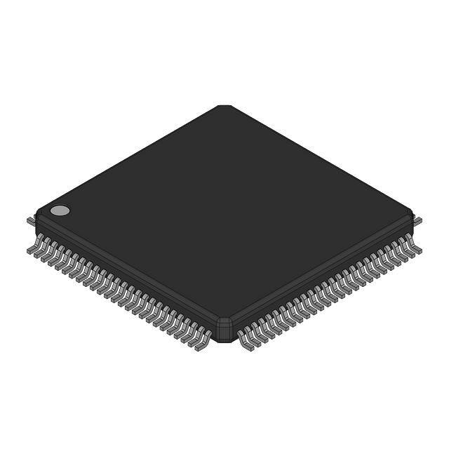
100-pin TQFP Package for Compact LCD
Module
Tolerates 4 kV HBM ESD for LVDS Pins and
2 kV HBM for Others
Improved Jitter Tolerance
description
The SN75LVDS88B (LVDS panel timing controller) integrates a Flatlink signal interface with a TFT LCD timing
controller. It resides in the LCD panel and provides interface between the graphic controller and a TFT LCD
panel.
The SN75LVDS88B accepts host data through 3 pairs of inputs (18-bits) making up the LVDS bus, which is a
low-EMI high-throughput interface. SN75LVDS88B then reformats the received image data into a specific data
format and synchronous timing suitable for driving LCD panel column and row drivers. This device supports
XGA resolution.
The SN75LVDS88B is easily configured by several selection terminals and is equipped with default timing
specifications to support mainstream gate and source drivers on the market.
block diagram
Data Alignment
Flatlink
(18-bit)
Source
Data
Format
SYNC
CTRL
Interface
Timing
Signal
Generator
Please be aware that an important notice concerning availability, standard warranty, and use in critical applications of
Texas Instruments semiconductor products and disclaimers thereto appears at the end of this data sheet.
Flatlink is a trademark of Texas Instruments.
Copyright 2001, Texas Instruments Incorporated
PRODUCTION DATA information is current as of publication date.
Products conform to specifications per the terms of Texas Instruments
standard warranty. Production processing does not necessarily include
testing of all parameters.
POST OFFICE BOX 655303
• DALLAS, TEXAS 75265
1
�SN75LVDS88B
TFT LCD PANEL TIMING CONTROLLER
WITH LVDS INTERFACE
SLLS407C – FEBRUARY 2000 – REVISED MAY 2001
pin assignment
1
2
3
4
5
6
7
8
9
10
11
12
13
14
15
16
17
18
19
20
21
22
23
24
25
SN75LVDS88B
EG4
EG3
VDDIO
EG2
EG1
VSSIO
EG0
EB5(ER5)
VDDIO
EB4(ER4)
EB3(ER3)
VSSIO
EB2(ER2)
EB1(ER1)
VDDIO
EB0(ER0)
EPOL
VSSIO
CLK
VDDIO
SP
OR5(OB3)
VSSIO
OR4(OB4)
OR3(OB3)
26
27
28
29
30
31
32
33
34
35
36
37
38
39
40
41
42
43
44
45
46
47
48
49
50
MODE2
TP1
CPV
VSS
STV
OE1
REV_E
VDD
REV_O
OE2
TP2
VSSIO
CLK
VDDIO
TEST2
ER5(EB5)
VSSIO
ER4(EB4)
ER3(EB3)
VDDIO
ER2(EB2)
ER1(EB1)
VSSIO
ER0(EB0)
EG5
100
99
98
97
96
95
94
93
92
91
90
89
88
87
86
85
84
83
82
81
80
79
78
77
76
TEST1
MODE1
NC
DBS
VSS
POLEN
VDDA
RSTZ
GNDA
GND1
NC
NC
CLKP
CLKM
A2P
A2M
A1P
A1M
A0P
A0M
GNDD
SHTDN
VDDD
NC
NC
TQFP PACKAGE
(TOP VIEW)
2
POST OFFICE BOX 655303
• DALLAS, TEXAS 75265
75
74
73
72
71
70
69
68
67
66
65
64
63
62
61
60
59
58
57
56
55
54
53
52
51
VDD
OPOL
VSS
OB0(OR0)
VDD
OB1(OR1)
OB2(OR2)
VSSIO
OB3(OR3)
OB4(OR4)
VDDIO
OB5(OR5)
OG0
VSSIO
OG1
OG2
VDDIO
OG3
OG4
VSSIO
OG5
OR0(OB0)
VDDIO
OR1(OB1)
OR2(OB2)
�SN75LVDS88B
TFT LCD PANEL TIMING CONTROLLER
WITH LVDS INTERFACE
SLLS407C – FEBRUARY 2000 – REVISED MAY 2001
Terminal Functions
TERMINAL
NAME
NO.
I/O
DESCRIPTION
A0M/A0P
81,82
I
A1M/A1P
83, 84
I
Flatlink 1st data pair
Flatlink 2nd data pair
A2M/A2P
85, 86
I
Flatlink 3rd data pair
CLK
44
O
CD bus clock
CLK
13
O
CD bus clock (180 degree out of phase)
87, 88
I
Flatlink clock pair
CPV
3
O
Gate driver clock
DBS
97
I
Data bus sequence
CLKM/CLKP
EPOL
42
O
Even RGB data stream polarity indicator
ER0..ER5
(EB0)..(EB5)
24, 22, 21,
19, 18, 16
O
Even red (blue) data bus, controlled by DBS Pin, 0 = red, 1 = blue
(ER0)..(ER5)
EB0..EB5
41,39,38
36,35,33
O
Even blue (red) data bus, controlled by DBS Pin, 0 = blue, 1 = red
GND1
91
P
PLL ground for LVDS
MODE1
99
I
Default timing selection pin 1
MODE2
1
I
Default timing selection pin 2
76, 77, 89, 90, 98
NC
OE1, OE2
6, 10
O
Gate driver output enable
OG0..OG5
63, 61, 60,
58, 57, 55
O
Odd green data bus
74
O
Odd RGB data stream polarity indicator
OR0..OR5
(OB0)..(OB5)
54, 52, 51,
50, 49, 47
O
Odd red (blue) data bus, controlled by DBS Pin, 0 = red, 1 = blue
(OR0)..(OR5)
OB0..OB5
72, 70, 69
67, 66, 64
O
Odd blue (red) data bus, controlled by DBS Pin, 0 = blue, 1 = red
NC
OPOL
NC terminals
POLEN
95
I
Output data polarity control enable /disable
REV_E
7
O
CD line/dot inversion control signal
REV_O
9
O
CD line/dot inversion control signal (180 degree of phase)
RSTZ
93
I
Reset, active low
SHTDN
79
I
System shutdown control, active low
SP
46
O
Data bus starting pulse
STV
TEST1, TEST2
TP1, TP2
5
O
100, 15
I
Gate driver starting pulse
Test points†
2, 11
O
CD output control signal
VDDA
94
P
PLL power for LVDS
GNDA
92
P
Analog ground for LVDS
VDDD
78
P
Digital power supply for LVDS
GNDD
80
P
Digital power ground for LVDS
VDD
8,71,75
P
Digital power
VSS
4,73,96
P
Digital ground
VDDIO
14, 20, 28, 34,
40, 45, 53, 59, 65
P
I/O power
VSSIO
12, 17, 23, 31,
37, 43, 48, 56,
62, 68
P
I/O ground
† Terminals must be connected to ground.
POST OFFICE BOX 655303
• DALLAS, TEXAS 75265
3
�SN75LVDS88B
TFT LCD PANEL TIMING CONTROLLER
WITH LVDS INTERFACE
SLLS407C – FEBRUARY 2000 – REVISED MAY 2001
options
output control
PIN NAME
PIN NO
NO.
INTERNAL CONNECTION
REQUIRED
DESCRIPTION
SUGGESTED
MODE1
MODE2
99
1
Pullup
Pulldown
Default timing selection pin 1
Default timing selection pin 2
POLEN
95
Pulldown
0 = Output data reverse disable
1 = Output data reverse enable
DBS
97
Pulldown
Data bus sequence
0 = normal (RGB)
1 = reverse (BGR)
NOTE: NC pin 76 is internally pulldown and NC pins 77 and 98 are internally pullup.
absolute maximum ratings over operating free-air temperature (unless otherwise noted)†
Supply voltage range, VCC‡ . . . . . . . . . . . . . . . . . . . . . . . . . . . . . . . . . . . . . . . . . . . . . . . . . . . . . . . . . –0.5 V to 4 V
Voltage range at any terminal . . . . . . . . . . . . . . . . . . . . . . . . . . . . . . . . . . . . . . . . . . . . . . . . . –0.5 V to VCC + 0.5 V
Continuous power dissipation . . . . . . . . . . . . . . . . . . . . . . . . . . . . . . . . . . . . . . . . . See Dissipation Rating Table
Storage temperature range, Tstg . . . . . . . . . . . . . . . . . . . . . . . . . . . . . . . . . . . . . . . . . . . . . . . . . . . –65°C to 150°C
Electrostatic discharge: Class 3 A . . . . . . . . . . . . . . . . . . . . . . . . . . . . . . . . . . . . . . . . . . . . . . . . . . . . . . . . . . 4 kV
Class 2 B . . . . . . . . . . . . . . . . . . . . . . . . . . . . . . . . . . . . . . . . . . . . . . . . . . . . . . . . . 200 V
Lead temperature 1,6 mm (1/16 inch) from case for 10 seconds . . . . . . . . . . . . . . . . . . . . . . . . . . . . . . . 260°C
† Stresses beyond those listed under “absolute maximum ratings” may cause permanent damage to the device. These are stress ratings only, and
functional operation of the device at these or any other conditions beyond those indicated under “recommended operating conditions” is not
implied. Exposure to absolute-maximum-rated conditions for extended periods may affect device reliability.
‡ All voltage values are with respect to the GND terminals unless otherwise noted.
DISSIPATION RATING TABLE
PACKAGE
TA ≤ 25°C
POWER RATING
PFD
RDD
OPERATING FACTOR§
ABOVE TA = 25°C
TA = 70°C
POWER RATING
1.548 W
12 mW
1.012 W
1.089 W
8.4 mW
0.712 W
§ This is the inverse of the junction-to-ambient thermal resistance when board-mounted and with
no air flow.
4
POST OFFICE BOX 655303
• DALLAS, TEXAS 75265
�SN75LVDS88B
TFT LCD PANEL TIMING CONTROLLER
WITH LVDS INTERFACE
SLLS407C – FEBRUARY 2000 – REVISED MAY 2001
recommended operating conditions
MIN
NOM
3
3.3
Supply voltage, VCC
High-level input voltage, VIH
Low-level input voltage, VIL
MAX
UNIT
3.6
V
2
SHTDN
V
0.8
Magnitude of differential input voltage, VID
0.1
|V
ID
2
Common–mode input voltage, VIC
Operating free-air temperature, TA
0.6
|
V
|V
ID
2
2.4 –
0
|
V
°C
70
electrical characteristics over recommended operating free-air temperature range (unless
otherwise noted)
PARAMETER
VIT+
VIT–
TEST CONDITIONS
MIN
TYP†
Positive-going differential input voltage threshold
Negative-going differential input voltage threshold
IIH
IIL
Current (average)
High-level input current (SHTDN)
Low-level input current (SHTDN)
UNIT
100
mV
–100
mV
Disabled, all inputs to ground
ICC
MAX
360
Enabled, AnP at 1 V and
AnM at 1.4 V,
tC = 15.38 ns
80
Enabled, CL = 8 pF,
Grayscale pattern , tC = 15.38 ns
100
Enabled, CL = 8 pF,
Worst-case pattern, tC = 15.38 ns
120
VIH = VCC
VIL = 0 V
µA
mA
±20
µA
±20
µA
IIN
Input current (A inputs)
0 V < VI < 2.4 V
±20
µA
IOZ
High-impedance output current
VO = 0 V or VCC
±10
µA
† All typical values are at VCC = 3.3 V, TA = 25°C.
‡ The algebraic convention, in which the less-positive (more-negative) limit is designated minimum, is used in this data sheet for the negative-going
input voltage threshold only.
timing requirements
MIN
tc§
tsu/th
Input clock period
14.7
Input set up or hold time
550
TYP
MAX
UNIT
31.25
ns
ps
§ tc is defined as the mean duration of a minimum of 32,000 clock periods.
output buffer rating
MIN
TYP
MAX
UNIT
STV, SP
4
mA
CLK, CLK
8
mA
Data bus and remaining outputs
4
mA
POST OFFICE BOX 655303
• DALLAS, TEXAS 75265
5
�SN75LVDS88B
TFT LCD PANEL TIMING CONTROLLER
WITH LVDS INTERFACE
SLLS407C – FEBRUARY 2000 – REVISED MAY 2001
switching characteristics
PARAMETER
TEST CONDITIONS
tdr1
tdf1
Input clock rising to output clock rising delay
tsu1
th1
Data setup time, E/O RGB to CLK↑
Input clock rising to output clock falling delay
CL = 80 pF
CL = 80 pF
Data hold time, CLK↑ to E/O RGB
t(RSKM)
Receiver input skew margin, See Note 1
ten
tdis
Enable time, SHTDN to phase lock
tsu2
th2
SP setup time
tc = 15.38 ns (+0.2%),
Input clock jitter < 50 ps, See Note 2
MIN
Csp = 10 pF
MAX
UNIT
40
ns
10
40
ns
10
20
ns
10
20
ns
550
Disable time, SHTDN to off state
SP pulse hold time
TYP
10
700
ps
1
ms
250
ns
10
20
ns
10
20
ns
NOTES: 1. tRSKM is the timing margin available to allocate to the transmitter and interconnection skews and clock jitter. The value of this
tc
parameter at clock periods other than 15.38 ns can be calculated from t
–300 ps.
RSKM
14
2. | Input clock jitter | is the magnitude of the change in the input clock period.
+
PARAMETER MEASUREMENT INFORMATION
CLKM/P
tdr1
tdr1
CLK
tsu1
th
tsu2
th2
RGB
SP
Figure 1. Output Setup and Hold Time
6
POST OFFICE BOX 655303
• DALLAS, TEXAS 75265
�SN75LVDS88B
TFT LCD PANEL TIMING CONTROLLER
WITH LVDS INTERFACE
SLLS407C – FEBRUARY 2000 – REVISED MAY 2001
PARAMETER MEASUREMENT INFORMATION
reference timing diagrams
horizontal timing
DE
E/OSP
O/ERGB
CPV
TP1
TP2
OE1
OE2
REV
vertical timing
DE
TP
Figure 2. Typical Output Waveform
POST OFFICE BOX 655303
• DALLAS, TEXAS 75265
7
�SN75LVDS88B
TFT LCD PANEL TIMING CONTROLLER
WITH LVDS INTERFACE
SLLS407C – FEBRUARY 2000 – REVISED MAY 2001
PARAMETER MEASUREMENT INFORMATION
functional description
Flatlink
The core of the Flatlink is TIs original 86A LVDS receiver, which has three data channels for the 18-bit color plus
one clock channel.
data alignment
The data alignment block supports dual bus, dual port column driver configuration. When interfacing a 2-port
column driver, the controller arranges pixels in odd and even order, then distributes them to odd and even buses
and each connects to either of the driver ports. Under this setup, the controller outputs one clock, one or two
data polarities (depends on driver), and one inverse ( support line inversion) signal to the drivers.
output formatting
The output formatting provides several functions to reduce EMI, noise, and timing delay arrangement. These
functions are controllable through some optional pins. See the registers and options section for reference.
D
D
Reverse Polarity Generation
When enabled, this function generates polarity indication signals. This occurs when the number of
transitions in the output data bus exceeds 18-bits compared to the previous output under normal polarity.
The polarity signal will be active and the output will be the opposite polarity to reduce transition.
Line Inversion
When enabled, the REV_O and REV_E terminals will output the same line inversion control signals but in
opposite polarities.
timing control
D
D
D
D
D
D
8
Horizontal Starting pulses
ESP and OSP terminals are used as the horizontal starting pulses output pins. Their outputs are one HCLK
period ahead of the RGB data stream
Horizontal Clock
ECLK and OCLK terminals are responsible for the clock pulses, based on the XGA resolution when its
frequency is at 32.5 MHz.
CD Data Latch Pulse
TP1 and TP2 provide the column driver input latch and output enable signals.
Gate Driver Clock
The CPV terminal output the clock pulses to the gate drivers as the horizontal sync timing in its CRT counter
part.
Gate Driver Starting Pulse
The vertical starting pulse automatically generates at the start of every frame.
Gate Driver Output Enable
The OE1 and OE2 terminals provide the gate output enable signals.
POST OFFICE BOX 655303
• DALLAS, TEXAS 75265
�SN75LVDS88B
TFT LCD PANEL TIMING CONTROLLER
WITH LVDS INTERFACE
SLLS407C – FEBRUARY 2000 – REVISED MAY 2001
PARAMETER MEASUREMENT INFORMATION
functional description (continued)
vertical/horizontal reference generator
This block provides vertical and horizontal reference points for timing control. Vsync, Hsync, and ENAB signals,
along with the auto detection function, determine when the video from the host is valid.
power-up procedure
Due to the uncertainty of registers and counters in the driver, SN75LVDS88B combines the input from both reset
and Vsync to blank the output and simultaneously resets the content of drivers (see Figure 3).
VSYNC
RSTZ
OE
Figure 3. Reset Waveform
It is recommended that the following circuit be used to ensure the device is reset for more than 5 ms after power
up.
10 kΩ
RSTZ
4.7 µF
POST OFFICE BOX 655303
• DALLAS, TEXAS 75265
9
�SN75LVDS88B
TFT LCD PANEL TIMING CONTROLLER
WITH LVDS INTERFACE
SLLS407C – FEBRUARY 2000 – REVISED MAY 2001
APPLICATION INFORMATION
SN75LVDS88B
ERGB
ORGB
REV_E/O
CLK
SP
CD1
CD2
CD3
CD4
Figure 4. Application Block Diagram
CLK
SP
ORGB
1
3
5
7
9
11
ERGB
2
4
6
8
10
12
Figure 5. Data Output Format
10
POST OFFICE BOX 655303
• DALLAS, TEXAS 75265
�SN75LVDS88B
TFT LCD PANEL TIMING CONTROLLER
WITH LVDS INTERFACE
SLLS407C – FEBRUARY 2000 – REVISED MAY 2001
MECHANICAL DATA
PFD (S-PQFP-G100)
PowerPAD PLASTIC QUAD FLATPACK (DIE DOWN)
0,27
0,17
0,50
75
0,08 M
51
50
76
Thermal Pad
(see Note D)
26
100
0,13 NOM
1
25
12,00 TYP
Gage Plane
14,20
SQ
13,80
16,20
SQ
15,80
1,05
0,95
0,25
0,15
0,05
0°– 7°
0,75
0,45
Seating Plane
0,08
1,20 MAX
4146930/A 12/97
NOTES: A.
B.
C.
D.
All linear dimensions are in millimeters.
This drawing is subject to change without notice.
Body dimensions do not include mold flash or protrusion.
The package thermal performance may be enhanced by attaching an external heatsink to the thermal pad.
This pad is electrically and thermally connected to the backside of the die and possibly selected leads.
E. Falls within JEDEC MS-026
PowerPAD is a trademark of Texas Instruments Incorporated.
POST OFFICE BOX 655303
• DALLAS, TEXAS 75265
11
�MECHANICAL DATA
MPQF080– NOVEMBER 1998
MECHANICAL DATA
RDD (S-PQFP-G100)
PowerPAD PLASTIC QUAD FLATPACK (DIE DOWN)
0,28
0,16
0,50
75
0,08 M
51
50
76
Thermal Pad
(See Note D)
26
100
0,13 NOM
1
25
12,00 TYP
Gage Plane
14,10
SQ
13,90
16,20
SQ
15,80
0,25
0,15
0,05
0,85
0,75
0° – 5°
0,70
0,30
Seating Plane
1,00 MAX
0,10
4146938/A 10/98
NOTES: A.
B.
C.
D.
All linear dimensions are in millimeters.
This drawing is subject to change without notice.
Body dimensions do not include mold flash or protrusion
The package thermal performance may be enhanced by attaching an external heatsink to the thermal pad.
This pad is electrically and thermally connected to the backside of the die and possibly selected leads.
E. Falls within JEDEC MS-026
For the latest package information, go to http://www.ti.com/sc/docs/package/pkg_info.htm
PowerPAD is a trademark of Texas Instruments Incorporated.
12
POST OFFICE BOX 655303
• DALLAS, TEXAS 75265
�PACKAGE OPTION ADDENDUM
www.ti.com
24-Jun-2005
PACKAGING INFORMATION
Orderable Device
Status (1)
Package
Type
Package
Drawing
Pins Package Eco Plan (2)
Qty
SN75LVDS88BPFD
ACTIVE
HTQFP
PFD
100
SN75LVDS88BRDD
OBSOLETE
HVQFP
RDD
100
90
Lead/Ball Finish
Green (RoHS &
no Sb/Br)
CU NIPDAU
TBD
Call TI
MSL Peak Temp (3)
Level-3-260C-168 HR
Call TI
(1)
The marketing status values are defined as follows:
ACTIVE: Product device recommended for new designs.
LIFEBUY: TI has announced that the device will be discontinued, and a lifetime-buy period is in effect.
NRND: Not recommended for new designs. Device is in production to support existing customers, but TI does not recommend using this part in
a new design.
PREVIEW: Device has been announced but is not in production. Samples may or may not be available.
OBSOLETE: TI has discontinued the production of the device.
(2)
Eco Plan - The planned eco-friendly classification: Pb-Free (RoHS) or Green (RoHS & no Sb/Br) - please check
http://www.ti.com/productcontent for the latest availability information and additional product content details.
TBD: The Pb-Free/Green conversion plan has not been defined.
Pb-Free (RoHS): TI's terms "Lead-Free" or "Pb-Free" mean semiconductor products that are compatible with the current RoHS requirements
for all 6 substances, including the requirement that lead not exceed 0.1% by weight in homogeneous materials. Where designed to be soldered
at high temperatures, TI Pb-Free products are suitable for use in specified lead-free processes.
Green (RoHS & no Sb/Br): TI defines "Green" to mean Pb-Free (RoHS compatible), and free of Bromine (Br) and Antimony (Sb) based flame
retardants (Br or Sb do not exceed 0.1% by weight in homogeneous material)
(3)
MSL, Peak Temp. -- The Moisture Sensitivity Level rating according to the JEDEC industry standard classifications, and peak solder
temperature.
Important Information and Disclaimer:The information provided on this page represents TI's knowledge and belief as of the date that it is
provided. TI bases its knowledge and belief on information provided by third parties, and makes no representation or warranty as to the
accuracy of such information. Efforts are underway to better integrate information from third parties. TI has taken and continues to take
reasonable steps to provide representative and accurate information but may not have conducted destructive testing or chemical analysis on
incoming materials and chemicals. TI and TI suppliers consider certain information to be proprietary, and thus CAS numbers and other limited
information may not be available for release.
In no event shall TI's liability arising out of such information exceed the total purchase price of the TI part(s) at issue in this document sold by TI
to Customer on an annual basis.
Addendum-Page 1
�IMPORTANT NOTICE
Texas Instruments Incorporated and its subsidiaries (TI) reserve the right to make corrections, modifications,
enhancements, improvements, and other changes to its products and services at any time and to discontinue
any product or service without notice. Customers should obtain the latest relevant information before placing
orders and should verify that such information is current and complete. All products are sold subject to TI’s terms
and conditions of sale supplied at the time of order acknowledgment.
TI warrants performance of its hardware products to the specifications applicable at the time of sale in
accordance with TI’s standard warranty. Testing and other quality control techniques are used to the extent TI
deems necessary to support this warranty. Except where mandated by government requirements, testing of all
parameters of each product is not necessarily performed.
TI assumes no liability for applications assistance or customer product design. Customers are responsible for
their products and applications using TI components. To minimize the risks associated with customer products
and applications, customers should provide adequate design and operating safeguards.
TI does not warrant or represent that any license, either express or implied, is granted under any TI patent right,
copyright, mask work right, or other TI intellectual property right relating to any combination, machine, or process
in which TI products or services are used. Information published by TI regarding third-party products or services
does not constitute a license from TI to use such products or services or a warranty or endorsement thereof.
Use of such information may require a license from a third party under the patents or other intellectual property
of the third party, or a license from TI under the patents or other intellectual property of TI.
Reproduction of information in TI data books or data sheets is permissible only if reproduction is without
alteration and is accompanied by all associated warranties, conditions, limitations, and notices. Reproduction
of this information with alteration is an unfair and deceptive business practice. TI is not responsible or liable for
such altered documentation.
Resale of TI products or services with statements different from or beyond the parameters stated by TI for that
product or service voids all express and any implied warranties for the associated TI product or service and
is an unfair and deceptive business practice. TI is not responsible or liable for any such statements.
Following are URLs where you can obtain information on other Texas Instruments products and application
solutions:
Products
Applications
Amplifiers
amplifier.ti.com
Audio
www.ti.com/audio
Data Converters
dataconverter.ti.com
Automotive
www.ti.com/automotive
DSP
dsp.ti.com
Broadband
www.ti.com/broadband
Interface
interface.ti.com
Digital Control
www.ti.com/digitalcontrol
Logic
logic.ti.com
Military
www.ti.com/military
Power Mgmt
power.ti.com
Optical Networking
www.ti.com/opticalnetwork
Microcontrollers
microcontroller.ti.com
Security
www.ti.com/security
Telephony
www.ti.com/telephony
Video & Imaging
www.ti.com/video
Wireless
www.ti.com/wireless
Mailing Address:
Texas Instruments
Post Office Box 655303 Dallas, Texas 75265
Copyright 2005, Texas Instruments Incorporated
�


 工商网监
湘ICP备2023018690号
工商网监
湘ICP备2023018690号
