SN75LVDT1422
www.ti.com
SLLS653 – JUNE 2005
14-BIT FULL DUPLEX SERIALIZER/DESERIALIZER
FEATURES
•
•
•
•
•
•
•
•
•
10 MHz to 100 MHz Shift Clock Support
175 Mbytes/sec In TX/RX Modes
Reduces Cable Size, Cost, and System EMI
Bidirectional Data Communication
Total Power < 360 mW Typ at 100-MHz Worst
Case Pattern
Power-Down Mode: < 500 µW Typ
No External Components Required for PLL
Inputs and Outputs Compatible with
TIA/EIA-644 LVDS Standard
ESD Rating > 5 kV (HBM)
•
•
•
Integrated Termination Resistor
Supports Spread Spectrum Clocking
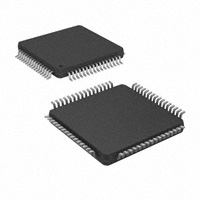
64-Pin TQFP Package (PAG)
APPLICATIONS
•
•
•
Flash Memory Cards
Plain Paper Copiers
Printers
DESCRIPTION
The SN75LVDT1422 Full Duplex Serializer/Deserializer incorporates a 14-bit serializer and a 14-bit deserializer.
Operation of the serializer is independent of the operation of the deserializer. The 14-bit serializer accepts 14
TTL input lines and generates 2 LVDS high-speed serial streams plus one LVDS clock signal. The 14-bit
deserializer accepts 3 LVDS input signals (2 high-speed serial streams and one LVDS clock signal) and drives
out 14 TTL data signals plus one TTL clock.
The serializer loads 14 data bits into registers upon the rising or falling edge of the input clock signal (CLK IN).
Rising or falling edge operation can be selected via the R/F select pin for the transmitter only. The frequency of
CLK IN is multiplied seven times and then used to unload the data registers in 7-bit slices. The two high-speed
serial streams and a phase-locked clock (TCLK±) are then output to LVDS output drivers. The frequency of
TCLK± is the same as the input clock, CLK IN.
The deserializer accepts data on two high-speed LVDS data lines. High-speed data is received and loaded into
registers at the rate seven times the LVDS input clock (RCLK±). The data is then unloaded to a 14-bit wide
LVTTL parallel bus at the RCLK± rate. The SN75LVDT1422 presents valid data on the falling edge of the output
clock (CLK OUT).
The SN75LVDT1422 provides three termination resistors for the differential LVDS inputs thus minimizing cost,
and board space, while providing better overall signal integrity (SI). The data bus appears the same at the input
to the transmitter and output of the receiver with the data transmission transparent to the user(s). The only user
interventions are as follows:
Possible use of the TX ENABLE and RX ENABLE feature. Both the TX and RX ENABLE circuits are
active-high inputs that independently enable the serializer and deserializer. When TX is disabled, the LVDS
outputs go to high impedance. When RX is disabled, the TTL outputs go to a known low state.
The SN75LVDT1422 is characterized for operation over the free-air temperature range of –10°C to 70°C.
Please be aware that an important notice concerning availability, standard warranty, and use in critical applications of Texas
Instruments semiconductor products and disclaimers thereto appears at the end of this data sheet.
PRODUCTION DATA information is current as of publication date.
Products conform to specifications per the terms of the Texas
Instruments standard warranty. Production processing does not
necessarily include testing of all parameters.
Copyright © 2005, Texas Instruments Incorporated
�SN75LVDT1422
www.ti.com
SLLS653 – JUNE 2005
These devices have limited built-in ESD protection. The leads should be shorted together or the device
placed in conductive foam during storage or handling to prevent electrostatic damage to the MOS gates.
FUNCTIONAL BLOCK DIAGRAM
TX ENABLE
TA+
TA0−TA6
IN
7
OUT
TA−
Parallel In
to
Serial Out
R/F
TB0−TB6
IN
7
TB+
OUT
TB−
>CLK
TCLK+
CLK IN
PLL
TCLK−
RA+
RA0−RA6
IN
OUT
7
100 �
RA−
Serial In
to
Parallel Out
RB0−RB6
7
RB+
IN
OUT
100 �
RB−
CLK<
RCLK+
CLK OUT
PLL
100 �
RCLK−
RX ENABLE
2
�SN75LVDT1422
www.ti.com
SLLS653 – JUNE 2005
RX PLL GND
RX PLL VCC
RA2
RA1
RA0
CLK OUT
RX GND
RX ENABLE
RX LVDS VCC
RA+
RA−
RCLK+
RCLK−
RB+
RB−
RX LVDS GND
PAG PACKAGE
(TOP VIEW)
64 63 62 61 60 59 58 57 56 55 54 53 52 51 50 49
1
48
2
47
3
46
4
45
5
44
6
43
7
42
8
41
9
40
10
39
11
38
12
37
13
36
14
35
15
34
16
33
TX ENABLE
TX LVDS VCC
TB−
TB+
TCLK−
TCLK+
TA−
TA+
TX LVDS GND
TX PLL GND
TX PLL VCC
R/F
TX GND
TB6
TB5
TB4
17 18 19 20 21 22 23 24 25 26 27 28 29 30 31 32
CLK IN
TX GND
TA0
TA1
TA2
TX VCC
TA3
TA4
TA5
TA6
TX VCC
TB0
TB1
TB2
TB3
TX VCC
RX VCC
RA3
RA4
RA5
RA6
RX GND
RX VCC
RB0
RB1
RB2
RB3
RX VCC
RB4
RB5
RB6
RX GND
3
�SN75LVDT1422
www.ti.com
SLLS653 – JUNE 2005
TERMINAL FUNCTIONS
TERMINAL
NAME
NO.
TYPE
CLK IN
17
CLK OUT
61
R/F
37
LVTTL Input
Input clock triggering edge select.
High: Rising edge
Low: Falling edge
57, 56
LVDS Input
LVDS Data inputs
RA+, RA–
62, 63, 64, 2,
3, 4, 5
RA[0:6]
RB+, RB–
53, 52
8, 9, 10, 11,
13, 14, 15
RB[0:6]
RCLK+, RCLK–
RX ENABLE
RX GND
LVTTL Input
DESCRIPTION
CMOS/LVTTL Clock input
LVTTL Output LVTTL Clock output
LVTTL Output Single-ended data outputs
LVDS Input
LVDS Data inputs
LVTTL Output Single-ended data outputs
55, 54
LVDS Input
LVDS Clock inputs
59
LVTTL Input
Receiver enable: When asserted (low input), the receiver outputs go to a known
low state.
6, 16, 60
Ground pins for RX TTL outputs
RX LVDS GND
51
Ground pin for RX LVDS inputs
RX LVDS VCC
58
RX PLL GND
50
RX PLL VCC
49
Power supply pin for PLL RX circuitry
1, 7, 12
Power supply pins for RX TTL outputs
RX VCC
TA+, TA–
TA[0:6]
Power Supply
Power supply pin for RX LVDS inputs
Ground pin for PLL RX circuitry
41, 42
LVDS Output
LVDS Data outputs
19, 20, 21, 23, 24,
25, 26
LVTTL Input
Single-ended data inputs
45, 46
LVDS Output
LVDS Data outputs
28, 29, 30, 31,
33,34, 35
LVTTL Input
Single-ended data inputs
43, 44
LVDS Output
LVDS Clock outputs
48
LVTTL Input
Transmitter enable: When asserted (low input), the driver outputs are
high-impedance.
TB+, TB–
TB[0:6]
TCLK+, TCLK–
TX ENABLE
TX GND
18, 36
Ground pins for TX TTL inputs
TX LVDS GND
40
TX LVDS VCC
47
TX PLL GND
39
TX PLL VCC
38
Power supply pin for PLL TX circuitry
22, 27, 32
Power supply pins for TX TTL inputs
TX VCC
Ground pin for TX LVDS outputs
Power Supply
Power supply pin for TX LVDS outputs
Ground pin for PLL TX circuitry
ORDERING INFORMATION (1)
(1)
4
PRODUCT
PACKAGE
ORDERING NUMBER
SN75LVDT1422
TQFP (PAG)
SN75LVDT1422
For the most current package and ordering information, see the Package Option Addendum at the end of this document, or see the TI
website at www.ti.com.
�SN75LVDT1422
www.ti.com
SLLS653 – JUNE 2005
ABSOLUTE MAXIMUM RATINGS
(1)
UNIT
Supply voltage range, VCC
(2)
–0.5 V to 4 V
Voltage range at any terminal
–0.3 V to VCC + 0.3 V
±5 kV
Human Body Model (3) (All pins)
Electrostatic discharge
Machine Model
(4)(All
±200 V
pins)
±500 V
Charged-Device Model (5) (All pins)
Continuous power dissipation
See Dissipation Rating Table
Storage temperature range
(1)
(2)
(3)
(4)
(5)
–65°C to 125°C
Stresses beyond those listed under absolute maximum ratings may cause permanent damage to the device. These are stress ratings
only and functional operation of the device at these or any other conditions beyond those indicated under recommended operating
conditions is not implied. Exposure to absolute-maximum-rated conditions for extended periods may affect device reliability.
All voltage values are with respect to the GND terminals
In accordance with JEDEC Standard 22, Test Method A114-A.
In accordance with JEDEC Standard 22, Test Method A115.
In accordance with JEDEC Standard 22, Test Method C101.
DISSIPATION RATINGS
(1)
(2)
(3)
PACKAGE
CIRCUIT
BOARD MODEL
TA≤ 25°C
DERATING FACTOR (1)
ABOVE TA = 25°C
TA = 70°C
POWER RATING
TQFP (PAG)
Low-K (2)
813 mW
8.13 mW/°C
448 mW
TQFP (PAG)
High-K (3)
1076 mW
10.76 mW/°C
592 mW
This is the inverse of the junction-to-ambient thermal resistance when board-mounted and with no air flow.
In accordance with the Low-K thermal metric definitions of EIA/JESD51-2.
In accordance with the High-K thermal metric definitions of EIA/JESD51-6.
THERMAL CHARACTERISTICS
PARAMETER
TEST CONDITIONS
VALUE
RθJB
Junction-to-board thermal resistance
69.5
RθJC
Junction-to-case thermal resistance
39.2
PD
Device power dissipation
UNIT
°C/ W
Typical
VCC = 3.3 V, TA = 25°C, f = 100 MHz
357.4
Maximum
VCC= 3.6 V, TA = 70°C , f = 100 MHz
455.8
mW
RECOMMENDED OPERATING CONDITIONS
MIN
NOM
MAX
VCC
Supply voltage
3
3.3
3.6
UNIT
V
VIH
High-level input voltage
2
VCC
V
VIL
Low-level input voltage
GND
0.8
V
|VID|
Magnitude of differential input voltage
0.1
0.6
V
VIC
Common-mode input voltage range, receiver
|VID|/2
2.4 – |VID|/2
V
TA
Operating free-air temperature
–10
70
°C
VN
Supply noise voltage, VCC
–50
50
mV
fc
Clock frequency
10
100
MHz
5
�SN75LVDT1422
www.ti.com
SLLS653 – JUNE 2005
RECEIVER ELECTRICAL CHARACTERISTICS
over recommended operating conditions (unless otherwise noted)
PARAMETER
TEST CONDITIONS
MIN
TYP (1) MAX
Positive-going differential input threshold voltage
VIT–
Negative-going differential input threshold voltage
VOH
High-level output voltage
IOH = –4 mA
VOL
Low-level output voltage
IOL = 4 mA
VIK
Input clamp voltage
II = –18 mA
–1.5
II
Input current with integrated termination
VI = 0 V or 2.4 V, VCC = 3.6 V
–45
45
µA
II(OFF)
Power-off input current
VCC = 0 V, VI = 2.4 V
–10
10
µA
RT
Termination resistance
VID = 100 mV, VIC = 0.05 V to 2.4 V
132
Ω
Ci
Input capacitance
(1)
100
UNIT
VIT+
–100
mV
2.4
V
0.4
90
mV
–0.8
110
V
V
2
pF
All typical values are at VCC = 3.3 V, TA = 25°C.
TRANSMITTER ELECTRICAL CHARACTERISTICS
over recommended operating conditions (unless otherwise noted)
PARAMETER
TEST CONDITIONS
RL = 100 Ω
MIN
TYP (1)
MAX
UNIT
250
365
450
mV
–35
35
mV
1.125
1.375
–35
35
mV
80
mV
20
µA
10
µA
|VOD|
Differential output voltage magnitude
∆|VOD|
Change in differential output voltage magnitude between logic
states
VOC(SS)
Steady-state common-mode output voltage
∆VOC(SS)
Change in steady-state common-mode output voltage between
logic states
VOC(PP)
Peak-to-peak common-mode output voltage
IIH
High-level input current
VIH = 2 V
IIL
Low-level input current
VIL = 0.8 V
–10
VIK
Input clamp voltage
II = –18 mA
–1.5
VO+ or VO– = 0 V
–24
24
VOD = 0 V
–12
12
VCC = 0 V, VO = 2.4 V
–10
10
IOS
Short-circuit output current
IO(OFF)
Power-off output current
Ci
Input capacitance
(1)
30
–0.8
V
V
3
mA
µA
pF
All typical values are at VCC = 3.3 V, TA = 25°C.
TRANSMITTER SUPPLY CURRENT
PARAMETER
ICC
(1)
6
Supply current (worst case)
MIN TYP (1)
MAX
f = 10 MHz
17
23
f = 25 MHz
19
27
f = 40 MHz
22
30
f = 65 MHz
29
34
f = 85 MHz
34
45
f = 100 MHz
38
49
TEST CONDITIONS
See Figure 1 and Figure 2
All typical values are at VCC = 3.3 V, TA = 25°C.
UNIT
mA
�SN75LVDT1422
www.ti.com
SLLS653 – JUNE 2005
RECEIVER SUPPLY CURRENT
PARAMETER
ICC
(1)
Supply current (worst case)
MIN TYP (1)
MAX
f = 10 MHz
19
35
f = 25 MHz
27
42
f = 40 MHz
35
45
f = 65 MHz
49
69
f = 85 MHz
60
81
f = 100 MHz
69
90
MIN TYP (2)
MAX
UNIT
150
800
µA
TEST CONDITIONS
See Figure 1 and Figure 3
UNIT
mA
All typical values are at VCC = 3.3 V, TA = 25°C.
SUPPLY CURRENT (1)
PARAMETER
ICC(DIS)
(1)
(2)
Disable supply current
TEST CONDITIONS
TX/RX ENABLEs = GND
CMOS inputs have to connect to ground.
All typical values are at VCC = 3.3 V, TA = 25°C.
TRANSMITTER INPUT TIMING REQUIREMENTS
PARAMETER
tt(CLK)
Transition time, CLK IN
tc(CLK)
Input clock period, CLK IN
twH(CLK)
Pulse duration, clock high, CLK IN
twL(CLK)
Pulse duration, clock low, CLK IN
tt(EN)
Transition time, TX ENABLE, TAx/TBx
(1)
(2)
TEST CONDITIONS
See Figure 5
See Figure 6
MIN
TYP (1)
1.0
MAX
UNIT
6.0 (2)
ns
10
T
100
ns
0.35T
0.5T
0.65T
ns
0.35T
0.5T
0.65T
ns
6.0
ns
TYP (1)
MAX
UNIT
0.38
0.7
ns
ns
1.5
All typical values are at VCC = 3.3 V, TA = 25°C.
Regulate clock frequency lower than 50 MHz. tt(CLK)max = 1/f x 50% x 60%.
TRANSMITTER SWITCHING CHARACTERISTICS
PARAMETER
TEST CONDITIONS
MIN
tr
LVDS Rise time
See Figure 4
tf
LVDS Fall time
See Figure 4
0.38
0.7
t0
Output pulse position for bit 0
-0.8
0
0.8
t1
Output pulse position for bit 1
13.49
14.29
15.09
t2
Output pulse position for bit 2
27.77
28.57
29.37
t3
Output pulse position for bit 3
42.06
42.86
43.66
t4
Output pulse position for bit 4
56.34
57.14
57.94
t5
Output pulse position for bit 5
70.63
71.43
72.23
t6
Output pulse position for bit 6
84.91
85.71
86.51
t0
Output pulse position for bit 0
–0.45
0
0.45
t1
Output pulse position for bit 1
5.26
5.71
6.16
t2
Output pulse position for bit 2
10.98
11.43
11.83
t3
Output pulse position for bit 3
16.69
17.14
17.54
t4
Output pulse position for bit 4
22.41
22.86
23.26
t5
Output pulse position for bit 5
28.12
28.57
28.97
t6
Output pulse position for bit 6
33.84
34.29
34.69
(1)
f = 10 MHz, See Figure 12
f = 25 MHz, See Figure 12
ns
ns
All typical values are at VCC = 3.3 V, TA = 25°C.
7
�SN75LVDT1422
www.ti.com
SLLS653 – JUNE 2005
TRANSMITTER SWITCHING CHARACTERISTICS (continued)
PARAMETER
TEST CONDITIONS
MIN
TYP (1)
MAX
t0
Output pulse position for bit 0
–0.25
0
0.25
t1
Output pulse position for bit 1
3.32
3.57
3.82
t2
Output pulse position for bit 2
6.89
7.14
7.39
t3
Output pulse position for bit 3
10.46
10.71
10.96
t4
Output pulse position for bit 4
14.04
14.29
14.54
t5
Output pulse position for bit 5
17.61
17.86
18.11
t6
Output pulse position for bit 6
21.18
21.43
21.68
t0
Output pulse position for bit 0
–0.20
0
0.20
t1
Output pulse position for bit 1
2.00
2.20
2.40
t2
Output pulse position for bit 2
4.20
4.40
4.60
t3
Output pulse position for bit 3
6.39
6.59
6.79
t4
Output pulse position for bit 4
8.59
8.79
8.99
t5
Output pulse position for bit 5
10.79
10.99
11.19
t6
Output pulse position for bit 6
12.99
13.19
13.39
t0
Output pulse position for bit 0
–0.15
0
0.15
t1
Output pulse position for bit 1
1.53
1.68
1.83
t2
Output pulse position for bit 2
3.21
3.36
3.51
t3
Output pulse position for bit 3
4.89
5.04
5.19
t4
Output pulse position for bit 4
6.57
6.72
6.87
t5
Output pulse position for bit 5
8.25
8.40
8.55
t6
Output pulse position for bit 6
9.93
10.08
10.23
t0
Output pulse position for bit 0
-0.2
0
0.2
t1
Output pulse position for bit 1
1.23
1.43
1.63
t2
Output pulse position for bit 2
2.66
2.86
3.06
t3
Output pulse position for bit 3
4.09
4.29
4.49
t4
Output pulse position for bit 4
5.51
5.71
5.91
t5
Output pulse position for bit 5
6.94
7.14
7.34
t6
Output pulse position for bit 6
8.37
8.57
8.77
tsu
TAx/TBx Setup time to CLK IN
th
TAx/TBx Hold time to CLK IN
tpd(TCC)
CLK IN to TCLK± Propagation delay time
tjit(C-C)
TCLK± Clock cycle-to-cycle jitter
f = 40 MHz, See Figure 12
f = 65 MHz, See Figure 12
f = 85 MHz, See Figure 12
f = 100 MHz, See Figure 12
f = 85 MHz or 100 MHz, See Figure 6
See Figure 7 and Figure 8 (2)
1
UNIT
ns
ns
ns
ns
ns
0.25
f = 10 MHz
1.0
2.98
f = 25 MHz
1.38
3.21
f = 85 MHz
1.60
3.78
f = 100 MHz
1.63
3.95
f = 85 MHz or 100 MHz
50
ns
ps
f = 10 MHz
f = 25 MHz
SSCG
Spread Spectrum Clock support; Modulation frequency with a linear profile (3)
f = 40 MHz
100
f = 65 MHz
±2.5%/–5%
kHz
f = 85 MHz
f = 100 MHz
ten(TPLL) Phase lock loop enable time
See Figure 9
10
ms
tdis(T)
See Figure 11
100
ns
(2)
(3)
8
Transmitter disable time
Measure from CLK IN rising edge or falling edge to immediately crossing point of differential TCLK±, 50% duty cycle input clock is
assumed.
Care must be taken to ensure tsu and th are met so input data are sampling correctly. This SSCG parameter only shows the
performance of tracking spread spectrum clock applied to CLK IN pin, and reflects the result on TCLK+ and TCLK– pins.
�SN75LVDT1422
www.ti.com
SLLS653 – JUNE 2005
RECEIVER SWITCHING CHARACTERISTICS
PARAMETER
TEST CONDITIONS
CLK OUT
MIN
MAX
1.2
2.5
2.0
3.5
1.2
2.5
2.0
3.5
tr
CMOS/LVTTL Rise time
tf
CMOS/LVTTL Fall time
t0
Input strobe position for bit 0
0.45
0.84
1.23
t1
Input strobe position for bit 1
2.13
2.52
2.91
t2
Input strobe position for bit 2
3.81
4.20
4.59
t3
Input strobe position for bit 3
5.49
5.88
6.27
t4
Input strobe position for bit 4
7.17
7.56
7.95
t5
Input strobe position for bit 5
8.85
9.24
9.63
t6
Input strobe position for bit 6
10.53
10.92
11.31
t0
Input strobe position for bit 0
0.40
0.71
1.02
t1
Input strobe position for bit 1
1.83
2.14
2.45
t2
Input strobe position for bit 2
3.26
3.57
3.88
t3
Input strobe position for bit 3
4.09
5.00
5.31
t4
Input strobe position for bit 4
6.12
6.43
6.74
t5
Input strobe position for bit 5
7.54
7.85
8.16
t6
Input strobe position for bit 6
8.97
9.28
9.59
RA or RB
CLK OUT
RA or RB
See Figure 3
TYP (1)
See Figure 3
f = 85 MHz, See Figure 17
f = 100 MHz, See Figure 17
f = 85 MHz, See Figure 18
300
f = 100 MHz, See Figure 18
200
tSK
RA/RB± Skew margin (2)
tc
CLK OUT Typical period range
10
T
100
twH
CLK OUT Pulse duration, clock high
4.0
5
6.5
twL
CLK OUT Pulse duration, clock low
4.0
5
6.5
tsu
Rax/RBx Setup time to CLK OUT
th
Rax/RBx Hold time to CLK OUT
3.5
twH
CLK OUT Pulse duration, clock high
3.0
5.0
twL
CLK OUT Pulse duration, clock low
3.0
5.0
tsu
Rax/RBx Setup time to CLK OUT
th
Rax/RBx Hold time to CLK OUT
tpd(RCC)
RCLK± to CLK OUT Propagation delay time
f = 85 MHz, See Figure 13
f = 100 MHz, See Figure 13
UNIT
ns
ns
ns
ns
ps
3.0
2.0
ns
ns
ns
2.5
At TA = 25°C, VCC = 3.3 V, See Figure 14
6
9
ns
ten(RPLL) Receiver phase lock loop enable time
See Figure 15
10
ms
tdis(R)
See Figure 16
1
µs
(1)
(2)
Receiver disable time
All typical values are at VCC = 3.3 V, TA = 25°C.
Receiver skew margin is defined as the valid data sampling region at the receiver inputs. This margin takes into account the transmitter
pulse positions (min and max) and the receiver input setup and hold time (internal data sampling window - RSPos). This margin allows
for LVDS interconnect skew, inter-symbol interference (both dependent on type/length of cable), and clock jitter (less than 150 ps).
9
�SN75LVDT1422
www.ti.com
SLLS653 – JUNE 2005
PARAMETER MEASUREMENT INFORMATION
t
CLK IN / CLK OUT
ODD TA/TB
ODD RA/RB
EVEN TA/TB
EVEN RA/RB
Figure 1. Worst Case Test Pattern
TA/TB +
100 �
5 pF
TA/TB −
Figure 2. LVDS Output Load
CMOS/TTL output
80 %
80 %
8 pF
20 %
20 %
tr
tf
Figure 3. Receiver CMOS/LVTTL Output Load and Transition Times
80%
80%
Differential
20%
20%
tr
tf
Figure 4. Transmitter LVDS Transition Times
3V
80%
80%
20%
20%
CLK IN
0V
tt(CLK)
tt(CLK)
Figure 5. Transmitter Input Clock Transition Time
10
�SN75LVDT1422
www.ti.com
SLLS653 – JUNE 2005
PARAMETER MEASUREMENT INFORMATION (continued)
tc(CLK)
CLK IN
2V
2V
2V
VCC/2
0.8 V
twH(CLK)
tsu
VCC/2
TA/TB [0:6]
twL(CLK)
th
Setup
Hold
VCC/2
Figure 6. Transmitter Setup/Hold and High/Low Times (Falling Edge Strobe)
tpd(TCC)
TCLK−
TCLK+
CLK IN
VCC/2
Figure 7. Transmitter Clock In to Clock Out Propagation Delay Time with R/F at VCC
tpd(TCC)
TCLK−
TCLK+
CLK IN
VCC/2
Figure 8. Transmitter Clock In to Clock Out Propagation Delay Time with R/F at GND
TX ENABLE
VCC/2
ten(TPLL)
CLK IN
TCLK �
�����������
�����������
�����������
INDETERMINATE
Figure 9. Transmitter Phase Lock Loop Enable Time
11
�SN75LVDT1422
www.ti.com
SLLS653 – JUNE 2005
PARAMETER MEASUREMENT INFORMATION (continued)
TCLK�
Previous Cycle
Current Cycle
TA�
TA1−1
TA0−1
TA6
TA5
TA4
TA3
TA2
TA1
TA0
TB�
TB1−1
TB0−1
TB6
TB5
TB4
TB3
TB2
TB1
TB0
Figure 10. 14 Parallel TTL Data Inputs Mapped to LVDS Outputs
TX ENABLE
Vcc/2
CLK IN
tdis(T)
TCLK�
HIGH-MPEDANCE
Figure 11. Transmitter Disable Time
12
������
������
������
�SN75LVDT1422
www.ti.com
SLLS653 – JUNE 2005
PARAMETER MEASUREMENT INFORMATION (continued)
tCLK
TCLK�
Previous Cycle
Current Cycle
TA�
TA1−1
TA0−1
TA6
TA5
TA4
TA3
TA2
TA1
TA0
TB�
TB1−1
TB0−1
TB6
TB5
TB4
TB3
TB2
TB1
TB0
t0
t1
t2
t3
t4
t5
t6
Figure 12. Transmitter LVDS Output Pulse Position Measurement
tc
2V
2V
CLK OUT
2V
0.8 V
twH
twL
tsu
2V
Setup
RA/RB 0:6
th
2V
Hold
Figure 13. Receiver Setup/Hold and High/Low Times
CLK OUT
VCC/2
tpd(RCC)
RCLK−
RCLK+
Figure 14. Receiver Clock In to Clock Out Propagation Delay Time
13
�SN75LVDT1422
www.ti.com
SLLS653 – JUNE 2005
PARAMETER MEASUREMENT INFORMATION (continued)
RX ENABLE
VCC/2
ten(RPLL)
RCLK�
CLK OUT
���������
���������
INDETERMINATE
2V
Figure 15. Receiver Phase Lock Loop Enable Time
RX ENABLE
vcc/2
RCLK�
tdis(R)
CLK OUT
LOW
Figure 16. Receiver Disable Time
14
�SN75LVDT1422
www.ti.com
SLLS653 – JUNE 2005
PARAMETER MEASUREMENT INFORMATION (continued)
tc
RCLK�
Previous Cycle
Current Cycle
RA�
RB�
t0min
t0max
t1min
t1max
t2min
t2max
t3min
t3max
t4min
t4max
t5min
t5max
t6min
t6max
Figure 17. Receiver LVDS Input Strobe Position
���
���
���
Ideal Strobe Position
RA+ or RB+
�1.4 V
C
RA− or RB−
�1 V
tSK
min
max
tSK
min
tn
max
tSTPOS
min
max
tn+1
(1)
C – Setup and hold time (internal data sampling window) defined by tSTPOS(receiver input strobe position) min and
max
(2)
tn– Transmitter output pulse position (min and max)
(3)
tSK = Cable skew (type, length) + source clock jitter (cycle to cycle) (5) + ISI (inter-symbol interference) (6)
(4)
Cable skew – typically 10 ps to 40 ps per foot, media dependent
(5)
Cycle-to-cycle jitter is less than 150 ps at 85 MHz
(6)
ISI is dependent on interconnect length; may be zero
Figure 18. Receiver LVDS Input Skew Margin
15
�SN75LVDT1422
www.ti.com
SLLS653 – JUNE 2005
TYPICAL CHARACTERISTICS
RECEIVER AVERAGE SUPPLY CURRENT
vs
FREQUENCY
TRANSMITTER AVERAGE SUPPLY CURRENT
vs
FREQUENCY
45
I CC − Transmitter Average Supply Current − mA
ICC − Receiver Average Supply Current − mA
80
VCC = 3.3 V, TA = 25�C,
VIC = 1.2 V, VID = 0.4 V
70
60
Worst Case Pattern
50
40
PRBS Pattern
30
20
10
20
30
40 50
60 70
f − Frequency − MHz
80
90
100
PRBS Pattern
25
20
15
10
5
20
30
40 50
60 70
f − Frequency − MHz
80
90
100
Figure 20.
TRANSMITTER CLOCK CYCLE-TO-CYCLE JITTER
vs
FREQUENCY
TRANSMITTER CLOCK CYCLE-TO-CYCLE JITTER
vs
FREQUENCY
0.80
Cycle−To−Cycle Jitter − % of Unit Internal
VCC = 3.3 V, TA = 25�C,
VIH = 3.3 V, VIL = 0 V
400
Cycle−To−Cycle Jitter − ps
Worst Case Pattern
30
Figure 19.
450
350
300
250
200
150
100
50
0
10
20
30
40
50
60
70
f − Frequency − MHz
Figure 21.
16
35
0
10
0
10
VCC = 3.3 V, TA = 25�C,
VIC = 1.2 V, VID = 0.4 V
40
80
90
100
VCC = 3.3 V, TA = 25�C,
VIH = 3.3 V, VIL = 0 V
0.70
0.60
0.50
0.40
0.30
0.20
0.10
0
10
20
30
40
50 60
70
f − Frequency − MHz
Figure 22.
80
90
100
�SN75LVDT1422
www.ti.com
SLLS653 – JUNE 2005
APPLICATION INFORMATION
Power Source Sequence
There is no power-on sequence restriction to VCC, LVDS VCC, and PLL VCC. In most applications, it is
recommended to apply the same power source with the separate power planes and decoupling bypass capacitor
groups. Use inductors to connect the different power planes.
Transmitter/Receiver Clock/Data Sequencing
There is no special requirement to the sequence of the input clock/data and enable signals. The input clock/data
can be inserted after the enable signal is active. It is not necessary to cycle the enable signal when the
clock/data is stopped and reapplied, like with the case of changing video modes within a graphics controller.
When TX ENABLE pin is pulled low, the LVDS outputs of a SN75LVDT1422 transmitter are high-impedance, the
PLL is shut down, and the transmitter is reset. When RX ENABLE is pulled low, the single-ended outputs of a
SN75LVDT1422 receiver are at low status, the PLL is shut down, and the receiver is reset.
Spread Spectrum Clock Support
The transmitter of the SN75LVDT1422 accepts spread spectrum clocking signal type inputs. The outputs
accurately track spread spectrum clock/data inputs with modulation frequencies of up to 100 kHz (max) with
either center spread of ±2.5% or down spread -5% deviations.
Receiver Failsafe Feature
The receiver input failsafe bias circuitry ensures a stable output with known status while the receiver inputs are
left floating.
When the receiver enable pin is active and a valid clock signal appears at the clock input, all of the data outputs
are high if the data inputs are floating or idle. When the receiver enable pin is active and the clock input is
floating, the last valid state is maintained on the data channels if the inputs are floating or idle. When the receiver
enable pin is inactive, both data and clock outputs are kept low without considering the input status.
In an application with an unused data input, it is recommended to leave it open.
Receiver Failsafe Summary
RX ENABLE
DATA CHANNEL STATUS
CLOCK CHANNEL STATUS
High
Floating/Idle
Valid clock signal
High
Floating/Idle
Floating/Idle
Low
Don't Care
Don't Care
FAILSAFE RESULT
DATA
CLOCK
High
Clock
Last state
Low
Low
Low
Transmitter Input, Receiver Output Pins
The single-ended I/O pins and control input pins are compatible with LVCMOS and LVTTL levels only. These
pins are not 5-V tolerant.
17
�PACKAGE OPTION ADDENDUM
www.ti.com
10-Dec-2020
PACKAGING INFORMATION
Orderable Device
Status
(1)
Package Type Package Pins Package
Drawing
Qty
Eco Plan
(2)
Lead finish/
Ball material
MSL Peak Temp
Op Temp (°C)
Device Marking
(3)
(4/5)
(6)
SN75LVDT1422PAG
ACTIVE
TQFP
PAG
64
160
RoHS & Green
NIPDAU
Level-3-260C-168 HR
-10 to 70
LVDT1422
SN75LVDT1422PAGR
ACTIVE
TQFP
PAG
64
1500
RoHS & Green
NIPDAU
Level-3-260C-168 HR
-10 to 70
LVDT1422
(1)
The marketing status values are defined as follows:
ACTIVE: Product device recommended for new designs.
LIFEBUY: TI has announced that the device will be discontinued, and a lifetime-buy period is in effect.
NRND: Not recommended for new designs. Device is in production to support existing customers, but TI does not recommend using this part in a new design.
PREVIEW: Device has been announced but is not in production. Samples may or may not be available.
OBSOLETE: TI has discontinued the production of the device.
(2)
RoHS: TI defines "RoHS" to mean semiconductor products that are compliant with the current EU RoHS requirements for all 10 RoHS substances, including the requirement that RoHS substance
do not exceed 0.1% by weight in homogeneous materials. Where designed to be soldered at high temperatures, "RoHS" products are suitable for use in specified lead-free processes. TI may
reference these types of products as "Pb-Free".
RoHS Exempt: TI defines "RoHS Exempt" to mean products that contain lead but are compliant with EU RoHS pursuant to a specific EU RoHS exemption.
Green: TI defines "Green" to mean the content of Chlorine (Cl) and Bromine (Br) based flame retardants meet JS709B low halogen requirements of