Product
Folder
Sample &
Buy
Support &
Community
Tools &
Software
Technical
Documents
SN54LS06, SN74LS06
SDLS020F – MAY 1990 – REVISED JULY 2016
SNx4LS06 Hex Inverter Buffers and Drivers With Open-Collector High-Voltage Outputs
1 Features
3 Description
•
•
•
•
The SNx4LS06 devices feature high-voltage, opencollector outputs to interface with high-level circuits
(such as MOS), or for driving high-current loads, and
also are characterized for use as inverter buffers for
driving TTL inputs. The SNx4LS06 devices have a
rated output voltage of 30 V.
1
•
•
Convert TTL Voltage Levels to MOS Levels
High Sink-Current Capability
Input Clamping Diodes Simplify System Design
Open-Collector Driver for Indicator Lamps and
Relays
Inputs Fully Compatible With Most TTL Circuits
On Products Compliant to MIL-PRF-38535, All
Parameters Are Tested Unless Otherwise Noted.
On All Other Products, Production Processing
Does Not Necessarily Include Testing of All
Parameters.
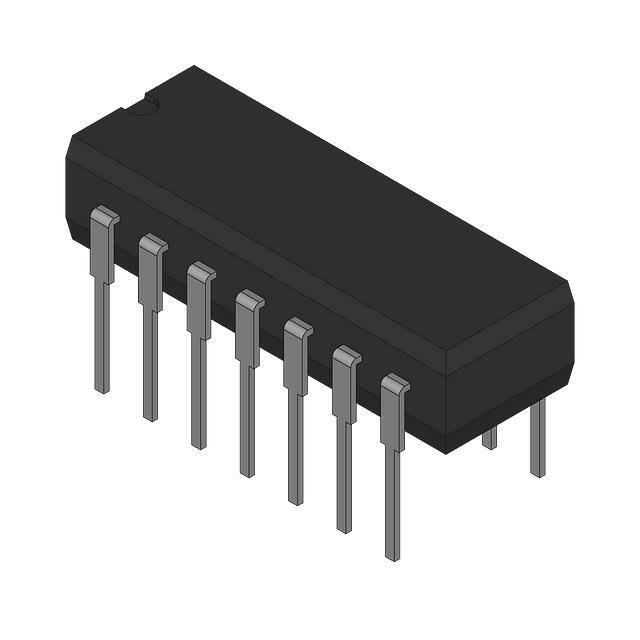
Device Information(1)
PART NUMBER
SN54LS06
PACKAGE
BODY SIZE (NOM)
CDIP (14)
19.50 mm × 6.92 mm
LCCC (20)
8.89 mm × 8.89 mm
SN74LS06D
SOIC (14)
8.65 mm × 3.91 mm
SN74LS06DB
SSOP (14)
5.30 mm × 6.20 mm
2 Applications
SN74LS06N
PDIP (14)
19.30 mm × 6.35 mm
•
•
•
•
•
SN74LS06NS
SOP (14)
5.30 mm × 10.20 mm
Factory Automation
Building Automation
Line Drivers
Electronic Point of Sale
Desktop or Notebook PCs
(1) For all available packages, see the orderable addendum at
the end of the data sheet.
Logic Diagram (Positive Logic)
1
2
1A
1Y
3
4
2A
2Y
5
6
3A
3Y
9
8
4A
4Y
11
10
5A
6A
5Y
13
12
6Y
Pin numbers shown are for the D, DB, J, N, and NS packages.
1
An IMPORTANT NOTICE at the end of this data sheet addresses availability, warranty, changes, use in safety-critical applications,
intellectual property matters and other important disclaimers. PRODUCTION DATA.
�SN54LS06, SN74LS06
SDLS020F – MAY 1990 – REVISED JULY 2016
www.ti.com
Table of Contents
1
2
3
4
5
6
7
8
Features ..................................................................
Applications ...........................................................
Description .............................................................
Revision History.....................................................
Pin Configuration and Functions .........................
Specifications.........................................................
1
1
1
2
3
4
6.1
6.2
6.3
6.4
6.5
6.6
6.7
4
4
4
5
5
5
6
Absolute Maximum Ratings ......................................
ESD Ratings ............................................................
Recommended Operating Conditions.......................
Thermal Information .................................................
Electrical Characteristics...........................................
Switching Characteristics ..........................................
Typical Characteristics .............................................
Parameter Measurement Information .................. 7
Detailed Description .............................................. 8
8.1 Overview .................................................................. 8
8.2 Functional Block Diagram ......................................... 8
8.3 Feature Description .................................................. 8
8.4 Device Functional Modes ......................................... 8
9
Application and Implementation .......................... 9
9.1 Application Information ............................................ 9
9.2 Typical Application ................................................... 9
10 Power Supply Recommendations ..................... 11
11 Layout................................................................... 11
11.1 Layout Guidelines ................................................ 11
11.2 Layout Examples................................................... 11
12 Device and Documentation Support ................. 12
12.1
12.2
12.3
12.4
12.5
12.6
12.7
Documentation Support ........................................
Related Links ........................................................
Receiving Notification of Documentation Updates
Community Resources..........................................
Trademarks ...........................................................
Electrostatic Discharge Caution ............................
Glossary ................................................................
12
12
12
12
12
12
12
13 Mechanical, Packaging, and Orderable
Information ........................................................... 12
4 Revision History
NOTE: Page numbers for previous revisions may differ from page numbers in the current version.
Changes from Revision E (February 2004) to Revision F
Page
•
Added Applications section, Device Information table, ESD Ratings table, Feature Description section, Device
Functional Modes, Application and Implementation section, Power Supply Recommendations section, Layout
section, Device and Documentation Support section, and Mechanical, Packaging, and Orderable Information section ...... 1
•
Added Military Disclaimer to Features list .............................................................................................................................. 1
•
Added Applications. ................................................................................................................................................................ 1
•
Changed values in the Thermal Information table to align with JEDEC standards................................................................ 5
2
Submit Documentation Feedback
Copyright © 1990–2016, Texas Instruments Incorporated
Product Folder Links: SN54LS06 SN74LS06
�SN54LS06, SN74LS06
www.ti.com
SDLS020F – MAY 1990 – REVISED JULY 2016
5 Pin Configuration and Functions
D, DB, J, N, and NS Package
14-Pin SOIC, SSOP, CDIP, PDIP, and SOP
Top View
5
10
5Y
3Y
6
9
4A
GND
7
8
4Y
6A
3A
19
5A
2A
4
18
6Y
NC
5
17
NC
2Y
6
16
5A
NC
7
15
NC
3A
8
14
5Y
3Y
9
Not to scale
13
11
4A
4
VCC
2Y
20
6Y
12
12
4Y
3
NC
2A
1
6A
11
13
NC
2
1A
1Y
2
VCC
10
14
GND
1
1Y
1A
3
FK Package
20-Pin LCCC
Top View
Not to scale
Pin Functions
PIN
I/O
DESCRIPTION
SOIC, SSOP,
CDIP, PDIP, SOP
LCCC
1A
1
2
I
1A Input
1Y
2
3
O
1Y Output
2A
3
4
I
2A Input
2Y
4
6
O
2Y Output
3A
5
8
I
3A Input
3Y
6
9
O
3Y Output
4A
9
13
I
4A Input
4Y
8
12
O
4Y Output
5A
11
16
I
5A Input
5Y
10
14
O
5Y Output
6A
13
19
I
6A Input
6Y
12
18
O
6Y Output
GND
7
10
—
Ground
NC
—
1, 5, 7,
11, 15, 17
—
No internal connection
VCC
14
20
—
Power pin
NAME
Copyright © 1990–2016, Texas Instruments Incorporated
Product Folder Links: SN54LS06 SN74LS06
Submit Documentation Feedback
3
�SN54LS06, SN74LS06
SDLS020F – MAY 1990 – REVISED JULY 2016
www.ti.com
6 Specifications
6.1 Absolute Maximum Ratings
over operating free-air temperature range (unless otherwise noted) (1)
MIN
Supply voltage, VCC
Input voltage, VI
(2)
MAX
UNIT
7
V
7
V
Output voltage, VO (SNx4LS06) (2) (3)
30
V
Absolute maximum junction temperature, TJ
150
°C
150
°C
Storage temperature, Tstg
(1)
(2)
(3)
–65
Stresses beyond those listed under Absolute Maximum Ratings may cause permanent damage to the device. These are stress ratings
only, which do not imply functional operation of the device at these or any other conditions beyond those indicated under Recommended
Operating Conditions. Exposure to absolute-maximum-rated conditions for extended periods may affect device reliability.
All voltage values are with respect to GND.
This is the maximum voltage that must be applied to any output when it is in the off state.
6.2 ESD Ratings
VALUE
V(ESD)
(1)
(2)
Electrostatic discharge
Human-body model (HBM), per ANSI/ESDA/JEDEC JS-001 (1)
±500
Charged-device model (CDM), per JEDEC specification JESD22-C101 (2)
±2000
UNIT
V
JEDEC document JEP155 states that 500-V HBM allows safe manufacturing with a standard ESD control process.
JEDEC document JEP157 states that 250-V CDM allows safe manufacturing with a standard ESD control process. Tested on N
package
6.3 Recommended Operating Conditions
over operating free-air temperature range (unless otherwise noted) (1)
MIN
NOM
MAX
4.5
5
5.5
UNIT
VCC
Supply voltage
VIH
High-level input voltage
VIL
Low-level input voltage
0.8
V
VOH
High-level output voltage (SNx4LS06)
30
V
IOL
Low-level output current
TA
Operating free-air temperature
(1)
4
2
V
V
SN54LS06
30
SN74LS06
40
SN54LS06
–55
125
SN74LS06
0
70
mA
°C
All unused inputs of the device must be held at VCC or GND to ensure proper device operation. See the Implications of Slow or Floating
CMOS Inputs application report.
Submit Documentation Feedback
Copyright © 1990–2016, Texas Instruments Incorporated
Product Folder Links: SN54LS06 SN74LS06
�SN54LS06, SN74LS06
www.ti.com
SDLS020F – MAY 1990 – REVISED JULY 2016
6.4 Thermal Information
SN74LS06
THERMAL METRIC (1)
D (SOIC)
DB (SSOP)
N (PDIP)
NS (SOP)
14 PINS
14 PINS
14 PINS
14 PINS
UNIT
85.8
97.4
50.2
82.8
°C/W
RθJA
Junction-to-ambient thermal resistance
RθJC(top)
Junction-to-case (top) thermal resistance
44
49.8
37.5
40.9
°C/W
RθJB
Junction-to-board thermal resistance
40.3
44.5
30
41.4
°C/W
ψJT
Junction-to-top characterization parameter
11.1
16.5
22.3
12.4
°C/W
ψJB
Junction-to-board characterization parameter
40.1
44
29.9
41.1
°C/W
RθJC(bot)
Junction-to-case (bottom) thermal resistance
—
—
—
—
°C/W
(1)
For more information about traditional and new thermal metrics, see the Semiconductor and IC Package Thermal Metrics application
report.
6.5 Electrical Characteristics
over recommended operating free-air temperature range (unless otherwise noted)
TEST CONDITIONS (1)
PARAMETER
VIK
VCC = MIN, II = –12 mA
IOH
VCC = MIN, VIL = 0.8 V, VOH = 30 V, SNx4LS06
MIN
IOL = 16 mA
TYP (2)
0.25
MAX
UNIT
–1.5
V
0.25
mA
0.4
VOL
VCC = MIN, VIH = 2 V
II
VCC = MAX, VI = 7 V
IIH
VCC = MAX, VI = 2.4 V
20
µA
IIL
VCC = MAX, VI = 0.4 V
–0.2
mA
ICCH
VCC= MAX
18
mA
ICCL
VCC= MAX
60
mA
(1)
(2)
IOL = 30 mA
0.7
IOL = 40 mA, SN74LS06
0.7
1
V
mA
For conditions shown as MIN or MAX, use the appropriate value specified under Recommended Operating Conditions.
All typical values are at VCC = 5 V, and TA = 25°C.
6.6 Switching Characteristics
VCC = 5 V and TA = 25°C (see Figure 2)
PARAMETER
TEST CONDITlONS
MIN
TYP
MAX
tPLH
From A (input) to Y (output), RL= 110 Ω, CL = 15 pF
7
15
tPHL
From A (input) to Y (output), RL= 110 Ω, CL = 15 pF
10
20
Copyright © 1990–2016, Texas Instruments Incorporated
Product Folder Links: SN54LS06 SN74LS06
Submit Documentation Feedback
UNIT
ns
5
�SN54LS06, SN74LS06
SDLS020F – MAY 1990 – REVISED JULY 2016
www.ti.com
6.7 Typical Characteristics
10.5
CL 15 pf
10
9.5
tplh(typ) ns
9
8.5
8
7.5
7
6.5
6
5.5
0
5
10
15
20
25
30
35
40
45
50
55
60
65
70
Temperature ( C )
Figure 1. Propagation Delay vs Temperature
6
Submit Documentation Feedback
Copyright © 1990–2016, Texas Instruments Incorporated
Product Folder Links: SN54LS06 SN74LS06
�SN54LS06, SN74LS06
www.ti.com
SDLS020F – MAY 1990 – REVISED JULY 2016
7 Parameter Measurement Information
VCC
Test
Point
VCC
RL
From Output
Under Test
CL
(see Note A)
CL
(see Note A)
LOAD CIRCUIT
FOR 2-STATE TOTEM-POLE OUTPUTS
High-Level
Pulse
1.3 V
5 kΩ
Test
Point
S2
LOAD CIRCUIT
FOR 3-STATE OUTPUTS
LOAD CIRCUIT
FOR OPEN-COLLECTOR OUTPUTS
3V
Timing
Input
1.3 V
S1
(see Note B)
CL
(see Note A)
RL
(see Note B)
RL
From Output
Under Test
VCC
From Output
Under Test
Test
Point
1.3 V
0V
tw
Low-Level
Pulse
1.3 V
tsu
1.3 V
tPLH
3V
1.3 V
1.3 V
0V
tPZL
tPLZ
tPHL
VOH
1.3 V
1.3 V
Waveform 1
(see Notes C
and D)
VOL
tPZH
tPLH
VOH
1.3 V
1.3 V
VOL
VOLTAGE WAVEFORMS
PROPAGATION DELAY TIMES
≈1.5 V
1.3 V
VOL
tPHL
Out-of-Phase
Output
(see Note D)
1.3 V
0V
Output
Control
(low-level
enabling)
0V
In-Phase
Output
(see Note D)
1.3 V
VOLTAGE WAVEFORMS
SETUP AND HOLD TIMES
3V
1.3 V
3V
Data
Input
1.3 V
VOLTAGE WAVEFORMS
PULSE DURATIONS
Input
th
Waveform 2
(see Notes C
and D)
VOL + 0.5 V
tPHZ
VOH
1.3 V
VOH − 0.5 V
≈1.5 V
VOLTAGE WAVEFORMS
ENABLE AND DISABLE TIMES, 3-STATE OUTPUTS
A.
CL includes probe and jig capacitance.
B.
All diodes are 1N3064 or equivalent.
C.
Waveform 1 is for an output with internal conditions such that the output is low, except when disabled by the output
control. Waveform 2 is for an output with internal conditions such that the output is high, except when disabled by the
output control.
D.
S1 and S2 are closed for tPLH, tPHL, tPHZ, and tPLZ; S1 is open and S2 is closed for tPZH; S1 is closed and S2 is open
for tPZL.
E.
Phase relationships between inputs and outputs have been chosen arbitrarily for these examples.
F.
All input pulses are supplied by generators having the following characteristics: PRR ≤ 1 MHz, ZO ≈ 50 Ω, tr≤ 1.5 ns,
tf≤ 2.6 ns.
G.
The outputs are measured one at a time, with one input transition per measurement.
Figure 2. Load Circuits and Voltage Waveforms
Copyright © 1990–2016, Texas Instruments Incorporated
Product Folder Links: SN54LS06 SN74LS06
Submit Documentation Feedback
7
�SN54LS06, SN74LS06
SDLS020F – MAY 1990 – REVISED JULY 2016
www.ti.com
8 Detailed Description
8.1 Overview
The SNx4LS06 devices are open-collector output inverters. The maximum sink current for the SN54LS06 device
is 30 mA, and for the SN74LS06 device it is 40 mA. These devices are compatible with most TTL families. Inputs
are diode-clamped to minimize transmission effects, which simplifies design. Typical power dissipation is
175 mW, and average propagation delay time is 8 ns.
8.2 Functional Block Diagram
VCC
2.5 kŸ
9 kŸ
1 kŸ
15 kŸ
Output
2.5 kŸ
Input
2 kŸ
2 kŸ
GND
Copyright © 2016, Texas Instruments Incorporated
8.3 Feature Description
The SNx4LS06 devices can convert most TTL voltage circuit voltage level to MOS levels. The devices have high
sink-current capability of up to 40 mA. The open-collector driver can be used for typical applications including
Indicator lamps and relays.
8.4 Device Functional Modes
Table 1 lists the functional modes of the SNx4LS06 devices.
Table 1. Function Table
INPUT
A
8
Submit Documentation Feedback
OUTPUT
Y
H
L
L
Hi-Z
Copyright © 1990–2016, Texas Instruments Incorporated
Product Folder Links: SN54LS06 SN74LS06
�SN54LS06, SN74LS06
www.ti.com
SDLS020F – MAY 1990 – REVISED JULY 2016
9 Application and Implementation
NOTE
Information in the following applications sections is not part of the TI component
specification, and TI does not warrant its accuracy or completeness. TI’s customers are
responsible for determining suitability of components for their purposes. Customers should
validate and test their design implementation to confirm system functionality.
9.1 Application Information
The open-collector device is suitable for high-drive and high-voltage translation applications.
9.2 Typical Application
Vpwr
Vcc
Control signal
1k
Vcc
Input
Vpu 30V
1k
Copyright © 2016, Texas Instruments Incorporated
Figure 3. Application Schematic
9.2.1 Design Requirements
The SNx4LS06 are open-collector devices which can sink current (up to 40 mA on SN74LS06). The devices can
be used in applications such as LED drivers and voltage translation using pullup resistors.
9.2.2 Detailed Design Procedure
1. Recommended input conditions:
– Specified high and low levels. See (VIH and VIL) in the Recommended Operating Conditions.
– Inputs are overvoltage tolerant allowing them to go as high as 5.5 V at any valid VCC.
2. Recommended output conditions:
– Load currents must not exceed (IO max) per output.
– Outputs can be pulled up to 30 V.
Copyright © 1990–2016, Texas Instruments Incorporated
Product Folder Links: SN54LS06 SN74LS06
Submit Documentation Feedback
9
�SN54LS06, SN74LS06
SDLS020F – MAY 1990 – REVISED JULY 2016
www.ti.com
Typical Application (continued)
9.2.3 Application Curve
14
CL 15pF
13.5
13
tplh(typ) ns
12.5
12
11.5
11
10.5
10
9.5
9
8.5
0
5
10
15
20
25
30
35
40
45
50
55
60
65
70
Temperature ( C )
Figure 4. Propagation Delay vs Temperature
10
Submit Documentation Feedback
Copyright © 1990–2016, Texas Instruments Incorporated
Product Folder Links: SN54LS06 SN74LS06
�SN54LS06, SN74LS06
www.ti.com
SDLS020F – MAY 1990 – REVISED JULY 2016
10 Power Supply Recommendations
The power supply can be any voltage between the minimum and maximum supply voltage rating located in the
Recommended Operating Conditions.
Each VCC pin must have a good bypass capacitor to prevent power disturbance. For devices with a single supply,
TI recommends a 0.1-µF capacitor, and if there are multiple VCC pins, then TI recommends a 0.01-µF or 0.022µF capacitor for each power pin. It is ok to parallel multiple bypass capacitors to reject different frequencies of
noise. 0.1-µF and 1-µF capacitors are commonly used in parallel. The bypass capacitor must be installed as
close to the power pin as possible for best results.
11 Layout
11.1 Layout Guidelines
When using multiple bit logic devices, inputs must not ever float. In many cases, functions or parts of functions of
digital logic devices are unused; for example, when only two inputs of a triple-input and gate are used or only 3
of the 4 buffer gates are used. Such input pins must not be left unconnected because the undefined voltages at
the outside connections result in undefined operational states. The following rules must be observed under all
circumstances. All unused inputs of digital logic devices must be connected to a high or low bias to prevent them
from floating. The logic level that must be applied to any particular unused input depends on the function of the
device. Generally they are tied to GND or VCC whichever make more sense or is more convenient. TI
recommends keeping the signal lines as short and as straight as possible (see Figure 6). Incorporation of
microstrip or stripline techniques are also recommended when signal lines are more than 1" long. These traces
must be designed with a characteristic impedance of either 50 Ω or 75 Ω as required by the application.
11.2 Layout Examples
VCC
Input
Unused Input
Output
Unused Input
Output
Input
Figure 5. Layout Schematic
Figure 6. Signal Line Layout
Copyright © 1990–2016, Texas Instruments Incorporated
Product Folder Links: SN54LS06 SN74LS06
Submit Documentation Feedback
11
�SN54LS06, SN74LS06
SDLS020F – MAY 1990 – REVISED JULY 2016
www.ti.com
12 Device and Documentation Support
12.1 Documentation Support
12.1.1 Related Documentation
For related documentation see the following:
Implications of Slow or Floating CMOS Inputs (SCBA004)
12.2 Related Links
The table below lists quick access links. Categories include technical documents, support and community
resources, tools and software, and quick access to sample or buy.
Related Links
PARTS
PRODUCT FOLDER
SAMPLE & BUY
TECHNICAL
DOCUMENTS
TOOLS &
SOFTWARE
SUPPORT &
COMMUNITY
SN54LS06
Click here
Click here
Click here
Click here
Click here
SN74LS06
Click here
Click here
Click here
Click here
Click here
SN74LS16
Click here
Click here
Click here
Click here
Click here
12.3 Receiving Notification of Documentation Updates
To receive notification of documentation updates, navigate to the device product folder on ti.com. In the upper
right corner, click on Alert me to register and receive a weekly digest of any product information that has
changed. For change details, review the revision history included in any revised document.
12.4 Community Resources
The following links connect to TI community resources. Linked contents are provided "AS IS" by the respective
contributors. They do not constitute TI specifications and do not necessarily reflect TI's views; see TI's Terms of
Use.
TI E2E™ Online Community TI's Engineer-to-Engineer (E2E) Community. Created to foster collaboration
among engineers. At e2e.ti.com, you can ask questions, share knowledge, explore ideas and help
solve problems with fellow engineers.
Design Support TI's Design Support Quickly find helpful E2E forums along with design support tools and
contact information for technical support.
12.5 Trademarks
E2E is a trademark of Texas Instruments.
All other trademarks are the property of their respective owners.
12.6 Electrostatic Discharge Caution
These devices have limited built-in ESD protection. The leads should be shorted together or the device placed in conductive foam
during storage or handling to prevent electrostatic damage to the MOS gates.
12.7 Glossary
SLYZ022 — TI Glossary.
This glossary lists and explains terms, acronyms, and definitions.
13 Mechanical, Packaging, and Orderable Information
The following pages include mechanical, packaging, and orderable information. This information is the most
current data available for the designated devices. This data is subject to change without notice and revision of
this document. For browser-based versions of this data sheet, refer to the left-hand navigation.
12
Submit Documentation Feedback
Copyright © 1990–2016, Texas Instruments Incorporated
Product Folder Links: SN54LS06 SN74LS06
�PACKAGE OPTION ADDENDUM
www.ti.com
14-Aug-2021
PACKAGING INFORMATION
Orderable Device
Status
(1)
Package Type Package Pins Package
Drawing
Qty
Eco Plan
(2)
Lead finish/
Ball material
MSL Peak Temp
Op Temp (°C)
Device Marking
(3)
(4/5)
(6)
5962-9861701Q2A
ACTIVE
LCCC
FK
20
1
Non-RoHS
& Green
SNPB
N / A for Pkg Type
-55 to 125
59629861701Q2A
SNJ54LS
06FK
5962-9861701QCA
ACTIVE
CDIP
J
14
1
Non-RoHS
& Green
SNPB
N / A for Pkg Type
-55 to 125
5962-9861701QC
A
SNJ54LS06J
SN54LS06J
ACTIVE
CDIP
J
14
1
Non-RoHS
& Green
SNPB
N / A for Pkg Type
-55 to 125
SN54LS06J
SN74LS06D
ACTIVE
SOIC
D
14
50
RoHS & Green
NIPDAU
Level-1-260C-UNLIM
0 to 70
LS06
SN74LS06DBR
ACTIVE
SSOP
DB
14
2000
RoHS & Green
NIPDAU
Level-1-260C-UNLIM
0 to 70
LS06
SN74LS06DG4
ACTIVE
SOIC
D
14
50
RoHS & Green
NIPDAU
Level-1-260C-UNLIM
0 to 70
LS06
SN74LS06DR
ACTIVE
SOIC
D
14
2500
RoHS & Green
NIPDAU
Level-1-260C-UNLIM
0 to 70
LS06
SN74LS06DRE4
ACTIVE
SOIC
D
14
2500
RoHS & Green
NIPDAU
Level-1-260C-UNLIM
0 to 70
LS06
SN74LS06N
ACTIVE
PDIP
N
14
25
RoHS & Green
NIPDAU
N / A for Pkg Type
0 to 70
SN74LS06N
SN74LS06NE4
ACTIVE
PDIP
N
14
25
RoHS & Green
NIPDAU
N / A for Pkg Type
0 to 70
SN74LS06N
SN74LS06NSR
ACTIVE
SO
NS
14
2000
RoHS & Green
NIPDAU
Level-1-260C-UNLIM
0 to 70
74LS06
SN74LS06NSRG4
ACTIVE
SO
NS
14
2000
RoHS & Green
NIPDAU
Level-1-260C-UNLIM
0 to 70
74LS06
SNJ54LS06FK
ACTIVE
LCCC
FK
20
1
Non-RoHS
& Green
SNPB
N / A for Pkg Type
-55 to 125
59629861701Q2A
SNJ54LS
06FK
SNJ54LS06J
ACTIVE
CDIP
J
14
1
Non-RoHS
& Green
SNPB
N / A for Pkg Type
-55 to 125
5962-9861701QC
A
SNJ54LS06J
(1)
The marketing status values are defined as follows:
ACTIVE: Product device recommended for new designs.
LIFEBUY: TI has announced that the device will be discontinued, and a lifetime-buy period is in effect.
Addendum-Page 1
Samples
�PACKAGE OPTION ADDENDUM
www.ti.com
14-Aug-2021
NRND: Not recommended for new designs. Device is in production to support existing customers, but TI does not recommend using this part in a new design.
PREVIEW: Device has been announced but is not in production. Samples may or may not be available.
OBSOLETE: TI has discontinued the production of the device.
(2)
RoHS: TI defines "RoHS" to mean semiconductor products that are compliant with the current EU RoHS requirements for all 10 RoHS substances, including the requirement that RoHS substance
do not exceed 0.1% by weight in homogeneous materials. Where designed to be soldered at high temperatures, "RoHS" products are suitable for use in specified lead-free processes. TI may
reference these types of products as "Pb-Free".
RoHS Exempt: TI defines "RoHS Exempt" to mean products that contain lead but are compliant with EU RoHS pursuant to a specific EU RoHS exemption.
Green: TI defines "Green" to mean the content of Chlorine (Cl) and Bromine (Br) based flame retardants meet JS709B low halogen requirements of


 工商网监
湘ICP备2023018690号
工商网监
湘ICP备2023018690号
