TAS5102
TAS5103
www.ti.com .............................................................................................................................................................. SLLS801A – JUNE 2008 – REVISED JUNE 2008
20-W/15-W STEREO DIGITAL AMPLIFIER POWER STAGE
FEATURES
1
• 2×20 W at 10% THD+N Into 8-Ω BTL at 18 V
(With Heatsink for TAS5102)
• 2×15 W at 10% THD+N Into 8-Ω BTL at 15.5 V
for TAS5103
• 2×10 W at 10% THD+N Into 8-Ω BTL at 13 V
• >100-dB SNR (A-Weighted)
• 90%) With
180-mΩ Output MOSFETs
• Wide PVDD Range from 8V to 23V
• Power-On Reset for Protection on Power Up
Without Any Power-Supply Sequencing
• Integrated Self-Protection Circuits Including
Undervoltage, Overtemperature, Overcurrent,
Short Circuit
• Built-In Regulator for Gate Drive Supply
• Error Reporting
• EMI Compliant When Used With
Recommended System Design
2
A low-cost, high-fidelity audio system can be built
using a TI chipset, comprising a modulator (e.g.,
TAS5086) and the TAS5102/TAS5103. This system
only requires a simple passive LC demodulation filter
to deliver high-quality,
high-efficiency
audio
amplification with proven EMI compliance. These
devices require two power supplies, at 3.3 V for
VREG, and up to 23 V for PVDD. The
TAS5102/TAS5103 does not require power-up
sequencing due to internal power-on reset. The
efficiency of this digital amplifier is greater than 90%
into 8 Ω, which enables the use of smaller power
supplies and heatsinks.
The TAS5102/3 has an innovative protection system
integrated on chip, safeguarding the device against a
wide range of fault conditions that could damage the
system. These safeguards are short-circuit protection,
overcurrent protection, undervoltage protection, and
overtemperature protection. The TAS5102/TAS5103
has a new proprietary current-limiting circuit that
reduces the possibility of device shutdown during
high-level music transients.
BTL OUTPUT POWER
vs
SUPPLY VOLTAGE
35
f = 1 kHz
RL = 8 Ω (BTL)
Gain = 3 dB
30
•
•
•
•
Televisions
Mini/Micro Audio Systems
DVD Receivers
Home Theaters
DESCRIPTION
The TAS5102/TAS5103 are integrated stereo digital
amplifier power stages with an advanced protection
system. The TAS5102/TAS5103 are capable of
driving an 8-Ω bridge-tied load (BTL) at up to 20
W/15 W per channel with low integrated noise at the
output, low THD+N performance, and low idle power
dissipation.
PO − Output Power − W
APPLICATIONS
25
THD+N = 10%
20
15
THD+N = 1%
10
5
0
5
10
15
20
VCC − Supply Voltage − V
25
G009
1
2
Please be aware that an important notice concerning availability, standard warranty, and use in critical applications of Texas
Instruments semiconductor products and disclaimers thereto appears at the end of this data sheet.
PowerPAD is a trademark of Texas Instruments.
PRODUCTION DATA information is current as of publication date.
Products conform to specifications per the terms of the Texas
Instruments standard warranty. Production processing does not
necessarily include testing of all parameters.
Copyright © 2008, Texas Instruments Incorporated
�TAS5102
TAS5103
SLLS801A – JUNE 2008 – REVISED JUNE 2008 .............................................................................................................................................................. www.ti.com
These devices have limited built-in ESD protection. The leads should be shorted together or the device placed in conductive foam
during storage or handling to prevent electrostatic damage to the MOS gates.
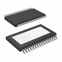
DEVICE INFORMATION
Pin Assignment
The TAS5102/TAS5103 are available in a thermally enhanced package:
• TAS5102 Pad Up 32-pin HTSSOP PowerPAD™ package (DAD)
• TAS5103 Pad Down 32-pin HTSSOP PowerPAD™ package (DAP)
DAD PACKAGE
(TOP VIEW)
DAP PACKAGE
(TOP VIEW)
GVDD_AB
VREG
AGND
GND
SSTIMER
BST_A
PVDD_A
OUT_A
PGND_AB
PGND_AB
OTW
RESET
PWM_A
PWM_B
PWM_C
PWM_D
FAULT
OC_ADJ
M1
M2
GVDD_CD
OUT_B
PVDD_B
BST_B
BST_C
PVDD_C
OUT_C
PGND_CD
PGND_CD
OUT_D
PVDD_D
BST_D
GVDD_CD
M2
M1
OC_ADJ
FAULT
PWM_D
PWM_C
PWM_B
PWM_A
RESET
OTW
SSTIMER
GND
AGND
VREG
GVDD_AB
BST_D
PVDD_D
OUT_D
PGND_CD
PGND_CD
OUT_C
PVDD_C
BST_C
BST_B
PVDD_B
OUT_B
PGND_AB
PGND_AB
OUT_A
PVDD_A
BST_A
MODE Selection Pins
Mode
M2
M1
0
0
0
(1)
(2)
1
1
0
1
1
PWM INPUT
2N
(1)
1N
1N
OUTPUT CONFIGURATION
AD/BD modulation
(1)
(1)
PROTECTION SCHEME
2 channels BTL output
AD modulation
2 channels BTL output
AD modulation
4 channels SE output
BTL mode
(2)
BTL mode
(2)
Protection works similarly to BTL mode (2). Only
difference in SE mode is that OUT_X is Hi-Z instead
of a pulldown through internal pulldown resistor.
Reserved
The 1N and 2N naming convention is used to indicate the required number of PWM lines to the power stage per channel in a specific
mode.
An overcurrent protection (OC) occurring on A or B causes all channels to shut down. An OC on C or D works similarly. Global errors
like overtemperature error (OTE), undervoltage protection (UVP), and power-on reset (POR) affect all channels.
Package Heat Dissipation Ratings
PARAMETER
RθJC (°C/W)
RθJA (°C/W)
(1)
2
TAS5102DAD
TAS5103DAP
1.69
1.69
See Note
(1)
23.5
The TAS5102 package is thermally enhanced for conductive cooling using an exposed metal pad area. It is impractical to use the device
with the pad exposed to ambient air as the only means for heat dissipation for higher power applications.
For this reason, RθJA, a system parameter that characterizes the thermal treatment, is provided in the Application Information section of
the data sheet. An example and discussion of typical system RθJA values are provided in the Thermal Information section. This example
provides additional information regarding the power dissipation ratings. This example should be used as a reference to calculate the
heat dissipation ratings for a specific application. TI application engineering provides technical support to design heatsinks if needed.
Also, for additional general information on PowerPad packages, see TI document SLMA002B.
Submit Documentation Feedback
Copyright © 2008, Texas Instruments Incorporated
Product Folder Link(s): TAS5102 TAS5103
�TAS5102
TAS5103
www.ti.com .............................................................................................................................................................. SLLS801A – JUNE 2008 – REVISED JUNE 2008
ABSOLUTE MAXIMUM RATINGS (1)
over operating free-air temperature range (unless otherwise noted)
UNIT
PVDD_X to GND_X DC
-0.3 to 23
V
–0.3 to 32
V
OUT_X to GND_X
(2)
–0.3 to 32
V
BST_X to GND_X
(2)
–0.3 to 43.2
V
VREG to AGND
–0.3 to 4.2
V
GVDD to GND
-0.3 to 13.2
V
GND_X to GND
–0.3 to 0.3
V
GND_X to AGND
–0.3 to 0.3
V
GND to AGND
–0.3 to 0.3
V
PWM_X, OC_ADJ, M1, M2 to AGND
–0.3 to 4.2
V
RESET_X, FAULT, OTW to AGND
–0.3 V to 7
V
9
mA
PVDD_X to GND_X
(2)
Maximum continuous sink current (FAULT, OTW)
TJ
TSTG
Maximum operating junction temperature range,
Storage temperature range
Minimum pulse duration, low
(1)
(2)
0 to 150
°C
–65 to 150
°C
50
ns
Stresses beyond those listed under "absolute maximum ratings" may cause permanent damage to the device. These are stress ratings
only, and functional operation of the device at these or any other conditions beyond those indicated under "recommended operating
conditions" is not implied. Exposure to absolute-maximum-rated conditions for extended periods may affect device reliability.
These voltages represent the dc voltage + peak ac waveform measured at the terminal of the device in all conditions.
ORDERING INFORMATION
TA
0°C to 70°C
(1)
PACKAGE (1)
DESCRIPTION
TAS5102DAD
32-pin HTSSOP
TAS5103DAP
32-pin HTSSOP
For the most current package and ordering information, see the Package Option Addendum at the end of this document, or see the TI
website at www.ti.com.
Submit Documentation Feedback
Copyright © 2008, Texas Instruments Incorporated
Product Folder Link(s): TAS5102 TAS5103
3
�TAS5102
TAS5103
SLLS801A – JUNE 2008 – REVISED JUNE 2008 .............................................................................................................................................................. www.ti.com
Pin Functions
PIN
NAME
(1)
4
TAS5102
NO.
TAS5103
NO
FUNCTION
(1)
DESCRIPTION
AGND
3
14
P
Analog ground
BST_A
32
17
P
HS bootstrap supply (BST). External capacitor to OUT_A required.
BST_B
25
24
P
HS bootstrap supply (BST). External capacitor to OUT_B required.
BST_C
24
25
P
HS bootstrap supply (BST). External capacitor to OUT_C required.
BST_D
17
32
P
HS bootstrap supply (BST). External capacitor to OUT_D required.
FAULT
12
5
O
Device error signal (shutdown); open drain
GND
4
13
P
Ground
PGND_AB
29
20
P
Power ground for half-bridges A and B
PGND_AB
28
21
P
Power ground for half-bridges A and B
PGND_CD
21
28
P
Power ground for half-bridges C and D
PGND_CD
20
29
P
Power ground for half-bridge D
GVDD_AB
1
16
P
Gate-drive voltage supply. Requires 1-µF capacitor to GND.
GVDD_CD
16
1
P
Gate-drive voltage supply. Requires 1-µF capacitor to GND.
M2
15
2
I
Mode selection 2, connect to either AGND or VREG, no pull-up or pull-down
resistors
M1
14
3
I
Mode selection 1, connect to either AGND or VREG, no pull-up or pull-down
resistors
OC_ADJ
13
4
O
Analog overcurrent programming. Requires resistor to ground.
OTW
6
11
O
Overtemperature warning signal, push-pull, active high
OUT_A
30
19
O
Output, half-bridge A
OUT_B
27
22
O
Output, half-bridge B
OUT_C
22
27
O
Output, half-bridge C
OUT_D
19
30
O
Output, half-bridge D
PVDD_A
31
18
P
Power supply input for half-bridge A. Requires close decoupling of 0.1-µF
capacitor to GND_A.
PVDD_B
26
23
P
Power supply input for half-bridge B. Requires close decoupling of 0.1-µF
capacitor to GND_B.
PVDD_C
23
26
P
Power supply input for half-bridge C. Requires close decoupling of 0.1-µF
capacitor to GND_C.
PVDD_D
18
31
P
Power supply input for half-bridge D. Requires close decoupling of 0.1-µF
capacitor to GND_D.
PWM_A
8
9
I
Input signal for half-bridge A
PWM_B
9
8
I
Input signal for half-bridge B
PWM_C
10
7
I
Input signal for half-bridge C
PWM_D
11
6
I
Input signal for half-bridge D
RESET
7
10
I
PWM is not active if RESET goes low.
SSTIMER
5
12
I
Controls start/stop time of PWM modulation. Requires 2.2 nF capacitor to GND
for AD BTL. Leave pin floating (NC) for BD BTL mode. Also, leave pin floating
(NC) for SE mode.
VREG
2
15
P
Digital regulator supply filter. Requires 0.1-µF capacitor to AGND.
I = input, O = output, P = power
Submit Documentation Feedback
Copyright © 2008, Texas Instruments Incorporated
Product Folder Link(s): TAS5102 TAS5103
�TAS5102
TAS5103
www.ti.com .............................................................................................................................................................. SLLS801A – JUNE 2008 – REVISED JUNE 2008
SYSTEM BLOCK DIAGRAM
OTW
System
Microcontroller
FAULT
TAS5508
OTW
FAULT
BST_A
BST_B
RESET
VALID
PWM_A
LeftChannel
Output
OUT_A
Output
H-Bridge 1
Input
H-Bridge 1
PWM_B
OUT_B
Bootstrap
Capacitors
2nd-Order L-C
Output Filter
for Each
Half-Bridge
2-Channel
H-Bridge
BTL Mode
OUT_C
PWM_C
2
8 V - 23 V
PVDD
System
Power
Supply
GND
3.3 V
4
PVDD
GVDD
Power
Supply
Decoupling
OUT_D
2nd-Order L-C
Output Filter
for Each
Half-Bridge
OC_ADJ
AGND
VREG
BST_C
GND
M2
GND_A, B, C, D
M1
GVDD_AB, CD
Hardwire
Mode
Control
Output
H-Bridge 2
Input
H-Bridge 2
PWM_D
PVDD_A, B, C, D
RightChannel
Output
BST_D
Bootstrap
Capacitors
4
VREG
Power Supply
Decoupling
Hardwire
OC Limit
GND
VREG
VAC
Submit Documentation Feedback
Copyright © 2008, Texas Instruments Incorporated
Product Folder Link(s): TAS5102 TAS5103
5
�TAS5102
TAS5103
SLLS801A – JUNE 2008 – REVISED JUNE 2008 .............................................................................................................................................................. www.ti.com
FUNCTIONAL BLOCK DIAGRAM
Undervoltage
Protection
OTW
Internal Pullup
Resistors to VREG
Power
On
Reset
Protection
and
I/O Logic
M2
4
VREG
FAULT
M1
4
AGND
Temp.
Sense
GND
VALID
Overload
Protection
Isense
OC_ADJ
BST_D
PVDD_D
PWM_D
PWM
Rcv.
Ctrl.
Timing
Gate
Drive
OUT_D
BTL/PBTL−Configuration
Pulldown Resistor
GND_D
GVDD_CD
Regulator
GVDD_CD
BST_C
PVDD_C
PWM_C
PWM
Rcv
.
Ctrl.
Timing
Gate
Drive
OUT_C
BTL/PBTL−Configuration
Pulldown Resistor
GND_C
BST_B
PVDD_B
PWM_B
PWM
Rcv
.
Ctrl.
Timing
Gate
Drive
OUT_B
BTL/PBTL−Configuration
Pulldown Resistor
GVDD_AB
Regulator
GND_B
GVDD_AB
BST_A
PVDD_A
PWM_A
PWM
Rcv
.
Ctrl.
Timing
Gate
Drive
OUT_A
BTL/PBTL−Configuration
Pulldown Resistor
GND_A
6
Submit Documentation Feedback
Copyright © 2008, Texas Instruments Incorporated
Product Folder Link(s): TAS5102 TAS5103
�TAS5102
TAS5103
www.ti.com .............................................................................................................................................................. SLLS801A – JUNE 2008 – REVISED JUNE 2008
RECOMMENDED OPERATING CONDITIONS
MIN
VSS
UNIT
DC supply voltage
8
18
23
V
Supply for Protection and I/O Logic, VREG
DC supply voltage
3
3.3
3.6
V
6-8
Output filter: L = 10 µH, C = 470 nF.
Output AD modulation, switching
frequency > 350 kHz
Load impedance
RL (PBTL)
Ω
3-4
3-4
LO (BTL)
LO (SE)
MAX
Half-bridge supply, PVDD_X
RL (BTL)
RL (SE)
TYP
200
Minimum output inductance under
short-circuit condition
Output-filter inductance
200
LO (PBTL)
nH
200
FPWM
PWM frame rate
TJ
Junction temperature
192
384
0
432
kHz
125
°C
AC Characteristics (BTL)
PVDD_X = 18 V, BTL mode, RL = 8 Ω, ROC = 22 KΩ, CBST = 33-nF, audio frequency = 1 kHz, AES17 filter,
FPWM = 384 kHz, ambient temperature = 25°C (unless otherwise noted). Audio performance is recorded as a chipset, using
TAS5086 PWM processor with an effective modulation index limit of 96.1%. All performance is in accordance with
recommended operating conditions, unless otherwise specified.
PARAMETER
PO
Power output per channel
TEST CONDITIONS
MIN
20
PVDD = 18 V, 7% THD
18
PVDD = 12 V, 10% THD
9
PVDD = 12 V, 7% THD
0.15
PVDD = 12V, Po =4.5 W (half-power)
0.18
1W
0.05
Total harmonic distortion + noise
Vn
Output integrated noise
A-weighted
SNR
Signal-to-noise ratio
(1)
A-weighted
DNR
Dynamic range
(1)
(2)
A-weighted, input level = –60 dBFS using
TAS5086 modulator
Power dissipation due to idle losses (IPVDD_X) PO = 0 W, 4 channels switching
MAX
UNIT
W
8
PVDD = 18V, Po =10 W (half-power)
THD+N
PD
TYP
PVDD = 18 V, 10% THD
(2)
%
50
µV
94
105
dB
94
105
dB
0.6
W
SNR is calculated relative to 0-dBFS input level.
Actual system idle losses are affected by core losses of output inductors.
Submit Documentation Feedback
Copyright © 2008, Texas Instruments Incorporated
Product Folder Link(s): TAS5102 TAS5103
7
�TAS5102
TAS5103
SLLS801A – JUNE 2008 – REVISED JUNE 2008 .............................................................................................................................................................. www.ti.com
AC Characteristics (Single-Ended Output)
PVDD_X = 18 V, SE mode, RL = 4 Ω, ROC = 22 kΩ, CBST = 33-nF, audio frequency = 1 kHz, AES17 filter, FPWM = 384 kHz,
ambient temperature = 25°C (unless otherwise noted). Audio performance is recorded as a chipset, using TAS5086 PWM
processor with an effective modulation index limit of 96.1%. All performance is in accordance with recommended operating
conditions, unless otherwise specified.
PARAMETER
TEST CONDITIONS
MIN
PVDD = 18 V, 10% THD
PO
Power output per channel
TYP MAX
UNIT
10
PVDD = 18 V, 7% THD
9
PVDD = 12 V, 10% THD
4.5
PVDD = 12 V, 7% THD
W
4
PVDD = 18V, Po =5 W (half-power)
0.2
PVDD = 12V, Po =2.25 W (half-power)
0.2
THD+
N
Total harmonic distortion + noise
Vn
Output integrated noise
A-weighted
50
µV
SNR
Signal-to-noise ratio (1)
A-weighted
105
dB
DNR
Dynamic range
A-weighted, input level = –60 dBFS using TAS5086 modulator
105
dB
PD
Power dissipation due to idle
losses (IPVDD_X)
0.6
W
(1)
(2)
8
PO = 0 W, 4 channels switching
(2)
%
SNR is calculated relative to 0-dBFS input level.
Actual system idle losses are affected by core losses of output inductors.
Submit Documentation Feedback
Copyright © 2008, Texas Instruments Incorporated
Product Folder Link(s): TAS5102 TAS5103
�TAS5102
TAS5103
www.ti.com .............................................................................................................................................................. SLLS801A – JUNE 2008 – REVISED JUNE 2008
DC Characteristics
RL= 8 Ω, FPWM = 384 kHz (unless otherwise noted). All performance is in accordance with recommended operating
conditions, unless otherwise specified.
PARAMETER
TEST CONDITIONS
MIN
TYP MAX
UNIT
Internal Voltage Regulator and Current Consumption
VSS
Digital Input Supply Voltage, VREG
I(VREG)
Supply current, VREG
I(PVDD_X)
Total Half-bridge idle current
3.3
3.6
Operating, 50% duty cycle
3
6.5
10
Reset mode, no switching
6.5
10
50% duty cycle, without output filter or load
35
50
5
6.3
Reset mode, no switching
V
mA
mA
Output Stage MOSFETs
RDS(on)
Drain-to-source resistance, LS
TJ = 25°C, includes metallization resistance
180
mΩ
Drain-to-source resistance, HS
TJ = 25°C, includes metallization resistance
180
mΩ
I/O Protection
Vuvp,G
Undervoltage protection limit, GVDD_X,
voltage rising
5.7
V
Vuvp,G
Undervoltage protection limit, GVDD_X,
voltage falling
5.5
V
Overtemperature warning
125
°C
25
°C
OTW
(1)
OTWHYST (1)
Temperature drop needed below OTW
temperature for OTW to be inactive after
the OTW event
OTE (1)
Overtemperature error
150
°C
OTE-OTW (1)
OTE-OTW differential
25
°C
OTEHYST (1)
A RESET must occur to exit shutdown
and to release FAULT following an OTE
event.
30
°C
OCPC
Overcurrent protection counter
FPWM = 384 kHz
0.63
ms
IOC
Overcurrent limit protection
Resistor—programmable, max. current,
ROCP = 22 kΩ
4.5
A
IOCT
Overcurrent response time
150
ns
ROCP
OC programming resistor range
RPD
Internal pulldown resistor at the output of Connected when RESET is active to provide
each half-bridge
bootstrap capacitor charge. Not used in SE mode
(1)
Resistor tolerance = 5% for typical value; the
minimum resistance should not be less than 20kΩ.
20
22
24
3
kΩ
kΩ
Specified by design
Submit Documentation Feedback
Copyright © 2008, Texas Instruments Incorporated
Product Folder Link(s): TAS5102 TAS5103
9
�TAS5102
TAS5103
SLLS801A – JUNE 2008 – REVISED JUNE 2008 .............................................................................................................................................................. www.ti.com
DC Characteristics (continued)
RL= 8 Ω, FPWM = 384 kHz (unless otherwise noted). All performance is in accordance with recommended operating
conditions, unless otherwise specified.
PARAMETER
TEST CONDITIONS
MIN
TYP MAX
UNIT
Static Digital Specifications
VIH
High-level input voltage
VIL
Low-level input voltage
Ilkg
2
PWM_A, PWM_B, PWM_C, PWM_D, M1, M2,
RESET
V
0.8
Static, High PWM_A, PWM_B, PWM_C, PWM_D,
M1, M2, RESET
Input leakage current
V
100
µA
Static, Low PWM_A, PWM_B, PWM_C, PWM_D,
M1, M2, RESET
–10
10
FAULT
RINT_PU
Internal pullup resistance, FAULT
VOH
High-level output voltage
VOL
Low-level output voltage
Internal pullup resistor
20
26
32
3
3.3
3.6
External pullup of 4.7 kΩ to 5 V
5.5
IO = 4 mA
0.25
0.5
kΩ
V
V
TYPICAL CHARACTERISTICS
TOTAL HARMONIC DISTORTION + NOISE
vs
FREQUENCY
TOTAL HARMONIC DISTORTION + NOISE
vs
FREQUENCY
10
VCC = 8 V
RL = 8 Ω (BTL)
Gain = 3 dB
THD+N − Total Harmonic Distortion + Noise − %
THD+N − Total Harmonic Distortion + Noise − %
10
1
PO = 2.5 W
PO = 0.5 W
0.1
PO = 1 W
0.01
0.001
20
100
1k
10k 20k
VCC = 12 V
RL = 8 Ω (BTL)
Gain = 3 dB
1
PO = 5 W
0.1
0.01
0.001
20
f − Frequency − Hz
PO = 2.5 W
100
PO = 0.5 W
1k
G001
Figure 1.
10
10k 20k
f − Frequency − Hz
G002
Figure 2.
Submit Documentation Feedback
Copyright © 2008, Texas Instruments Incorporated
Product Folder Link(s): TAS5102 TAS5103
�TAS5102
TAS5103
www.ti.com .............................................................................................................................................................. SLLS801A – JUNE 2008 – REVISED JUNE 2008
TYPICAL CHARACTERISTICS (continued)
TOTAL HARMONIC DISTORTION + NOISE
vs
FREQUENCY
TOTAL HARMONIC DISTORTION + NOISE
vs
OUTPUT POWER
10
VCC = 18 V
RL = 8 Ω (BTL)
Gain = 3 dB
THD+N − Total Harmonic Distortion + Noise − %
THD+N − Total Harmonic Distortion + Noise − %
10
1
PO = 10 W
0.1
0.01
0.001
20
PO = 5 W
PO = 1 W
100
1k
VCC = 8 V
RL = 8 Ω (BTL)
Gain = 3 dB
1
f = 20 Hz
0.1
0.01
f = 1 kHz
f = 10 kHz
0.001
0.01
10k 20k
0.1
f − Frequency − Hz
G003
40
G004
Figure 4.
TOTAL HARMONIC DISTORTION + NOISE
vs
OUTPUT POWER
TOTAL HARMONIC DISTORTION + NOISE
vs
OUTPUT POWER
10
VCC = 12 V
RL = 8 Ω (BTL)
Gain = 3 dB
THD+N − Total Harmonic Distortion + Noise − %
THD+N − Total Harmonic Distortion + Noise − %
10
Figure 3.
10
1
f = 20 Hz
0.1
0.01
f = 1 kHz
f = 10 kHz
0.001
0.01
1
PO − Output Power − W
0.1
1
10
PO − Output Power − W
40
VCC = 18 V
RL = 8 Ω (BTL)
Gain = 3 dB
1
f = 20 Hz
0.1
0.01
f = 1 kHz
f = 10 kHz
0.001
0.01
G005
Figure 5.
0.1
1
10
PO − Output Power − W
40
G006
Figure 6.
Submit Documentation Feedback
Copyright © 2008, Texas Instruments Incorporated
Product Folder Link(s): TAS5102 TAS5103
11
�TAS5102
TAS5103
SLLS801A – JUNE 2008 – REVISED JUNE 2008 .............................................................................................................................................................. www.ti.com
TYPICAL CHARACTERISTICS (continued)
EFFICIENCY
vs
OUTPUT POWER
SUPPLY CURRENT
vs
TOTAL OUTPUT POWER
3.0
100
f = 1 kHz
RL = 8 Ω (BTL)
Gain = 3 dB
90
2.5
80
VCC = 12 V
Efficiency − %
ICC − Supply Current − A
VCC = 18 V
70
VCC = 8 V
60
50
40
30
20
VCC = 18 V
1.0
VCC = 12 V
VCC = 8 V
0.0
0
0
5
10
15
20
0
25
5
10
15
20
25
30
35
40
45
PO − Total Output Power − W
PO − Output Power − W
Figure 8.
OUTPUT POWER
vs
SUPPLY VOLTAGE
CROSSTALK
vs
FREQUENCY
50
G008
G007
Figure 7.
35
−20
f = 1 kHz
RL = 8 Ω (BTL)
Gain = 3 dB
30
−30
VCC = 18 V
RL = 8 Ω (BTL)
PO = 0.25 W
Gain = 3 dB
−40
25
Crosstalk − dB
PO − Output Power − W
1.5
0.5
f = 1 kHz
RL = 8 Ω (BTL)
Gain = 3 dB
10
2.0
THD+N = 10%
20
15
THD+N = 1%
Left to Right
−50
Right to Left
−60
−70
10
−80
5
−90
0
5
10
15
20
VCC − Supply Voltage − V
25
−100
20
1k
10k 20k
f − Frequency − Hz
G009
Figure 9.
12
100
G010
Figure 10.
Submit Documentation Feedback
Copyright © 2008, Texas Instruments Incorporated
Product Folder Link(s): TAS5102 TAS5103
�TAS5102
TAS5103
www.ti.com .............................................................................................................................................................. SLLS801A – JUNE 2008 – REVISED JUNE 2008
TYPICAL CHARACTERISTICS (continued)
TOTAL HARMONIC DISTORTION + NOISE
vs
FREQUENCY
TOTAL HARMONIC DISTORTION + NOISE
vs
FREQUENCY
10
VCC = 12 V
RL = 4 Ω (SE)
Gain = 3 dB
THD+N − Total Harmonic Distortion + Noise − %
THD+N − Total Harmonic Distortion + Noise − %
10
1
PO = 2.5 W
0.1
PO = 1 W
PO = 0.5 W
0.01
0.001
20
100
1k
VCC = 18 V
RL = 4 Ω (SE)
Gain = 3 dB
1
PO = 5 W
0.1
PO = 2.5 W
PO = 0.5 W
0.01
0.001
20
10k 20k
100
1k
f − Frequency − Hz
10k 20k
f − Frequency − Hz
G011
G012
Figure 11.
Figure 12.
TOTAL HARMONIC DISTORTION + NOISE
vs
OUTPUT POWER
OUTPUT POWER
vs
SUPPLY VOLTAGE
18
f = 1 kHz
RL = 4 Ω (SE)
Gain = 3 dB
f = 1 kHz
RL = 4 Ω (SE)
Gain = 3 dB
15
1
PO − Output Power − W
THD+N − Total Harmonic Distortion + Noise − %
10
0.1
VCC = 18 V
VCC = 12 V
12
THD+N = 10%
9
6
THD+N = 1%
0.01
3
0.001
0.01
0
0.1
1
10
PO − Output Power − W
40
5
10
15
20
VCC − Supply Voltage − V
G013
Figure 13.
25
G014
Figure 14.
Submit Documentation Feedback
Copyright © 2008, Texas Instruments Incorporated
Product Folder Link(s): TAS5102 TAS5103
13
�TAS5102
TAS5103
SLLS801A – JUNE 2008 – REVISED JUNE 2008 .............................................................................................................................................................. www.ti.com
TYPICAL CHARACTERISTICS (continued)
SUPPLY CURRENT
vs
TOTAL OUTPUT POWER
A-WEIGHTED NOISE
vs
SUPPLY VOLTAGE
0.0
3.0
−20.0
A-Weighted Noise − dBv
ICC − Supply Current − A
2.5
f = 1 kHz
RL = 4 Ω (SE)
Gain = 3 dB
f = 1 kHz
RL = 4 Ω (SE)
Gain = 3 dB
2.0
1.5
VCC = 18 V
1.0
VCC = 12 V
0.5
0.0
0.0
−40.0
−60.0
−80.0
VCC = 8 V
−100.0
5.0
5.0 10.0 15.0 20.0 25.0 30.0 35.0 40.0 45.0
PO − Total Output Power − W
10.0
15.0
20.0
VCC − Supply Voltage − V
G015
Figure 15.
25.0
G016
Figure 16.
CROSSTALK
vs
FREQUENCY
0
−10
Crosstalk − dB
−20
RL = 4 Ω (SE)
PO = 0.25 W
Gain = 3 dB
VCC = 18 V
−30
Left to Right
−40
−50
Right to Left
−60
−70
−80
20
100
1k
10k 20k
f − Frequency − Hz
G018
Figure 17.
14
Submit Documentation Feedback
Copyright © 2008, Texas Instruments Incorporated
Product Folder Link(s): TAS5102 TAS5103
�TAS5102
TAS5103
www.ti.com .............................................................................................................................................................. SLLS801A – JUNE 2008 – REVISED JUNE 2008
TAS5102
0.1uF
16V
0.033uF
50V
1uF
50V
0.1uF
50V
10nF
50V
10
3.3
10uH
0.1uF
16V
0.47uF
50V
10nF
50V
3.3
0.47uF
50V
10uH
*2200pF
50V
0.033uF
50V
0.1uF
50V
1uF
50V
0.1uF
50V
1uF
50V
*AD mode only.
Leave open for BD
mode and SE.
0.033uF
50V
220uF
35V
220uF
35V
330uF
35V
10uH
0.47uF
50V
22k
3.3
10nF
50V
0.47uF
50V
10uH
3.3
0.033uF
50V
1uF
16V
0.1uF
50V
1uF
50V
10nF
50V
2N-BTL
Figure 18. Typical Differential (2N) BTL Application With AD Modulation Filters
Submit Documentation Feedback
Copyright © 2008, Texas Instruments Incorporated
Product Folder Link(s): TAS5102 TAS5103
15
�TAS5102
TAS5103
SLLS801A – JUNE 2008 – REVISED JUNE 2008 .............................................................................................................................................................. www.ti.com
TAS5102
0.1uF
16V
0.033uF
50V
1uF
50V
0.1uF
50V
10nF
50V
10
3.3
10uH
0.1uF
16V
0.47uF
50V
10nF
50V
3.3
0.47uF
50V
10uH
*2200pF
50V
0.033uF
50V
0.1uF
50V
1uF
50V
0.1uF
50V
1uF
50V
*AD mode only.
Leave open for BD
mode and SE.
0.033uF
50V
220uF
35V
220uF
35V
330uF
35V
10uH
0.47uF
50V
22k
3.3
10nF
50V
0.47uF
50V
10uH
3.3
0.033uF
50V
1uF
16V
0.1uF
50V
1uF
50V
10nF
50V
1N-BTL
Figure 19. Typical Non-Differential (1N) BTL Application With AD Modulation Filters
16
Submit Documentation Feedback
Copyright © 2008, Texas Instruments Incorporated
Product Folder Link(s): TAS5102 TAS5103
�TAS5102
TAS5103
www.ti.com .............................................................................................................................................................. SLLS801A – JUNE 2008 – REVISED JUNE 2008
THEORY OF OPERATION
POWER SUPPLIES
To facilitate system design, the TAS5102/3 needs
only a 3.3-V supply in addition to the (typical) 18-V
power-stage supply. An internal voltage regulator
provides suitable voltage levels for the gate drive
circuitry. Additionally, all circuitry requiring a floating
voltage supply, e.g., the high-side gate drive, is
accommodated by built-in bootstrap circuitry requiring
only a few external capacitors.
In order to provide outstanding electrical and
acoustical characteristics, the PWM signal path for
the output stage is designed as identical,
independent half-bridges. For this reason, each
half-bridge has separate bootstrap pins (BST_X), and
power-stage supply pins (PVDD_X). The gate drive
voltages (GVDD_AB and GVDD_CD) are derived
from the PVDD voltage. Separate, internal voltage
regulators reduce and regulate the PVDD voltage to a
voltage appropriate for efficient gave drive operation.
Furthermore, an additional pin (VREG) is provided as
supply for all common logic circuits. Special attention
should be paid to placing all decoupling capacitors as
close to their associated pins as possible. In general,
inductance between the power supply pins and
decoupling capacitors must be avoided. (See
reference board documentation for additional
information.)
For a properly functioning bootstrap circuit, a small
ceramic capacitor must be connected from each
bootstrap pin (BST_X) to the power-stage output pin
(OUT_X). When the power-stage output is low, the
bootstrap capacitor is charged through an internal
diode connected between the gate-drive power-supply pin (GVDD_X) and the bootstrap pin. When
the power-stage output is high, the bootstrap
capacitor potential is shifted above the output
potential and thus provides a suitable voltage supply
for the high-side gate driver. In an application with
PWM switching frequencies in the range from 352
kHz to 384 kHz, it is recommended to use 33-nF
ceramic capacitors, size 0603 or 0805, for the
bootstrap supply. These 33-nF capacitors ensure
sufficient energy storage, even during minimal PWM
duty cycles, to keep the high-side power stage FET
(LDMOS) fully turned on during the remaining part of
the PWM cycle. In an application running at a
reduced switching frequency, generally 192 kHz, the
bootstrap capacitor might need to be increased in
value.
Special attention should be paid to the power-stage
power supply; this includes component selection,
PCB placement, and routing. As indicated, each
half-bridge has independent power-stage supply pins
(PVDD_X). For optimal electrical performance, EMI
compliance, and system reliability, it is important that
each PVDD_X pin is decoupled with a 100-nF
ceramic capacitor placed as close as possible to
each supply pin. It is recommended to follow the PCB
layout of the TAS5102/3 reference design. For
additional information on recommended power supply
and required components, see the application
diagrams given previously in this data sheet.
The 3.3-V supply should be from a low-noise,
low-output-impedance voltage regulator. Likewise, the
18-V power-stage supply is assumed to have low
output impedance and low noise. The power-supply
sequence is not critical as facilitated by the internal
power-on-reset circuit. Moreover, the TAS5102/3 is
fully protected against erroneous power-stage turnon
due to parasitic gate charging.
INTEGRATED GATE DRIVE SUPPLY (GVDD)
The TAS5103 has an integrated gate drive supply,
which eliminates the need for an external regulator. If
the PVDD is 12 V (i.e., max PVDD < 13.2 V), it is
possible to connect the PVDD to the GVDD through a
ten ohm resistor. This will allow the power stage to
operate as low a 7 V during dips. Otherwise the
GVDD undervoltage protection will shutdown the
outputs when the supply drops to 8 V. Care must be
taken to not connect GVDD and PVDD together in
this manner if the operating voltage is higher than
12 V.
SYSTEM POWER-UP/POWER-DOWN
SEQUENCE
Powering Up
The outputs of the H-bridges remain in a
high-impedance state until the internal gate-drive
supply voltage (GVDD_XY) and external VREG
voltages are above the undervoltage protection (UVP)
voltage threshold (see the Electrical Characteristics
section of this data sheet). Although not specifically
required, it is recommended to hold RESET in a low
state while powering up the device. This allows an
internal circuit to charge the external bootstrap
capacitors by enabling a weak pulldown of the
half-bridge output. The output impedance is
approximately 3KΩ under this condition, unless mode
1, 0 (Single-ended Mode), is used. This means that
the TAS5102/3 should be held in reset for at least
200 µS to ensure that the bootstrap capacitors are
charged. This also assumes that the recommended
0.033-µF bootstrap capacitors are used. Changes to
bootstrap capacitor values will change the bootstrap
capacitor charge time. To avoid pops and clicks,
follow the recommended timing diagram in Figure 20.
Submit Documentation Feedback
Copyright © 2008, Texas Instruments Incorporated
Product Folder Link(s): TAS5102 TAS5103
17
�TAS5102
TAS5103
SLLS801A – JUNE 2008 – REVISED JUNE 2008 .............................................................................................................................................................. www.ti.com
When the TAS5102/3 is being used with TI PWM
modulators such as the TAS5086, no special
attention to the state of RESET is required, provided
that the chipset is configured as recommended.
Transition to 50% duty cycle
and hold for 10 ms
Transition to 50% duty cycle
and hold for 10 ms
Figure 20. Power-Down/Power-Up Timing Diagram
Table 1. (continued)
Powering Down
The device remains fully operational as long as the
gate-drive supply voltage and VREG voltages are
above the undervoltage protection (UVP) voltage
threshold (see the Electrical Characteristics section of
this data sheet). Although not specifically required, it
is a good practice to hold RESET low during power
down, thus preventing audible artifacts, including
pops or clicks. To avoid pops and clicks, follow the
recommended timing diagram in Figure 20.
When the TAS5102/3 is being used with TI PWM
modulators such as the TAS5086, no special
attention to the state of RESET is required, provided
that the chipset is configured as recommended.
ERROR REPORTING
The FAULT pin is an active-low, open-drain output.
The OTW pin is a push-pull, active-high output. Their
function is for protection-mode signaling to a PWM
controller or other system-control device.
Any fault resulting in device shutdown is signaled by
the FAULT pin going low. Likewise, OTW goes high
when the device junction temperature exceeds 125°C
(see Table 1).
Table 1.
18
FAULT
OTW
DESCRIPTION
0
0
Overcurrent (OC) or undervoltage
(UVP) warning or overtemperature
error (OTE)
0
1
Overtemperature warning (OTW) or
overcurrent (OC) or undervoltage
(UVP)
FAULT
OTW
DESCRIPTION
1
0
Junction temperature lower than
125°C and no faults (normal
operation)
1
1
Junction temperature higher than
125°C (overtemperature warning)
Note that asserting either RESET low forces the
FAULT signal high, independent of faults being
present. TI recommends monitoring the OTW signal
using the system microcontroller and responding to
an overtemperature warning signal by, e.g., turning
down the volume to prevent further heating of the
device, resulting in device shutdown (OTE).
To reduce external component count, an internal
pullup resistor to 3.3 V is provided on the FAULT
output. Level compliance for 5-V logic can be
obtained by adding external pullup resistors to 5 V
(see the Electrical Characteristics section of this data
sheet for further specifications).
DEVICE PROTECTION SYSTEM
The TAS5102/3 contains advanced protection
circuitry carefully designed to facilitate system
integration and ease of use, as well as to safeguard
the device from permanent failure due to a wide
range of fault conditions such as short circuits,
overtemperature, and undervoltage. The TAS5102/3
responds to a fault by immediately setting the power
stage in a high-impedance (Hi-Z) state and asserting
the FAULT pin low. In situations other than
overcurrent (OC) and overtemperature error (OTE),
the device automatically recovers when the fault
Submit Documentation Feedback
Copyright © 2008, Texas Instruments Incorporated
Product Folder Link(s): TAS5102 TAS5103
�TAS5102
TAS5103
www.ti.com .............................................................................................................................................................. SLLS801A – JUNE 2008 – REVISED JUNE 2008
condition has been removed. For highest possible
reliability, recovering from an overcurrent fault
requires external reset of the device (see the Device
Reset section of this data sheet) no sooner than 300
ms after the shutdown.
Use of TAS5102/3 in High-Modulation-Index
Capable Systems
This device requires at least 50 ns of low time on the
output per 384-kHz PWM frame rate in order to keep
the bootstrap capacitors charged. As an example, if
the modulation index is set to 99.2% in the TAS5086,
this setting allows PWM pulse durations down to 20
ns. This signal, which does not meet the 50-ns
requirement, is sent to the PWM_X pin, and this
low-state pulse time does not allow the bootstrap
capacitor to stay charged. In this situation, the low
voltage across the bootstrap capacitor can cause the
bootstrap UVP circuitry to activate and shutdown the
device. The TAS5102/3 device requires limiting the
TAS5086 modulation index to 96.1% to keep the
bootstrap capacitor charged under all signals and
loads.
Therefore, TI strongly recommends using a TI PWM
processor, such as TAS5508 or TAS5086, with the
modulation index set at 96.1% to interface with
TAS5102/3. This is done by writing 0x04 to the
Modulation Limit Register (0x10) in the TAS5086 or
0x04 to the Modulation Limit Register (0x16) in the
TAS5508.
Overtemperature Protection
The
TAS5102/3
has
a
two-level
temperature-protection system that asserts an
active-high warning signal (OTW) when the device
junction temperature exceeds 125°C (nominal) and, if
the device junction temperature exceeds 150°C
(nominal), the device is put into thermal shutdown,
resulting in all half-bridge outputs being set in the
high-impedance (Hi-Z) state and FAULT being
asserted low. OTE is latched in this case. To clear
the OTE latch, RESET must be asserted. Thereafter,
the device resumes normal operation.
Undervoltage Protection (UVP) and Power-On
Reset (POR)
The UVP and POR circuits of the TAS5102/3 fully
protect the device in any power-up/down and
brownout situation. While powering up, the POR
circuit resets the overload circuit (OLP) and ensures
that all circuits are fully operational when the
GVDD_XY and VREG supply voltages reach 5.7 V
(typical) and 2.7 V, respectively. Although GVDD_XY
and VREG are independently monitored, a supply
voltage drop below the UVP threshold on VREG or
either GVDD_XY pin results in all half-bridge outputs
immediately being set in the high-impedance (Hi-Z)
state and FAULT being asserted low. The device
automatically resumes operation when all supply
voltages have increased above the UVP threshold.
DEVICE RESET
Overcurrent (OC) Protection With Current
Limiting
The device has independent, fast-reacting current
detectors on all high-side and low-side power-stage
FETs. The detector outputs are closely monitored by
two protection systems. The first protection system
controls the power stage in order to prevent the
output current further increasing, i.e., it performs a
cycle-by-cycle current-limiting function, rather than
prematurely shutting down during combinations of
high-level music transients and extreme speaker load
impedance drops. If the high-current condition
situation persists, i.e., the power stage is being
overloaded, a second protection system triggers a
latching shutdown, resulting in the power stage being
set in the high-impedance (Hi-Z) state. Current
limiting and overcurrent protection are not
independent for half-bridges A and B and,
respectively, C and D. That is, if the bridge-tied load
between half-bridges A and B causes an overcurrent
fault, half-bridges A, B, C, and D are shut down.
One reset pin is provided for control of half-bridges
A/B/C/D. When RESET is asserted low, all four
power-stage FETs in half-bridges A, B, C, and D are
forced into a high-impedance (Hi-Z) state. Thus, the
reset pin is well suited for hard-muting the power
stage if needed.
In BTL modes, to accommodate bootstrap charging
prior to switching start, asserting the reset input low
enables weak pulldown of the half-bridge outputs. In
the SE mode, the weak pulldowns are not enabled,
and it is therefore recommended to ensure bootstrap
capacitor charging by providing a low pulse on the
PWM inputs when reset is asserted high.
Asserting the reset input low removes any fault
information to be signaled on the FAULT output, i.e.,
FAULT is forced high.
A rising-edge transition on the reset input allows the
device to resume operation after an overcurrent fault.
The overcurrent protection threshold is set by a
resistor to ground from the OC_ADJ pin. A value of
22kΩ will result in an overcurrent threshold of 4.5 A.
Submit Documentation Feedback
Copyright © 2008, Texas Instruments Incorporated
Product Folder Link(s): TAS5102 TAS5103
19
�TAS5102
TAS5103
SLLS801A – JUNE 2008 – REVISED JUNE 2008 .............................................................................................................................................................. www.ti.com
SSTIMER FUNCTIONALITY
The SSTIMER pin uses a capacitor connected
between this pin and ground to control the output
duty cycle when a transition occurs on the RESET
pin. The capacitor on the SSTIMER pin is slowly
charged through an internal current source, and the
charge time determines the rate at which the output
transitions from a near zero duty cycle to the duty
cycle that is present on the inputs. This allows for a
smooth transition with no audible pop or click noises
when the RESET pin transitions from high-to-low or
low-to-high.
For a high-to-low transition of the RESET pin
(shutdown case), it is important for the modulator to
remain switching for a period of at least 10 ms (if
using a 2.2 nF capacitor). Larger capacitors will
increase the start-up/shutdown time, while capacitors
smaller
than
2.2
nF
will
decrease
the
start-up/shutdown time. The inputs MUST remain
switching on the shutdown transition to allow the
outputs to slowly ramp down the duty cycle to near
zero before completely shutting off. The SSTIMER
pin should be left floating for BD modulation and also
for SE (single-ended) mode.
THERMAL INFORMATION
The thermally augmented package provided with the
TAS5102 is designed to be interfaced directly to a
heatsink using a thermal interface compound (for
example, Wakefield Engineering type 126 thermal
grease.) The heatsink then absorbs heat from the IC
and couples it to the local air. If the heatsink is
carefully designed, this process can reach equilibrium
20
and heat can be continually removed from the IC.
Because of the efficiency of the TAS5102, heatsinks
can be used which are much smaller than those
required for linear amplifiers of equivalent
performance.
RθJA is a system thermal resistance from junction to
ambient air. As such, it is a system parameter with
roughly the following components: RθJC (the thermal
resistance from junction to case, or in this instance
the metal pad), thermal grease thermal resistance,
and heatsink thermal resistance. RθJC has been
provided in the Device Information section. The
thermal grease thermal resistance can be calculated
from the exposed pad area and the thermal grease
manufacturer's area thermal resistance (expressed in
°C-in2/W). The area thermal resistance of the
example thermal grease with a 0.001-inch thick layer
is about 0.054 °C-in2/W. The approximate exposed
pad area is 0.01164 in2. Dividing the example thermal
grease area resistance by the area of the pad gives
the actual resistance through the thermal grease , 3.3
°C/W.
Heatsink thermal resistance is generally predicted by
the heatsink vendor, modeled using a continuous flow
dynamics (CFD) model, or measured.
Thus for a single IC, the system RθJA= RθJC + thermal
grease resistance + heatsink resistance.
Thermal information for the TAS5103 Pad Down
design can be found in TI document SLMA002B.
PowerPAD Thermally Enhanced Package Application
Report . Additional material regarding thermal metrics
can be found in TI document SPRA953A, IC Package
Thermal Metrics (Rev. A).
Submit Documentation Feedback
Copyright © 2008, Texas Instruments Incorporated
Product Folder Link(s): TAS5102 TAS5103
�PACKAGE OPTION ADDENDUM
www.ti.com
10-Dec-2020
PACKAGING INFORMATION
Orderable Device
Status
(1)
Package Type Package Pins Package
Drawing
Qty
Eco Plan
(2)
Lead finish/
Ball material
MSL Peak Temp
Op Temp (°C)
Device Marking
(3)
(4/5)
(6)
TAS5102DAD
ACTIVE
HTSSOP
DAD
32
46
RoHS & Green
NIPDAU
Level-3-260C-168 HR
0 to 70
TAS
5102
TAS5102DADR
ACTIVE
HTSSOP
DAD
32
2000
RoHS & Green
NIPDAU
Level-3-260C-168 HR
0 to 70
TAS
5102
TAS5103DAP
ACTIVE
HTSSOP
DAP
32
46
RoHS & Green
NIPDAU
Level-3-260C-168 HR
0 to 70
TAS5103
TAS5103DAPR
ACTIVE
HTSSOP
DAP
32
2000
RoHS & Green
NIPDAU
Level-3-260C-168 HR
0 to 70
TAS5103
(1)
The marketing status values are defined as follows:
ACTIVE: Product device recommended for new designs.
LIFEBUY: TI has announced that the device will be discontinued, and a lifetime-buy period is in effect.
NRND: Not recommended for new designs. Device is in production to support existing customers, but TI does not recommend using this part in a new design.
PREVIEW: Device has been announced but is not in production. Samples may or may not be available.
OBSOLETE: TI has discontinued the production of the device.
(2)
RoHS: TI defines "RoHS" to mean semiconductor products that are compliant with the current EU RoHS requirements for all 10 RoHS substances, including the requirement that RoHS substance
do not exceed 0.1% by weight in homogeneous materials. Where designed to be soldered at high temperatures, "RoHS" products are suitable for use in specified lead-free processes. TI may
reference these types of products as "Pb-Free".
RoHS Exempt: TI defines "RoHS Exempt" to mean products that contain lead but are compliant with EU RoHS pursuant to a specific EU RoHS exemption.
Green: TI defines "Green" to mean the content of Chlorine (Cl) and Bromine (Br) based flame retardants meet JS709B low halogen requirements of