Product
Folder
Order
Now
Support &
Community
Tools &
Software
Technical
Documents
TAS5352A
SLES239A – NOVEMBER 2008 – REVISED DECEMBER 2016
TAS5352A 125-W Stereo Digital Amplifier Power Stage
1 Features
3 Description
•
The TAS5352A device is a high-performance,
integrated stereo digital amplifier power stage
designed to drive a 4-Ω bridge-tied load (BTL) at up
to 125 W per channel with low harmonic distortion,
low integrated noise, and low idle current.
•
•
•
•
•
•
•
•
•
•
•
•
•
Total Power Output (Bridge-Tied Load)
– 2 × 125 W at 10% THD+N Into 4 Ω
– 2 × 100 W at 10% THD+N Into 6 Ω
Total Power Output (Single-Ended)
– 4 × 45 W at 10% THD+N Into 3 Ω
– 4 × 35 W at 10% THD+N Into 4 Ω
Total Power Output (Parallel Mode)
– 1 × 250 W at 10% THD+N Into 2 Ω
– 1 × 195 W at 10% THD+N Into 3 Ω
>110 dB SNR (A-Weighted With TAS5518
Modulator)
90%) With 80-mΩ
Output MOSFETs
Thermally Enhanced 44-Pin HTSSOP Package
(DDV)
Error Reporting, 3.3-V and 5-V Compliant
EMI Compliant When Used With Recommended
System Design
2 Applications
•
•
•
Mini and Micro Audio Systems
DVD Receivers
Home Theaters
The TAS5352A has a complete protection system
integrated on-chip, safeguarding the device against a
wide range of fault conditions that could damage the
system. These protection features are short-circuit
protection, overcurrent protection, undervoltage
protection, overtemperature protection, and a loss of
PWM signal (PWM activity detector).
A power-on-reset (POR) circuit is used to eliminate
power-supply sequencing that is required for most
power-stage designs.
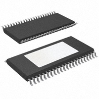
Device Information(1)
PART NUMBER
PACKAGE
TAS5352A
BODY SIZE (NOM)
HTSSOP (44)
14.00 mm × 6.10 mm
(1) For all available packages, see the orderable addendum at
the end of the data sheet.
BTL Output Power vs Supply Voltage
150
TC = 75°C
THD+N at 10%
140
130
120
110
PO – Output Power – W
1
4Ω
100
90
80
6Ω
70
60
50
40
30
8Ω
20
10
0
0
2
4
6
8 10 12 14 16 18 20 22 24 26 28 30 32 34
PVDD – Supply Voltage – V
1
An IMPORTANT NOTICE at the end of this data sheet addresses availability, warranty, changes, use in safety-critical applications,
intellectual property matters and other important disclaimers. PRODUCTION DATA.
�TAS5352A
SLES239A – NOVEMBER 2008 – REVISED DECEMBER 2016
www.ti.com
Table of Contents
1
2
3
4
5
6
7
Features ..................................................................
Applications ...........................................................
Description .............................................................
Revision History.....................................................
Pin Configuration and Functions .........................
Specifications.........................................................
1
1
1
2
3
5
6.1
6.2
6.3
6.4
6.5
6.6
6.7
6.8
6.9
5
5
5
6
6
7
8
8
9
Absolute Maximum Ratings ......................................
ESD Ratings..............................................................
Recommended Operating Conditions.......................
Thermal Information ..................................................
Electrical Characteristics...........................................
Audio Specifications (BTL)........................................
Audio Specifications (Single-Ended Output).............
Audio Specifications (PBTL) .....................................
Typical Characteristics ..............................................
Detailed Description ............................................ 12
7.1 Overview ................................................................. 12
7.2 Functional Block Diagram ....................................... 13
7.3 Feature Description................................................. 14
7.4 Device Functional Modes........................................ 17
8
Application and Implementation ........................ 18
8.1 Application Information............................................ 18
8.2 Typical Applications ................................................ 18
8.3 System Example ..................................................... 24
9 Power Supply Recommendations...................... 25
10 Layout................................................................... 26
10.1 Layout Guidelines ................................................. 26
10.2 Layout Example .................................................... 27
11 Device and Documentation Support ................. 28
11.1
11.2
11.3
11.4
11.5
11.6
11.7
Device Support......................................................
Documentation Support ........................................
Receiving Notification of Documentation Updates
Community Resources..........................................
Trademarks ...........................................................
Electrostatic Discharge Caution ............................
Glossary ................................................................
28
28
28
28
28
28
28
12 Mechanical, Packaging, and Orderable
Information ........................................................... 28
4 Revision History
NOTE: Page numbers for previous revisions may differ from page numbers in the current version.
Changes from Original (November 2008) to Revision A
Page
•
Added ESD Ratings table, Feature Description section, Device Functional Modes, Application and Implementation
section, Power Supply Recommendations section, Layout section, Device and Documentation Support section, and
Mechanical, Packaging, and Orderable Information section .................................................................................................. 1
•
Deleted Ordering Information table, see POA at the end of this data sheet .......................................................................... 5
•
Deleted Package Heat Dissipation Ratings table................................................................................................................... 5
•
Updated values in the Thermal Information table to align with JEDEC standards ................................................................ 6
2
Submit Documentation Feedback
Copyright © 2008–2016, Texas Instruments Incorporated
Product Folder Links: TAS5352A
�TAS5352A
www.ti.com
SLES239A – NOVEMBER 2008 – REVISED DECEMBER 2016
5 Pin Configuration and Functions
DDV Package
44-Pin HTSSOP
Top View
GVDD_B
1
44
GVDD_A
OTW
2
43
BST_A
NC
3
42
NC
NC
4
41
PVDD_A
SD
5
40
PVDD_A
PWM_A
6
39
OUT_A
RESET_AB
7
38
GND_A
PWM_B
8
37
GND_B
OC_ADJ
9
36
OUT_B
GND
10
35
PVDD_B
AGND
11
34
BST_B
33
BST_C
Thermal
VREG
12
M3
13
32
PVDD_C
M2
14
31
OUT_C
M1
15
30
GND_C
PWM_C
16
29
GND_D
RESET_CD
17
28
OUT_D
PWM_D
18
27
PVDD_D
NC
19
26
PVDD_D
NC
20
25
NC
VDD
21
24
BST_D
GVDD_C
22
23
GVDD_D
Pad
Not to scale
Pin Functions
PIN
TYPE (1)
DESCRIPTION
NAME
NO.
AGND
11
P
Analog ground
BST_A
43
P
Bootstrap pin, A-Side
BST_B
34
P
Bootstrap pin, B-Side
BST_C
33
P
Bootstrap pin, C-Side
BST_D
24
P
Bootstrap pin, D-Side
GND
10
P
Ground
GND_A
38
P
Power ground for half-bridge A
(1)
I = Input, O = Output, P = Power
Submit Documentation Feedback
Copyright © 2008–2016, Texas Instruments Incorporated
Product Folder Links: TAS5352A
3
�TAS5352A
SLES239A – NOVEMBER 2008 – REVISED DECEMBER 2016
www.ti.com
Pin Functions (continued)
PIN
TYPE (1)
DESCRIPTION
NAME
NO.
GND_B
37
P
Power ground for half-bridge B
GND_C
30
P
Power ground for half-bridge C
GND_D
29
P
Power ground for half-bridge D
GVDD_A
44
P
Gate-drive voltage supply; A-Side
GVDD_B
1
P
Gate-drive voltage supply; B-Side
GVDD_C
22
P
Gate-drive voltage supply; C-Side
GVDD_D
23
P
Gate-drive voltage supply; D-Side
M1
15
I
Mode selection pin (LSB)
M2
14
I
Mode selection pin
M3
13
I
Mode selection pin (MSB)
NC
3, 4, 19, 20, 25, 42
–
No connect. Pins may be grounded.
OC_ADJ
9
O
Analog overcurrent programming pin
OTW
2
O
Overtemperature warning signal, open-drain, active-low
OUT_A
39
O
Output, half-bridge A
OUT_B
36
O
Output, half-bridge B
OUT_C
31
O
Output, half-bridge C
OUT_D
28
O
Output, half-bridge D
PVDD_A
40, 41
P
Power supply input for half-bridge A
PVDD_B
35
P
Power supply input for half-bridge B
PVDD_C
32
P
Power supply input for half-bridge C
PVDD_D
26, 27
P
Power supply input for half-bridge D
PWM_A
6
I
PWM Input signal for half-bridge A
PWM_B
8
I
PWM Input signal for half-bridge B
PWM_C
16
I
PWM Input signal for half-bridge C
PWM_D
18
I
PWM Input signal for half-bridge D
RESET_AB
7
I
Reset signal for half-bridge A and half-bridge B, active-low
RESET_CD
17
I
Reset signal for half-bridge C and half-bridge D, active-low
SD
5
O
Shutdown signal, open-drain, active-low
VDD
21
P
Input power supply
VREG
12
P
Internal voltage regulator
4
Submit Documentation Feedback
Copyright © 2008–2016, Texas Instruments Incorporated
Product Folder Links: TAS5352A
�TAS5352A
www.ti.com
SLES239A – NOVEMBER 2008 – REVISED DECEMBER 2016
6 Specifications
6.1 Absolute Maximum Ratings
over operating free-air temperature range (unless otherwise noted) (1)
VDD to AGND
GVDD_X to AGND
PVDD_X to GND_X
(2)
MIN
MAX
UNIT
–0.3
13.2
V
–0.3
13.2
V
–0.3
53
V
OUT_X to GND_X
(2)
–0.3
53
V
BST_X to GND_X
(2)
–0.3
66.2
V
–0.3
53
V
VREG to AGND
–0.3
4.2
V
GND_X to GND
–0.3
0.3
V
GND_X to AGND
–0.3
0.3
V
GND to AGND
–0.3
0.3
V
PWM_X, OC_ADJ, M1, M2, M3 to AGND
–0.3
4.2
V
RESET_X, SD, OTW to AGND
–0.3
7
V
9
mA
BST_X to GVDD_X
(2)
Maximum continuous sink current (SD, OTW)
Minimum pulse duration, low
30
ns
Lead temperature, 1.6 mm (1/16 inch) from case (10 s)
Maximum operating junction temperature, TJ
Storage temperature, Tstg
(1)
(2)
260
°C
0
125
°C
–40
125
°C
Stresses beyond those listed under Absolute Maximum Ratings may cause permanent damage to the device. These are stress ratings
only, which do not imply functional operation of the device at these or any other conditions beyond those indicated under Recommended
Operating Conditions. Exposure to absolute-maximum-rated conditions for extended periods may affect device reliability.
These voltages represent the DC voltage + peak AC waveform measured at the terminal of the device in all conditions.
6.2 ESD Ratings
VALUE
V(ESD)
(1)
(2)
Electrostatic discharge
Human-body model (HBM), per ANSI/ESDA/JEDEC JS-001
(1)
±2500
Charged-device model (CDM), per JEDEC specification JESD22-C101 (2)
±750
UNIT
V
JEDEC document JEP155 states that 500-V HBM allows safe manufacturing with a standard ESD control process.
JEDEC document JEP157 states that 250-V CDM allows safe manufacturing with a standard ESD control process.
6.3 Recommended Operating Conditions
MIN
NOM
MAX
UNIT
PVDD_X
Half-bridge supply voltage
0
34.5
37
V
GVDD_X
Supply voltage for logic regulators and gate-drive circuitry
10.8
12
13.2
V
VDD
Digital regulator supply voltage
10.8
12
13.2
V
RL (BTL)
Resistive load impedance (no cycle-by-cycle current control),
recommended demodulation filter
3
4
RL (SE)
Resistive load impedance (no cycle-by-cycle current control),
recommended demodulation filter
2.25
3
RL (PBTL)
Resistive load impedance (no cycle-by-cycle current control),
recommended demodulation filter
1.5
2
LOutput (BTL)
Output-filter inductance, minimum output inductance under short-circuit condition
5
10
LOutput (SE)
Output-filter inductance, minimum output inductance under short-circuit condition
5
10
LOutput (PBTL)
Output-filter inductance, minimum output inductance under short-circuit condition
fS
PWM frame rate
tLOW
Minimum low-state pulse duration per PWM Frame, noise shaper enabled
CPVDD
PVDD close decoupling capacitors
5
10
192
384
Ω
μH
432
30
nS
0.1
Submit Documentation Feedback
Copyright © 2008–2016, Texas Instruments Incorporated
Product Folder Links: TAS5352A
kHz
μF
5
�TAS5352A
SLES239A – NOVEMBER 2008 – REVISED DECEMBER 2016
www.ti.com
Recommended Operating Conditions (continued)
MIN
NOM
CBST
Bootstrap capacitor,
selected value supports PWM frame rates from 192 kHz to 432 kHz
ROC
Overcurrent programming resistor, resistor tolerance = 5%
22
22
REXT-PULLUP
External pullup resistor to 3.3 V to 5 V for SD or OTW
3.3
4.7
TJ
Junction temperature
MAX
33
0
UNIT
nF
47
kΩ
kΩ
125
°C
6.4 Thermal Information
TAS5352A
THERMAL METRIC (1)
DDV (HTSSOP)
UNIT
44 PINS
RθJA
Junction-to-ambient thermal resistance
41.1
°C/W
RθJC(top)
Junction-to-case (top) thermal resistance
0.7
°C/W
RθJB
Junction-to-board thermal resistance
18
°C/W
ψJT
Junction-to-top characterization parameter
0.7
°C/W
ψJB
Junction-to-board characterization parameter
17.9
°C/W
RθJC(bot)
Junction-to-case (bottom) thermal resistance
n/a
°C/W
(1)
For more information about traditional and new thermal metrics, see the Semiconductor and IC Package Thermal Metrics application
report.
6.5 Electrical Characteristics
PVDD_x = 34.5 V, GVDD_X = 12 V, VDD = 12 V, TC (Case temperature) = 25°C, and fS = 384 kHz (unless otherwise noted).
PARAMETER
TEST CONDITIONS
MIN
TYP
MAX
UNIT
3
3.3
3.6
Operating, 50% duty cycle
7.2
17
Idle, reset mode
5.5
11
50% duty cycle
8
16
Reset mode
1
1.8
19
25
mA
525
630
μA
INTERNAL VOLTAGE REGULATOR AND CURRENT CONSUMPTION
VREG
Voltage regulator
(only used as a reference node)
IVDD
VDD supply current
IGVDD_X
Gate supply current per half-bridge
IPVDD_X
Half-bridge idle current
VDD = 12 V
50% duty cycle with 10-μH and 470-nF
output filter
Reset mode, no switching
V
mA
mA
OUTPUT STAGE MOSFETS
RDSon,LS
Drain-to-source resistance, low-side
TJ = 25°C, excludes metalization
resistance
80
89
mΩ
RDSon,HS
Drain-to-source resistance, high-side
TJ = 25°C, excludes metalization
resistance
80
89
mΩ
I/O PROTECTION
Vuvp,G
Undervoltage protection limit
9.5
V
Undervoltage protection limit
250
mV
BSTuvpF
Puts device into RESET when BST
voltage falls below limit
5.9
V
BSTuvpR
Brings device out of RESET when
BST voltage rises above limit
7
V
Vuvp,hyst
OTW
(1)
(1)
Overtemperature warning
115
OTWHYST (1)
Temperature drop needed below
OTW temp. for OTW to be inactive
after the OTW event
OTE (1)
Overtemperature error threshold
(1)
6
125
135
25
145
155
°C
°C
165
°C
Specified by design
Submit Documentation Feedback
Copyright © 2008–2016, Texas Instruments Incorporated
Product Folder Links: TAS5352A
�TAS5352A
www.ti.com
SLES239A – NOVEMBER 2008 – REVISED DECEMBER 2016
Electrical Characteristics (continued)
PVDD_x = 34.5 V, GVDD_X = 12 V, VDD = 12 V, TC (Case temperature) = 25°C, and fS = 384 kHz (unless otherwise noted).
PARAMETER
TEST CONDITIONS
MIN
OTE-OTWdifferential (1)
OTE - OTW differential
Temperature delta between OTW and
OTE
OLPC
Overload protection counter
IOC
Overcurrent limit protection
IOCT
Overcurrent response time
tACTIVITY DETECTOR
Time for PWM activity detector to
activate when no PWM is present
Lack of transition of any PWM input
IPD
Output pulldown current of each halfbridge
Connected when RESET is active to
provide bootstrap capacitor charge. Not
used in SE mode.
TYP
MAX
UNIT
30
°C
fS = 384 kHz
1.25
ms
Resistor—programmable, high-end,
ROC = 22 kΩ with 1-mS pulse
10.9
A
150
ns
13.2
μS
3
mA
STATIC DIGITAL SPECIFICATIONS
VIH
High-level input voltage
VIL
Low-level input voltage
ILeakage
Input leakage current
PWM_A, PWM_B, PWM_C, PWM_D,
M1, M2, M3, RESET_AB, RESET_CD
2
V
0.8
V
100
μA
kΩ
OTW/SHUTDOWN (SD)
RINT_PU
Internal pullup resistance, OTW to
VREG, SD to VREG
VOH
High-level output voltage
VOL
Low-level output voltage
IO = 4 mA
0.2
FANOUT
Device fanout OTW, SD
No external pullup
30
Internal pullup resistor
External pullup of 4.7 kΩ to 5 V
20
26
32
3
3.3
3.6
4.5
V
5
0.4
V
Devices
6.6 Audio Specifications (BTL)
Audio performance is recorded as a chipset consisting of a TAS5518 PWM processor (modulation index limited to 97.7%)
and a TAS5352A power stage. PCB and system configuration are in accordance with recommended guidelines. Audio
frequency = 1 kHz, PVDD_x = 34.5 V, GVDD_x = 12 V, RL = 4 Ω, fS = 384 kHz, ROC = 22 kΩ, TC = 75°C, output filter: LDEM =
10 μH, CDEM = 470 nF (unless otherwise noted).
PARAMETER
POMAX
PO
Maximum power output
Unclipped power output
TEST CONDITIONS
MIN
TYP
RL = 4 Ω, 10% THD+N, clipped input signal
125
RL = 6 Ω, 10% THD+N, clipped input signal
100
RL = 8 Ω, 10% THD+N, clipped input signal
76
RL = 4 Ω, 0 dBFS, unclipped input signal
96
RL = 6 Ω, 0 dBFS, unclipped input signal
72
RL = 8 Ω, 0 dBFS, unclipped input signal
57
0 dBFS, AES17 filter
MAX
UNIT
W
0.4%
THD+N
Total harmonic distortion + noise
Vn
Output integrated noise
A-weighted, AES17 filter, Auto mute
disabled
50
μV
SNR
Signal-to-noise ratio (1)
A-weighted, AES17 filter, Auto mute
disabled
110
dB
DNR
Dynamic range
A-weighted, input level = –60 dBFS, AES17
filter
110
dB
DC Offset
Output offset voltage
±15
mV
Pidle
Power dissipation due to idle losses
(IPVDD_X)
2.6
W
(1)
(2)
1 W, AES17 filter
PO = 0 W, all half-bridges switching
0.09%
(2)
SNR is calculated relative to 0-dBFS input level.
Actual system idle losses are affected by core losses of output inductors.
Submit Documentation Feedback
Copyright © 2008–2016, Texas Instruments Incorporated
Product Folder Links: TAS5352A
7
�TAS5352A
SLES239A – NOVEMBER 2008 – REVISED DECEMBER 2016
www.ti.com
6.7 Audio Specifications (Single-Ended Output)
Audio performance is recorded as a chipset consisting of a TAS5086 PWM processor (modulation index limited to 97.7%)
and a TAS5352A power stage. PCB and system configuration are in accordance with recommended guidelines. Audio
frequency = 1 kHz, PVDD_x = 34.5 V, GVDD_x = 12 V, RL = 4 Ω, fS = 384 kHz, ROC = 22 kΩ, TC = 75°C, output filter: LDEM =
20 μH, CDEM = 1 μF (unless otherwise noted).
PARAMETER
POMAX
Maximum power output
PO
Unclipped power output
TEST CONDITIONS
MIN
TYP
RL = 3 Ω, 10% THD+N, clipped input signal
45
RL = 4 Ω, 10% THD+N, clipped input signal
35
RL = 3 Ω, 0 dBFS, unclipped input signal
35
RL = 4 Ω, 0 dBFS, unclipped input signal
MAX
UNIT
W
25
0 dBFS, AES17 filter
0.4%
THD+N
Total harmonic distortion + noise
Vn
Output integrated noise
A-weighted, AES17 filter, Auto mute
disabled
40
μV
SNR
Signal-to-noise ratio (1)
A-weighted, AES17 filter, Auto mute
disabled
109
dB
DNR
Dynamic range
A-weighted, input level = –60 dBFS, AES17
filter
109
dB
Pidle
Power dissipation due to idle losses
(IPVDD_X)
PO = 0 W, all half-bridges switching (2)
2.6
W
(1)
(2)
1 W, AES17 filter
0.09%
SNR is calculated relative to 0-dBFS input level.
Actual system idle losses are affected by core losses of output inductors.
6.8 Audio Specifications (PBTL)
Audio performance is recorded as a chipset consisting of a TAS5518 PWM processor (modulation index limited to 97.7%)
and a TAS5352A power stage. PCB and system configuration are in accordance with recommended guidelines. Audio
frequency = 1 kHz, PVDD_x = 34.5 V, GVDD_x = 12 V, RL = 3 Ω, fS = 384 kHz, ROC = 22 kΩ, TC = 75°C, output filter: LDEM =
10 μH, CDEM = 1 μF (unless otherwise noted).
PARAMETER
POMAX
Maximum power output
PO
Unclipped power output
THD+N
Total harmonic distortion + noise
TEST CONDITIONS
MIN
TYP
RL = 3 Ω, 10% THD+N, clipped input signal
195
RL = 2 Ω, 10% THD+N, clipped input signal
250
RL = 3 Ω, 0 dBFS, unclipped input signal
145
RL = 2 Ω, 0 dBFS, unclipped input signal
0 dBFS, AES17 filter
MAX
UNIT
W
190
0.4%
1 W, AES17 filter
0.09%
Vn
Output integrated noise
A-weighted, AES17 filter, Auto mute
disabled
SNR
Signal-to-noise ratio (1)
A-weighted, AES17 filter, Auto mute
disabled
110
dB
DNR
Dynamic range
A-weighted, input level = –60 dBFS AES17
filter
110
dB
DC Offset
Output offset voltage
±15
mV
Pidle
Power dissipation due to idle losses
(IPVDD_X)
2.6
W
(1)
(2)
8
PO = 0 W, all half-bridges switching
(2)
50
μV
SNR is calculated relative to 0-dBFS input level.
Actual system idle losses are affected by core losses of output inductors.
Submit Documentation Feedback
Copyright © 2008–2016, Texas Instruments Incorporated
Product Folder Links: TAS5352A
�TAS5352A
www.ti.com
SLES239A – NOVEMBER 2008 – REVISED DECEMBER 2016
6.9 Typical Characteristics
6.9.1 BTL Configuration
150
10
TC = 75°C
THD+N at 10%
THD+N – Total Hamonic Distortion – %
5
TC = 75°C
THD+N at 10%
140
130
120
2
110
PO – Output Power – W
1
0.5
4W
0.2
6W
0.1
0.05
4Ω
100
90
80
6Ω
70
60
50
40
30
0.02
0.01
10
0
0.005
20m
50m 100m 200m 500m
1
5
2
10
20
50
100 200
0
4
2
6
PVDD – Supply Voltage – V
Figure 1. Total Harmonic Distortion + Noise
vs Output Power
Figure 2. Output Power vs Supply Voltage
120
115
110
105
100
95
90
85
80
75
70
65
60
55
50
45
40
35
30
25
20
15
10
5
100
95
TC = 75°C
90
85
80
8W
6W
8
75
70
8W
4
65
4W
6W
60
55
50
45
40
35
30
25
20
TC = 25°C
THD+N at 10%
15
8W
10
5
0
0
2
4
6
8 10 12 14 16
0
18 20 22 24 26 28 30 32 34
0
40
80
PVDD – Supply Voltage – V
120
160
200
240
280
2 Channels Output Power – W
Figure 3. Unclipped Output Power
vs Supply Voltage
Figure 4. System Efficiency vs Output Power
160
40
TC = 25°C
THD+N at 10%
38
36
150
140
34
130
32
4W
6
120
4W
30
PO – Output Power – W
28
26
Power Loss – W
8 10 12 14 16 18 20 22 24 26 28 30 32 34
PO – Output Power – W
Efficiency – %
PO – Output Power – W
8Ω
20
8W
24
22
20
18
16
14
4
8W
110
100
90
80
70
60
8W
50
12
8W
6
10
40
8
30
6
20
8W
4
0
0
20
40
60
80
THD+N at 10%
10
2
100 120 140 160 180 200 220 240 260 280
2 Channels Output Power – W
0
10
20
30
40
50
60
70
80
90
100 110 120
TC – Case Temperature – °C
Figure 5. System Power Loss vs Output Power
Figure 6. System Output Power
vs Case Temperature
Submit Documentation Feedback
Copyright © 2008–2016, Texas Instruments Incorporated
Product Folder Links: TAS5352A
9
�TAS5352A
SLES239A – NOVEMBER 2008 – REVISED DECEMBER 2016
www.ti.com
BTL Configuration (continued)
+0
TC = 75°C
VREF = 20.60 V
Sample Rate = 48 kHz
FFT Size = 16384
–10
–20
–30
–40
Noise Amplitude – V
–50
–60
–70
–80
–90
–100
–110
–120
–130
–140
–150
–160
0 1k 2k 3k 4k 5k 6k 7k 8k 9k 10k 11k 12k 13k 14k 15k 16k 17k 18k 19k 20k 21k 22k
f – Frequency – kHz
Figure 7. Noise Amplitude vs Frequency
6.9.2 SE Configuration
5
TC = 75°C
THD+N at 10%
2
PO – Output Power – W
THD+N – Total Hamonic Distortion – %
10
1
0.5
3W
0.2
0.1
0.05
4W
0.02
0.01
0.005
20m
50m 100m 200m 500m
1
2
5
10
20
60
57.5
55
52.5
50
47.5
45
42.5
40
37.5
35
32.5
30
27.5
25
22.5
20
17.5
15
12.5
10
7.5
5
2.5
0
50 80
TC = 75°C
THD+N at 10%
3W
4W
0
2
4
6
8
10 12 14
16 18
20
22 24
26 28 30 32
34
PVDD – Supply Voltage – V
PO – Output Power – W
Figure 9. Output Power vs Supply Voltage
PO – Output Power – W
Figure 8. Total Harmonic Distortion + Noise
vs Output Power
60
57.5
55
52.5
50
47.5
45
42.5
40
37.5
35
32.5
30
27.5
25
22.5
20
17.5
15
12.5
10
7.5
5
2.5
3W
4W
THD+N at 10%
0
10
20
30
40
50
60
70
80
90
100
110
120
TC – Case Temperature – °C
Figure 10. Output Power vs Case Temperature
10
Submit Documentation Feedback
Copyright © 2008–2016, Texas Instruments Incorporated
Product Folder Links: TAS5352A
�TAS5352A
www.ti.com
SLES239A – NOVEMBER 2008 – REVISED DECEMBER 2016
6.9.3 PBTL Configuration
300
5
TC = 75°C
THD+N at 10%
TC = 75°C
THD+N at 10%
280
4W
260
240
2
4W
2
220
1
PO – Output Power – W
THD+N – Total Hamonic Distortion – %
10
0.5
2W
0.2
0.1
0.05
3W
180
160
3W
4
140
120
100
4W
80
60
0.02
40
8W
0.01
0.005
20m
200
8W
20
0
50m 100m 200m 500m 1
2
5
10
20
50
0
100 200 400
2
4
6
8
10 12 14 16 18 20 22 24 26
28 30 32
34
PVDD – Supply Voltage – V
PO – Output Power – W
Figure 12. Output Power vs Supply Voltage
Figure 11. Total Harmonic Distortion + Noise
vs Output Power
300
280
260
4W
3
240
8W
2
220
PO – Output Power – W
200
180
160
140
120
8W
4
100
80
60
40
8W
THD+N at 10%
20
0
10
20
30
40
50
60
70
80
90
100
110
120
TC – Case Temperature – °C
Figure 13. System Output Power vs Case Temperature
Submit Documentation Feedback
Copyright © 2008–2016, Texas Instruments Incorporated
Product Folder Links: TAS5352A
11
�TAS5352A
SLES239A – NOVEMBER 2008 – REVISED DECEMBER 2016
www.ti.com
7 Detailed Description
7.1 Overview
The TAS5352A is a PWM input, Class-D audio amplifier. The output of the TAS5352A can be configured for
single-ended, bridge-tied load (BTL), or parallel BTL (PBTL) output. The independent supply rails provide
improved audio performance: one for audio power output (PVDD) and the other for gate drive and analog control
(GVDD and VDD).
The TAS5352A contains a protection system that safeguards the device against short circuits, overload,
overtemperature, and undervoltage conditions. An error reporting system provides feedback under fault
conditions.
Figure 14 shows typical connections for BTL outputs. A detailed schematic can be viewed in TAS5352A EVM
User's Guide (SLAU244).
12
Submit Documentation Feedback
Copyright © 2008–2016, Texas Instruments Incorporated
Product Folder Links: TAS5352A
�TAS5352A
www.ti.com
SLES239A – NOVEMBER 2008 – REVISED DECEMBER 2016
7.2 Functional Block Diagram
VDD
4
Undervoltage
Protection
OTW
Internal Pullup
Resistors to VREG
SD
M1
Protection
and
I/O Logic
M2
M3
4
VREG
VREG
Power
On
Reset
AGND
Temp.
Sense
GND
RESET_AB
Overload
Protection
RESET_CD
OC_ADJ
Isense
GVDD_D
BST_D
PVDD_D
PWM_D
PWM
Rcv.
Ctrl.
Timing
Gate
Drive
OUT_D
BTL/PBTL−Configuration
Pulldown Resistor
GND_D
GVDD_C
BST_C
PVDD_C
PWM_C
PWM
Rcv.
Ctrl.
Timing
Gate
Drive
OUT_C
BTL/PBTL−Configuration
Pulldown Resistor
GND_C
GVDD_B
BST_B
PVDD_B
PWM_B
PWM
Rcv.
Ctrl.
Timing
Gate
Drive
OUT_B
BTL/PBTL−Configuration
Pulldown Resistor
GND_B
GVDD_A
BST_A
PVDD_A
PWM_A
PWM
Rcv.
Ctrl.
Timing
Gate
Drive
OUT_A
BTL/PBTL−Configuration
Pulldown Resistor
GND_A
B0034-03
Copyright © 2016, Texas Instruments Incorporated
Submit Documentation Feedback
Copyright © 2008–2016, Texas Instruments Incorporated
Product Folder Links: TAS5352A
13
�TAS5352A
SLES239A – NOVEMBER 2008 – REVISED DECEMBER 2016
www.ti.com
7.3 Feature Description
7.3.1 System Power-Up and Power-Down Sequence
7.3.1.1 Powering Up
The TAS5352A does not require a power-up sequence. The outputs of the H-bridges remain in a highimpedance state until the gate-drive supply voltage (GVDD_X) and VDD voltage are above the undervoltage
protection (UVP) voltage threshold (see the Electrical Characteristics). Although not specifically required, TI
recommends holding RESET_AB and RESET_CD in a low state while powering up the device. This allows an
internal circuit to charge the external bootstrap capacitors by enabling a weak pulldown of the half-bridge output.
When the TAS5352A is being used with TI PWM modulators such as the TAS5518, no special attention to the
state of RESET_AB and RESET_CD is required, provided that the chipset is configured as recommended.
7.3.1.2 Powering Down
The TAS5352A does not require a power-down sequence. The device remains fully operational as long as the
gate-drive supply (GVDD_X) voltage and VDD voltage are above the undervoltage protection (UVP) voltage
threshold (see the Electrical Characteristics). Although not specifically required, it is a good practice to hold
RESET_AB and RESET_CD low during power down, thus preventing audible artifacts including pops or clicks.
When the TAS5352A is being used with TI PWM modulators such as the TAS5518, no special attention to the
state of RESET_AB and RESET_CD is required, provided that the chipset is configured as recommended.
7.3.2 Mid Z Sequence Compatibility
The TAS5352A is compatible with the Mid Z Sequence of the TAS5086 modulator. The Mid Z Sequence is a
series of pulses that is generated by the modulator. This sequence causes the power stage to slowly enable its
outputs as it begins to switch.
By slowly starting the PWM switching, the impulse response created by the onset of switching is reduced. This
impulse response is the acoustic artifact that is heard in the output transducers (loudspeakers) and is commonly
termed click or pop.
The low acoustic artifact noise of the TAS5352A will be further decreased when used in conjunction with the
TAS5086 modulator with the Mid Z Sequence enabled.
The Mid Z Sequence is primarily used for the single-ended output configuration. It facilitates a softer PWM output
start after the split cap output configuration is charged.
7.3.3 Error Reporting
The SD and OTW pins are both active-low, open-drain outputs. Their function is for protection-mode signaling to
a PWM controller or other system-control device.
Any fault resulting in device shutdown is signaled by the SD pin going low. Likewise, OTW goes low when the
device junction temperature exceeds 125°C (see Table 1).
Table 1. Error Reporting
SD
OTW
0
0
Overtemperature (OTE) or overload (OLP) or undervoltage (UVP)
DESCRIPTION
0
1
Overload (OLP) or undervoltage (UVP)
1
0
Junction temperature higher than 125°C (overtemperature warning)
1
1
Junction temperature lower than 125°C and no OLP or UVP faults (normal operation)
Note that asserting either RESET_AB or RESET_CD low forces the SD signal high, independent of faults being
present. TI recommends monitoring the OTW signal using the system microcontroller and responding to an
overtemperature warning signal by, for example, turning down the volume to prevent further heating of the device
resulting in device shutdown (OTE).
To reduce external component count, an internal pullup resistor to 3.3 V is provided on both SD and OTW
outputs. Level compliance for 5-V logic can be obtained by adding external pullup resistors to 5 V (see the
Electrical Characteristics table for further specifications).
14
Submit Documentation Feedback
Copyright © 2008–2016, Texas Instruments Incorporated
Product Folder Links: TAS5352A
�TAS5352A
www.ti.com
SLES239A – NOVEMBER 2008 – REVISED DECEMBER 2016
7.3.4 Device Protection System
The TAS5352A contains advanced protection circuitry carefully designed to facilitate system integration and ease
of use, as well as to safeguard the device from permanent failure due to a wide range of fault conditions such as
short circuits, overload, overtemperature, and undervoltage. The TAS5352A responds to a fault by immediately
setting the power stage in a high-impedance (Hi-Z) state and asserting the SD pin low. In situations other than
overload and overtemperature error (OTE), the device automatically recovers when the fault condition has been
removed, that is, the supply voltage has increased.
The device will function on errors, as shown in Table 2.
Table 2. Device Protection
BTL MODE
LOCAL ERROR
IN
A
B
C
D
PBTL MODE
TURNS OFF
LOCAL ERROR
IN
A+B
C+D
TURNS OFF
A
B
C
SE MODE
LOCAL ERROR
IN
TURNS OFF
A
A+B+C+D
D
B
C
D
A+B
C+D
Bootstrap UVP does not shutdown according to Table 2, it shuts down the respective half-bridge.
7.3.4.1 Use of TAS5352A in High-Modulation-Index Capable Systems
This device requires at least 30 ns of low time on the output per 384-kHz PWM frame rate to keep the bootstrap
capacitors charged. As an example, if the modulation index is set to 99.2% in the TAS5508, this setting allows
PWM pulse durations down to 10 ns. This signal, which does not meet the 30-ns requirement, is sent to the
PWM_X pin and this low-state pulse time does not allow the bootstrap capacitor to stay charged. The TAS5352A
device requires limiting the TAS5508 modulation index to 97.7% to keep the bootstrap capacitor charged under
all signals and loads.
The TAS5352A contains a bootstrap capacitor undervoltage protection circuit (BST_UVP) that monitors the
voltage on the bootstrap capacitors. When the voltage on the bootstrap capacitors is less than required for
proper control of the high-side MOSFETs, the device initiates the bootstrap capacitor recharge sequences until
the bootstrap capacitors are properly charged for robust operation. This function may be activated with PWM
pulses less than 30 ns.
Therefore, TI strongly recommends using a TI PWM processor, such as TAS5518, TAS5086, or TAS5508, with
the modulation index set at 97.7% to interface with TAS5352A.
7.3.4.2 Overcurrent (OC) Protection With Current Limiting and Overload Detection
The device has independent, fast-reacting current detectors with programmable trip threshold (OC threshold) on
all high-side and low-side power-stage FETs. See Table 3 for OC-adjust resistor values. The detector outputs are
closely monitored by two protection systems. The first protection system controls the power stage to prevent the
output current from further increasing, that is, it performs a current-limiting function rather than prematurely
shutting down during combinations of high-level music transients and extreme speaker load impedance drops. If
the high-current situation persists, that is, the power stage is being overloaded, a second protection system
triggers a latching shutdown, resulting in the power stage being set in the high-impedance (Hi-Z) state. Current
limiting and overload protection are independent for half-bridges A and B and, respectively, C and D. That is, if
the bridge-tied load between half-bridges A and B causes an overload fault, only half-bridges A and B are shut
down.
• For the lowest-cost bill of materials in terms of component selection, the OC threshold measure should be
limited, considering the power output requirement and minimum load impedance. Higher-impedance loads
require a lower OC threshold.
• The demodulation-filter inductor must retain at least 5 μH of inductance at twice the OC threshold setting.
Unfortunately, most inductors have decreasing inductance with increasing temperature and increasing current
(saturation). To some degree, an increase in temperature naturally occurs when operating at high output
currents, due to core losses and the DC resistance of the copper winding of the inductor. A thorough analysis of
inductor saturation and thermal properties is strongly recommended.
Submit Documentation Feedback
Copyright © 2008–2016, Texas Instruments Incorporated
Product Folder Links: TAS5352A
15
�TAS5352A
SLES239A – NOVEMBER 2008 – REVISED DECEMBER 2016
www.ti.com
Setting the OC threshold too low might cause issues such as lack of enough output power or unexpected
shutdowns due to too-sensitive overload detection.
In general, TI recommends following the external component selection and PCB layout in the Detailed Design
Procedure closely.
For added flexibility, the OC threshold is programmable within a limited range using a single external resistor
connected between the OC_ADJ pin and AGND. See the Electrical Characteristics table for information on the
correlation between programming-resistor value and the OC threshold.
NOTE
A properly functioning overcurrent detector assumes the presence of a properly designed
demodulation filter at the power-stage output. It is required to follow the guidelines in
Table 3 when selecting the OC threshold and an appropriate demodulation inductor.
Table 3. Overcurrent Resistor Selection
OC-ADJUST RESISTOR VALUES (kΩ)
MAX CURRENT BEFORE OC OCCURS (A), TC = 75°C
22
10.9
33
9.1
47
7.1
The reported maximum peak current in the table above is measured with continuous current in 1 Ω, one channel
active and the other one muted.
7.3.4.3 Pin-to-Pin Short-Circuit Protection (PPSC)
The PPSC detection system protects the device from permanent damage in the case that a power output pin
(OUT_X) is shorted to GND_X or PVDD_X. For comparison the OC protection system detects an over current
after the demodulation filter where PPSC detects shorts directly at the pin before the filter. PPSC detection is
performed at start-up, that is, when VDD is supplied, consequently a short to either GND_X or PVDD_X after
system start-up does not activate the PPSC detection system. When PPSC detection is activated by a short on
the output, all half-bridges are kept in a Hi-Z state until the short is removed, the device then continues the startup sequence and starts switching. The detection is controlled globally by a two-step sequence. The first step
ensures that there are no shorts from OUT_X to GND_X, the second step tests that there are no shorts from
OUT_X to PVDD_X. The total duration of this process is roughly proportional to the capacitance of the output LC
filter. The typical duration is < 15 ms/μF. While the PPSC detection is in progress, SD is kept low and the device
does not react to changes applied to the RESET pins. If no shorts are present the PPSC detection passes, and
SD is released. A device reset will not start a new PPSC detection. PPSC detection is enabled in BTL and PBTL
output configurations, the detection is not performed in SE mode. To make sure not to trip the PPSC detection
system, TI recommends not to insert any resistive load to GND_X or PVDD_X.
7.3.4.4 Overtemperature Protection
The TAS5352A has a two-level temperature-protection system that asserts an active-low warning signal (OTW)
when the device junction temperature exceeds 125°C (typical) and, if the device junction temperature exceeds
155°C (typical), the device is put into thermal shutdown, resulting in all half-bridge outputs being set in the highimpedance (Hi-Z) state and SD being asserted low. OTE is latched in this case. To clear the OTE latch, either
RESET_AB or RESET_CD must be asserted. Thereafter, the device resumes normal operation.
7.3.4.5 Undervoltage Protection (UVP) and Power-On-Reset (POR)
The UVP and POR circuits of the TAS5352A fully protect the device in any power up, power down, or brownout
situations. While powering up, the POR circuit resets the overload circuit (OLP) and ensures that all circuits are
fully operational when the GVDD_X and VDD supply voltages reach stated in the Electrical Characteristics.
Although GVDD_X and VDD are independently monitored, a supply voltage drop below the UVP threshold on
any VDD or GVDD_X pin results in all half-bridge outputs immediately being set in the high-impedance (Hi-Z)
state and SD being asserted low. The device automatically resumes operation when all supply voltages have
increased above the UVP threshold.
16
Submit Documentation Feedback
Copyright © 2008–2016, Texas Instruments Incorporated
Product Folder Links: TAS5352A
�TAS5352A
www.ti.com
SLES239A – NOVEMBER 2008 – REVISED DECEMBER 2016
7.3.5 Device Reset
Two reset pins are provided for independent control of half-bridges A/B and C/D. When RESET_AB is asserted
low, all four power-stage FETs in half-bridges A and B are forced into a high-impedance (Hi-Z) state. Likewise,
asserting RESET_CD low forces all four power-stage FETs in half-bridges C and D into a high-impedance state.
Thus, both reset pins are well suited for hard-muting the power stage, if needed.
In BTL modes, to accommodate bootstrap charging prior to switching start, asserting the reset inputs low enables
weak pulldown of the half-bridge outputs. In the SE mode, the weak pulldowns are not enabled. Therefore, TI
recommends ensuring bootstrap capacitor charging by providing a low pulse on the PWM inputs when reset is
asserted high.
Asserting either reset input low removes any fault information to be signaled on the SD output, that is, SD is
forced high.
A rising-edge transition on either reset input allows the device to resume operation after an overload fault. To
ensure thermal reliability, the rising edge of reset must occur no sooner than 4 ms after the falling edge of SD.
7.4 Device Functional Modes
7.4.1 Protection MODE Selection Pins
Protection modes are selected by shorting M1, M2, and M3 to VREG or GND.
Table 4. Protection Mode Selection Pins
MODE PINS
(1)
(2)
(3)
MODE NAME
PWM INPUT (1)
0
BTL mode 1
2N
All protection systems enabled
1
BTL mode 2
2N
Latching shutdown on, PWM activity detector and OLP disabled
0
BTL mode 3
1N
M3
M2
M1
0
0
0
0
0
1
1N / 2N
DESCRIPTION
All protection systems enabled
(2)
0
1
1
PBTL mode
1
0
0
SE mode 1
1N
All protection systems enabled
All protection systems enabled (3)
1
0
1
SE mode 2
1N
Latching shutdown on, PWM activity detector and OLP disabled (3)
1
1
0
1
1
1
Reserved
The 1N and 2N naming convention is used to indicate the number of PWM lines to the power stage per channel in a specific mode.
PWM_D is used to select between the 1N and 2N interface in PBTL mode (Low = 1N; High = 2N). PWM_D is internally pulled low in
PBTL mode. PWM_A is used as the PWM input in 1N mode and PWM_A and PWM_B are used as inputs for the 2N mode.
PPSC detection system disabled.
Submit Documentation Feedback
Copyright © 2008–2016, Texas Instruments Incorporated
Product Folder Links: TAS5352A
17
�TAS5352A
SLES239A – NOVEMBER 2008 – REVISED DECEMBER 2016
www.ti.com
8 Application and Implementation
NOTE
Information in the following applications sections is not part of the TI component
specification, and TI does not warrant its accuracy or completeness. TI’s customers are
responsible for determining suitability of components for their purposes. Customers should
validate and test their design implementation to confirm system functionality.
8.1 Application Information
The TAS5352A can be configured either in stereo BTL mode, 4 channel SE mode, or mono PBTL mode,
depending on output power conditions and system design.
8.2 Typical Applications
8.2.1 BTL Application With AD Modulation Filters – 2N
GVDD (+12 V)
PVDD
2.2 W
2.2 W
3.3 W
470 µF
50 V
100 nF
100 nF
10 nF
50 V
TAS5352ADDV
GND
GND
GVDD_A
GVDD_B
Microcontroller
I2C
GND
PWM1_P
VALID
PWM1_M
22 k
NC
NC
NC
PVDD_A
SD
PVDD_A
PWM_A
OUT_A
RESET_AB
GND_A
PWM_B
GND_B
OC_ADJ
OUT_B
BST_C
VREG
PWM2_P
M3
PVDD_C
M2
OUT_C
M1
GND_C
PWM_C
GND_D
TAS5508/18
0W
PWM_D
PVDD_D
NC
PVDD_D
100 nF
50 V
GND
1 nF
50 V
GND
10 nF
50 V
3.3 W
10 µH
10 µH
33 nF 25V
GVDD_D
GVDD_C
GND
3.3 W
1 nF
50 V
100 nF
50 V
10 nF
50 V
100 nF
50 V
470 nF
100 nF
50 V
100 nF
50 V
GND
1 nF
50 V
GND
GND
10 nF
50 V
3.3 W
10 µH
33 nF 25 V
PVDD
3.3 W
GND
470 µF
50 V
10 nF
50 V
100 nF
100 nF
2.2 W
2.2 W
VDD (+12 V)
10 nF
50 V
BST_D
VDD
100 nF
100 nF
50 V
470 nF
100 nF
50 V
33 nF 25 V
NC
NC
GND
GND
OUT_D
RESET_CD
PWM2_M
100 nF
50 V
3.3 W
1 nF
50 V
BST_B
AGND
100 nF
33 nF 25 V
GND
PVDD_B
GND
GND
GND
10 µH
BST_A
OTW
GND
GND
GND
GVDD (+12 V)
Copyright © 2016, Texas Instruments Incorporated
Figure 14. Typical Differential (2N) BTL Application With AD Modulation Filters
8.2.1.1 Design Requirements
Table 5 lists the design requirements for this example.
Table 5. Design Requirements for Typical Differential BTL
18
DESIGN PARAMETER
EXAMPLE
Low Power (Pullup) Supply
3.3 V
Mid Power Supply (GVDD, VDD)
12 V
High Power Supply (PVDD)
12 – 36 V
Submit Documentation Feedback
Copyright © 2008–2016, Texas Instruments Incorporated
Product Folder Links: TAS5352A
�TAS5352A
www.ti.com
SLES239A – NOVEMBER 2008 – REVISED DECEMBER 2016
Table 5. Design Requirements for Typical Differential BTL (continued)
DESIGN PARAMETER
EXAMPLE
INPUT A = 0 – 3.3 V PWM
INPUT_B = 0 – 3.3 V PWM
PWM Inputs
INPUT_C = 0 – 3.3 V PWM
INPUT_D = 0 – 3.3 V PWM
4–8Ω
Speaker Impedance
8.2.1.2 Detailed Design Procedure
8.2.1.2.1 PCB Material Recommendation
FR-4 Glass Epoxy material with 2-oz. (70-μm) copper is recommended when using the TAS5352A. The use of
this material can provide for higher power output, improved thermal performance, and better EMI margin (due to
lower PCB trace inductance).
8.2.1.2.2 PVDD Capacitor Recommendation
The large capacitors used in conjunction with each full-bridge, are referred to as the PVDD Capacitors. These
capacitors should be selected for proper voltage margin and adequate capacitance to support the power
requirements. In practice, with a well designed system power supply, 1000-μF, 50-V capacitors will support more
applications. The PVDD capacitors should be low-ESR type because they are used in a circuit associated with
high-speed switching.
8.2.1.2.3 Decoupling Capacitor Recommendations
To design an amplifier that has robust performance, passes regulatory requirements, and exhibits good audio
performance, good-quality decoupling capacitors should be used. In practice, X7R should be used in this
application.
The voltage of the decoupling capacitors should be selected in accordance with good design practices.
Temperature, ripple current, and voltage overshoot must be considered. This fact is particularly true in the
selection of the 0.1 μF that is placed on the power supply to each half-bridge. It must withstand the voltage
overshoot of the PWM switching, the heat generated by the amplifier during high power output, and the ripple
current created by high power output. A minimum voltage rating of 50 V is required for use with a 34.5-V power
supply.
Detailed information regarding LC filter design and the impact on amplifier performance can be found in the
application note LC Filter Design (SLAA701).
8.2.1.3 Application Curves
Relevant performance plots for TAS5352A in BTL configuration are shown in BTL Configuration.
Table 6. Relevant Performance Plots, BTL Configuration
PLOT TITLE
FIGURE NUMBER
Total Harmonic Distortion + Noise vs. Output power
Figure 1
Output Power vs. Supply Voltage
Figure 2
Unclipped Output Power vs. Supply Voltage
Figure 3
System Efficiency vs. Output Power
Figure 4
System Power Loss vs. Output Power
Figure 5
System Output Power vs. Case Temperature
Figure 6
Noise Amplitude vs. Frequency
Figure 7
Submit Documentation Feedback
Copyright © 2008–2016, Texas Instruments Incorporated
Product Folder Links: TAS5352A
19
�TAS5352A
SLES239A – NOVEMBER 2008 – REVISED DECEMBER 2016
www.ti.com
8.2.2 BTL Application With AD Modulation Filters – 1N
GVDD (+12 V)
PVDD
2.2 W
2.2 W
3.3 W
470 µF
50 V
100 nF
100 nF
10 nF
50 V
TAS5352ADDV
GND
GND
GVDD_A
GVDD_B
Microcontroller
I2C
GND
PWM1_P
VALID
22 k
NC
NC
NC
PVDD_A
SD
PVDD_A
PWM_A
OUT_A
RESET_AB
GND_A
PWM_B
GND_B
OC_ADJ
OUT_B
BST_C
VREG
PWM2_P
M3
PVDD_C
M2
OUT_C
M1
GND_C
PWM_C
GND_D
0W
PWM_D
PVDD_D
NC
PVDD_D
100 nF
50 V
GND
1 nF
50 V
GND
10 nF
50 V
3.3 W
10 µH
10 µH
33 nF 25V
GVDD_D
GVDD_C
GND
3.3 W
1 nF
50 V
100 nF
50 V
10 nF
50 V
100 nF
50 V
470 nF
100 nF
50 V
GND
100 nF
50 V
1 nF
50 V
GND
GND
10 nF
50 V
3.3 W
10 µH
33 nF 25 V
PVDD
3.3 W
GND
470 µF
50 V
10 nF
50 V
100 nF
100 nF
2.2 W
VDD (+12 V)
10 nF
50 V
BST_D
VDD
100 nF
100 nF
50 V
470 nF
100 nF
50 V
33 nF 25 V
NC
NC
GND
GND
OUT_D
RESET_CD
TAS5508/18
100 nF
50 V
3.3 W
1 nF
50 V
BST_B
AGND
100 nF
33 nF 25 V
GND
PVDD_B
GND
GND
GND
10 µH
BST_A
OTW
2.2 W
GND
GND
GND
GVDD (+12 V)
Copyright © 2016, Texas Instruments Incorporated
Figure 15. Typical Non-Differential (1N) BTL Application With AD Modulation Filters
8.2.2.1 Design Requirements
Table 7 lists the design requirements for this example.
Table 7. Design Requirements for Typical Non-Differential BTL
DESIGN PARAMETER
EXAMPLE
Low Power (Pullup) Supply
3.3 V
Mid Power Supply (GVDD, VDD)
12 V
High Power Supply (PVDD)
12 – 36 V
INPUT A = 0 – 3.3 V PWM
PWM Inputs
INPUT_B = N/C
INPUT_C = 0 – 3.3 V PWM
INPUT_D = N/C
4–8Ω
Speaker Impedance
20
Submit Documentation Feedback
Copyright © 2008–2016, Texas Instruments Incorporated
Product Folder Links: TAS5352A
�TAS5352A
www.ti.com
SLES239A – NOVEMBER 2008 – REVISED DECEMBER 2016
8.2.3 SE Application
2
GND
2
100nF
PWM3_P
PWM4_P
1
0R
GND
2
1
TAS5508/18
OUT_A
RESET_AB
GND_A
PWM_B
GND_B
OC_ADJ
OUT_B
GND
PVDD_B
AGND
BST_B
VREG
BST_C
M3
PVDD_C
M2
OUT_C
M1
GND_C
PWM_C
GND_D
RESET_CD
OUT_D
PWM_D
PVDD_D
NC
PVDD_D
NC
NC
VDD
BST_D
GVDD_D
GND
2
GND
100nF
50V
100nF
50V
33nF25V
1
2
1
2
33nF25V
1
1
20uH
2
2
B
C
2
D
20uH
GND
100nF
50V
100nF
50V
GND
1
2
33nF25V
1
20uH
3.3R GND
2
2
1
12
1
2
GND
1
1
2
1
2
3.3R
2
2
GND
10k
1%
2
3.3R
1
100nF
50V
2
2
470uF
50V
10k
1%
100nF
50V
1
1
2
470uF
50V
1
2
GND
1
50V
10nF GND
10nF
50V
1
2
3.3R GND
2
2
3.3R GND
2
1
12
100nF
50V
2
100nF
50V
GND
1
1
2
3.3R
2
1
2
50V
10nF GND
10k
1%
2
3.3R
GND
2
1
470uF
50V
10k
1%
2
470uF
50V
2
GND
1
100nF
50V
1uF
10k
1
12
PVDD
2
2
1
100nF
50V
2
1
2
2
2
10k
1%
1
470uF
50V
10k
1%
2
470uF
50V
2
1
PVDD
1uF
10k
1
D
1
C
1
2
50V
10nF GND
10nF
50V
1
2
1
2
PVDD
GND
1uF
10k
2
1
12
2
1
2
1
2
1
100nF
50V
10k
1%
470uF
50V
GVDD (+12V)
1
1
10nF
50V
1
2
B
100nF
50V
1
2
10k
1%
2
1
1uF
10k
1
2
GND
GND
3.3R GND
A
10nF
50V
2
2
100nF
10nF
50V
1
2
470uF
50V
PVDD
3.3R
1
GND
VDD (+12V)
470uF
50V
1
1
2.2R
1
2.2R
2
100nF
2
1
2
GND
PVDD
A
1
GVDD_C
2
2
PVDD_A
PWM_A
20uH
1
PVDD_A
SD
1
1 2
NC
GND
1
2
33nF25V
GND
2
100nF
NC
44
43
42
41
40
39
38
37
36
35
34
33
32
31
30
29
28
27
26
25
24
23
2
1 22k 2
BST_A
NC
10nF
50V
1
PWM1_P
GVDD_A
OTW
1 2
GND
GVDD_B
2
1
2
3
4
5
6
7
8
9
10
11
12
13
14
15
16
17
18
19
20
21
22
I2C
1
2
2
TAS5352ADDV
Microcontroller
VALID
PWM2_P
470uF
50V
100nF
2
100nF
GND
PVDD
3.3R
1
1
1
2.2R
1
1
2.2R
1
2
GVDD (+12V)
GND
1
2
50V
10nF GND
Copyright © 2016, Texas Instruments Incorporated
Figure 16. Typical SE Application
Submit Documentation Feedback
Copyright © 2008–2016, Texas Instruments Incorporated
Product Folder Links: TAS5352A
21
�TAS5352A
SLES239A – NOVEMBER 2008 – REVISED DECEMBER 2016
www.ti.com
8.2.3.1 Design Requirements
Table 8 lists the design requirements for this example.
Table 8. Design Requirements for Typical SE
DESIGN PARAMETER
EXAMPLE
Low Power (Pullup) Supply
3.3 V
Mid Power Supply (GVDD, VDD)
12 V
High Power Supply (PVDD)
12 – 36 V
INPUT A = 0 – 3.3 V PWM
INPUT_B = 0 – 3.3 V PWM
PWM Inputs
INPUT_C = 0 – 3.3 V PWM
INPUT_D = 0 – 3.3 V PWM
3–4Ω
Speaker Impedance
8.2.3.2 Application Curves
Relevant performance plots for TAS5352A in SE configuration are shown in SE Configuration.
Table 9. Relevant Performance Plots, SE Configuration
PLOT TITLE
FIGURE NUMBER
Total Harmonic Distortion + Noise vs. Output Power
Figure 8
Output Power vs. Supply Voltage
Figure 9
Power Output vs. Case Temperature
Figure 10
8.2.4 PBTL Application With AD Modulation Filters
GVDD (+12 V)
PVDD
2.2 W
2.2 W
3.3 W
470 µF
50 V
100 nF
100 nF
10 nF
50 V
TAS5352ADDV
GND
GND
GVDD_B
Microcontroller
OTW
I2C
GND
PWM1_P
VALID
PWM1_M
22 k
1R
NC
NC
PVDD_A
SD
PVDD_A
PWM_A
OUT_A
RESET_AB
GND_A
PWM_B
GND_B
OC_ADJ
OUT_B
AGND
VREG
100 nF
TAS5508/18
0W
OUT_C
M1
GND_C
PWM_C
GND_D
PVDD_D
NC
PVDD_D
GVDD_C
GND
100 nF
50 V
3.3 W
1 nF
50 V
10 nF
50 V
1 µF
10 µH
33 nF 25V
GND
NC
100 nF
50 V
1 nF
50 V
100 nF
50 V
GND
10 nF
50 V
3.3 W
100 nF
50 V
GND
10 µH
BST_D
GVDD_D
33 nF 25 V
PVDD
3.3 W
GND
470 µF
50 V
10 nF
50 V
100 nF
100 nF
2.2 W
VDD (+12 V)
100 nF
50 V
10 µH
33 nF 25 V
OUT_D
PWM_D
VDD
100 nF
BST_C
M2
NC
GND
100 nF
BST_B
PVDD_C
RESET_CD
33 nF 25 V
GND
PVDD_B
M3
GND
10 µH
BST_A
NC
GND
GND
GVDD_A
GND
2.2 W
GND
GND
GVDD (+12 V)
Copyright © 2016, Texas Instruments Incorporated
Figure 17. Typical Differential (2N) PBTL Application With AD Modulation Filters
22
Submit Documentation Feedback
Copyright © 2008–2016, Texas Instruments Incorporated
Product Folder Links: TAS5352A
�TAS5352A
www.ti.com
SLES239A – NOVEMBER 2008 – REVISED DECEMBER 2016
8.2.4.1 Design Requirements
Table 10 lists the design requirements for this example.
Table 10. Design Requirements for Typical Differential PBTL
DESIGN PARAMETER
EXAMPLE
Low Power (Pullup) Supply
3.3 V
Mid Power Supply (GVDD, VDD)
12 V
High Power Supply (PVDD)
12 – 36 V
INPUT A = 0 – 3.3 V PWM
INPUT_B = 0 – 3.3 V PWM
PWM Inputs
INPUT_C = N/C
INPUT_D = 3.3 V PWM
2–3Ω
Speaker Impedance
8.2.4.2 Application Curves
Relevant performance plots for TAS5352A in PBTL configuration are shown in PBTL Configuration.
Table 11. Relevant Performance Plots, PBTL Configuration
PLOT TITLE
FIGURE NUMBER
Total Harmonic Distortion + Noise vs. Output Power
Figure 11
Output Power vs. Supply Voltage
Figure 12
Power Output vs. Case Temperature
Figure 13
8.2.5 Non-Differential PBTL Application
GVDD (+12 V)
PVDD
2.2 W
2.2 W
3.3 W
470 µF
50 V
100 nF
100 nF
10 nF
50 V
TAS5352ADDV
GND
GND
GVDD_B
Microcontroller
OTW
I2C
GND
PWM1_P
VALID
PWM1_M
22 k
1R
NC
NC
PVDD_A
SD
PVDD_A
PWM_A
OUT_A
RESET_AB
GND_A
PWM_B
GND_B
OC_ADJ
OUT_B
AGND
VREG
100 nF
TAS5508/18
0W
GND
OUT_C
M1
GND_C
PWM_C
GND_D
PVDD_D
NC
PVDD_D
GVDD_C
GND
100 nF
50 V
3.3 W
1 nF
50 V
10 nF
50 V
1 µF
10 µH
33 nF 25V
GND
NC
100 nF
50 V
1 nF
50 V
100 nF
50 V
GND
10 nF
50 V
3.3 W
100 nF
50 V
GND
10 µH
BST_D
GVDD_D
33 nF 25 V
PVDD
3.3 W
GND
470 µF
50 V
10 nF
50 V
100 nF
100 nF
2.2 W
VDD (+12 V)
100 nF
50 V
10 µH
33 nF 25 V
OUT_D
PWM_D
VDD
100 nF
BST_C
M2
NC
100 nF
50 V
BST_B
PVDD_C
RESET_CD
33 nF 25 V
GND
PVDD_B
M3
GND
10 µH
BST_A
NC
GND
GND
GVDD_A
GND
2.2 W
GND
GND
GVDD (+12 V)
Copyright © 2016, Texas Instruments Incorporated
Figure 18. Typical Non-Differential (1N) PBTL Application
Submit Documentation Feedback
Copyright © 2008–2016, Texas Instruments Incorporated
Product Folder Links: TAS5352A
23
�TAS5352A
SLES239A – NOVEMBER 2008 – REVISED DECEMBER 2016
www.ti.com
8.2.5.1 Design Requirements
Table 12 lists the design requirements for this example.
Table 12. Design Requirements for Typical Non-Differential PBTL
DESIGN PARAMETER
EXAMPLE
Low Power (Pullup) Supply
3.3 V
Mid Power Supply (GVDD, VDD)
12 V
High Power Supply (PVDD)
12 – 36 V
INPUT A = 0 – 3.3 V PWM
INPUT_B = N/C
PWM Inputs
INPUT_C = N/C
INPUT_D = GND
2–3Ω
Speaker Impedance
8.3 System Example
Figure 19 shows a block diagram for a typical audio system using the TAS5352A. The TAS5518 is an 8-channel
digital audio PWM processor.
OTW
System
Microcontroller
SD
SD
OTW
I2C
TAS5518
BST_A
PWM_A
LeftChannel
Output
OUT_A
Output
H-Bridge 1
Input
H-Bridge 1
PWM_B
Bootstrap
Capacitors
BST_B
RESET_AB
RESET_CD
VALID
OUT_B
2nd-Order L-C
Output Filter
for Each
Half-Bridge
2-Channel
H-Bridge
BTL Mode
OUT_C
PWM_C
4
34.5 V
PVDD
System
Power
Supply
GND
12 V
4
PVDD
Power
Supply
Decoupling
2nd-Order L-C
Output Filter
for Each
Half-Bridge
OC_ADJ
AGND
VDD
BST_C
VREG
M3
GVDD_A, B, C, D
M2
OUT_D
GND
M1
PVDD_A, B, C, D
PWM_D
Hardwire
Mode
Control
Output
H-Bridge 2
Input
H-Bridge 2
GND_A, B, C, D
RightChannel
Output
BST_D
Bootstrap
Capacitors
4
GVDD
VDD
VREG
Power Supply
Decoupling
Hardwire
OC Limit
GND
GVDD (12 V)/VDD (12 V)
VAC
B0047-02
Copyright © 2016, Texas Instruments Incorporated
Figure 19. Typical System Block Diagram
24
Submit Documentation Feedback
Copyright © 2008–2016, Texas Instruments Incorporated
Product Folder Links: TAS5352A
�TAS5352A
www.ti.com
SLES239A – NOVEMBER 2008 – REVISED DECEMBER 2016
9 Power Supply Recommendations
To facilitate system design, the TAS5352A needs only a 12-V supply in addition to the (typical) 34.5-V powerstage supply. An internal voltage regulator provides suitable voltage levels for the digital and low-voltage analog
circuitry. Additionally, all circuitry requiring a floating voltage supply, for example, the high-side gate drive, is
accommodated by built-in bootstrap circuitry requiring only an external capacitor for each half-bridge.
To provide outstanding electrical and acoustical characteristics, the PWM signal path including gate drive and
output stage is designed as identical, independent half-bridges. For this reason, each half-bridge has separate
gate drive supply (GVDD_X), bootstrap pins (BST_X), and power-stage supply pins (PVDD_X). Furthermore, an
additional pin (VDD) is provided as supply for all common circuits. Although supplied from the same 12-V source,
TI highly recommends separating GVDD_A, GVDD_B, GVDD_C, GVDD_D, and VDD on the printed-circuit board
(PCB) by RC filters (see the diagrams in Typical Applications for details). These RC filters provide the
recommended high-frequency isolation. Pay special attention when placing all decoupling capacitors as close to
their associated pins as possible. In general, inductance between the power supply pins and decoupling
capacitors must be avoided (see reference board documentation for additional information).
For a properly functioning bootstrap circuit, a small ceramic capacitor must be connected from each bootstrap pin
(BST_X) to the power-stage output pin (OUT_X). When the power-stage output is low, the bootstrap capacitor is
charged through an internal diode connected between the gate-drive power-supply pin (GVDD_X) and the
bootstrap pin. When the power-stage output is high, the bootstrap capacitor potential is shifted above the output
potential and thus provides a suitable voltage supply for the high-side gate driver. In an application with PWM
switching frequencies in the range from 352 kHz to 384 kHz, TI recommends using 33-nF ceramic capacitors,
size 0603 or 0805, for the bootstrap supply. These 33-nF capacitors ensure sufficient energy storage, even
during minimal PWM duty cycles, to keep the high-side power stage FET (LDMOS) fully turned on during the
remaining part of the PWM cycle. In an application running at a reduced switching frequency, generally 192 kHz,
the bootstrap capacitor might need to be increased in value.
Pay special attention to the power-stage power supply; this includes component selection, PCB placement, and
routing. As indicated, each half-bridge has independent power-stage supply pins (PVDD_X). For optimal
electrical performance, EMI compliance, and system reliability, it is important that each PVDD_X pin is decoupled
with a 100-nF ceramic capacitor placed as close as possible to each supply pin. TI recommends following the
PCB layout of the TAS5352A reference design. For additional information on recommended power supply and
required components, see the application diagrams given previously in this data sheet.
The 12-V supply should be from a low-noise, low-output-impedance voltage regulator. Likewise, the 34.5-V
power-stage supply is assumed to have low output impedance and low noise. The power-supply sequence is not
critical as facilitated by the internal power-on-reset circuit. Moreover, the TAS5352A is fully protected against
erroneous power-stage turnon due to parasitic gate charging. Thus, voltage-supply ramp rates (dV/dt) are noncritical within the specified range (see the Recommended Operating Conditions).
Submit Documentation Feedback
Copyright © 2008–2016, Texas Instruments Incorporated
Product Folder Links: TAS5352A
25
�TAS5352A
SLES239A – NOVEMBER 2008 – REVISED DECEMBER 2016
www.ti.com
10 Layout
10.1 Layout Guidelines
•
•
•
•
•
•
•
•
•
26
Use an unbroken ground plane to have good low impedance and inductance return path to the power supply
for power and audio signals.
Maintain a contiguous ground plane from the ground pins to the PCB area surrounding the device for as
many of the ground pins as possible, because the ground pins are the best conductors of heat in the
package.
PCB layout, audio performance and EMI are linked closely together.
Routing the audio input must be kept short and together with the accompanied audio source ground.
The small bypass capacitors on the PVDD lines of the DUT be placed as close the PVDD pins as possible.
A local ground area underneath the device is important to keep solid to minimize ground bounce.
Orient the passive component so that the narrow end of the passive component is facing the TAS5352A
device, unless the area between two pads of a passive component is large enough to allow copper to flow in
between the two pads.
Avoid placing other heat producing components or structures near the TAS5352A device.
Avoid cutting off the flow of heat from the TAS5352A device to the surrounding ground areas with traces or
via strings, especially on output side of device.
Submit Documentation Feedback
Copyright © 2008–2016, Texas Instruments Incorporated
Product Folder Links: TAS5352A
�TAS5352A
www.ti.com
SLES239A – NOVEMBER 2008 – REVISED DECEMBER 2016
10.2 Layout Example
1
44
2
43
3
42
4
41
5
40
6
39
7
38
8
37
9
36
10
35
11
34
12
33
13
32
14
31
15
30
16
29
17
28
18
27
19
26
20
25
21
24
22
23
System Processor
Bottom Layer Signal Traces
Pad to top layer ground pour
Top Layer Signal Traces
Bottom to top layer connection via
Figure 20. Layout Recommendation
Submit Documentation Feedback
Copyright © 2008–2016, Texas Instruments Incorporated
Product Folder Links: TAS5352A
27
�TAS5352A
SLES239A – NOVEMBER 2008 – REVISED DECEMBER 2016
www.ti.com
11 Device and Documentation Support
11.1 Device Support
11.1.1 Development Support
For development support, see the following:
• TAS5518
• TAS5086
• TAS5508
11.2 Documentation Support
11.2.1 Related Documentation
For related documentation, see the following:
• LC Filter Design (SLAA701)
• TAS5352A EVM User's Guide (SLAU244)
11.3 Receiving Notification of Documentation Updates
To receive notification of documentation updates, navigate to the device product folder on ti.com. In the upper
right corner, click on Alert me to register and receive a weekly digest of any product information that has
changed. For change details, review the revision history included in any revised document.
11.4 Community Resources
The following links connect to TI community resources. Linked contents are provided "AS IS" by the respective
contributors. They do not constitute TI specifications and do not necessarily reflect TI's views; see TI's Terms of
Use.
TI E2E™ Online Community TI's Engineer-to-Engineer (E2E) Community. Created to foster collaboration
among engineers. At e2e.ti.com, you can ask questions, share knowledge, explore ideas and help
solve problems with fellow engineers.
Design Support TI's Design Support Quickly find helpful E2E forums along with design support tools and
contact information for technical support.
11.5 Trademarks
E2E is a trademark of Texas Instruments.
All other trademarks are the property of their respective owners.
11.6 Electrostatic Discharge Caution
These devices have limited built-in ESD protection. The leads should be shorted together or the device placed in conductive foam
during storage or handling to prevent electrostatic damage to the MOS gates.
11.7 Glossary
SLYZ022 — TI Glossary.
This glossary lists and explains terms, acronyms, and definitions.
12 Mechanical, Packaging, and Orderable Information
The following pages include mechanical, packaging, and orderable information. This information is the most
current data available for the designated devices. This data is subject to change without notice and revision of
this document. For browser-based versions of this data sheet, refer to the left-hand navigation.
28
Submit Documentation Feedback
Copyright © 2008–2016, Texas Instruments Incorporated
Product Folder Links: TAS5352A
�PACKAGE MATERIALS INFORMATION
www.ti.com
5-Jan-2022
TAPE AND REEL INFORMATION
*All dimensions are nominal
Device
TAS5352ADDVR
Package Package Pins
Type Drawing
SPQ
HTSSOP
2000
DDV
44
Reel
Reel
A0
Diameter Width (mm)
(mm) W1 (mm)
330.0
24.4
Pack Materials-Page 1
8.6
B0
(mm)
K0
(mm)
P1
(mm)
W
Pin1
(mm) Quadrant
15.6
1.8
12.0
24.0
Q1
�PACKAGE MATERIALS INFORMATION
www.ti.com
5-Jan-2022
*All dimensions are nominal
Device
Package Type
Package Drawing
Pins
SPQ
Length (mm)
Width (mm)
Height (mm)
TAS5352ADDVR
HTSSOP
DDV
44
2000
350.0
350.0
43.0
Pack Materials-Page 2
�PACKAGE MATERIALS INFORMATION
www.ti.com
5-Jan-2022
TUBE
*All dimensions are nominal
Device
Package Name
Package Type
Pins
SPQ
L (mm)
W (mm)
T (µm)
B (mm)
TAS5352ADDV
DDV
HTSSOP
44
35
530
11.89
3600
4.9
Pack Materials-Page 3
����IMPORTANT NOTICE AND DISCLAIMER
TI PROVIDES TECHNICAL AND RELIABILITY DATA (INCLUDING DATA SHEETS), DESIGN RESOURCES (INCLUDING REFERENCE
DESIGNS), APPLICATION OR OTHER DESIGN ADVICE, WEB TOOLS, SAFETY INFORMATION, AND OTHER RESOURCES “AS IS”
AND WITH ALL FAULTS, AND DISCLAIMS ALL WARRANTIES, EXPRESS AND IMPLIED, INCLUDING WITHOUT LIMITATION ANY
IMPLIED WARRANTIES OF MERCHANTABILITY, FITNESS FOR A PARTICULAR PURPOSE OR NON-INFRINGEMENT OF THIRD
PARTY INTELLECTUAL PROPERTY RIGHTS.
These resources are intended for skilled developers designing with TI products. You are solely responsible for (1) selecting the appropriate
TI products for your application, (2) designing, validating and testing your application, and (3) ensuring your application meets applicable
standards, and any other safety, security, regulatory or other requirements.
These resources are subject to change without notice. TI grants you permission to use these resources only for development of an
application that uses the TI products described in the resource. Other reproduction and display of these resources is prohibited. No license
is granted to any other TI intellectual property right or to any third party intellectual property right. TI disclaims responsibility for, and you
will fully indemnify TI and its representatives against, any claims, damages, costs, losses, and liabilities arising out of your use of these
resources.
TI’s products are provided subject to TI’s Terms of Sale or other applicable terms available either on ti.com or provided in conjunction with
such TI products. TI’s provision of these resources does not expand or otherwise alter TI’s applicable warranties or warranty disclaimers for
TI products.
TI objects to and rejects any additional or different terms you may have proposed. IMPORTANT NOTICE
Mailing Address: Texas Instruments, Post Office Box 655303, Dallas, Texas 75265
Copyright © 2022, Texas Instruments Incorporated
�