TAS5701
www.ti.com
SLOS559A – JUNE 2008 – REVISED AUGUST 2010
20-W STEREO DIGITAL AUDIO POWER AMPLIFIER
Check for Samples: TAS5701
FEATURES
1
•
•
Audio Input/Output
– 20-W Into an 8-Ω Load From an 18-V Supply
– Wide PVDD Range (0 V to 21 V)
– Efficient Class-D Operation Eliminates
Need for Heat Sinks
– Two Serial Audio Inputs (3 Audio channels)
– Supports 32-kHz to 192-kHz Sample Rates
(LJ/RJ/I2S)
– Line-Level Subwoofer PWM Outputs
Audio/PWM Processing
– BD (Filter-free) Modulation Supporting
Bridge-Tied Loads ONLY
– 4-Step Volume Control (0 dB, 6 dB, 12 dB,
18 dB)
– All Channels Share Same Control
– Soft Mute (50% Duty Cycle)
– DC Blocking Filters
– Fixed Maximum Modulation Limit At 97.7%
– ≥100-dB SNR – Measured at Maximum
Output With THD+N = 1%, 1 kHz,
A-Weighted Noise, Gain = 0 dB
– THD < 0.1% at 1/2 Rated Power
•
General Features
– 5-V Tolerant Inputs (See pin list for details
on which inputs are 5-V tolerant)
– Shutdown Mode for Low Power
Consumption
– Thermal and Short-Circuit Protection
– Autodetect: Automatically Detect
Sample-Rate Changes – No Need for
External Microprocessor Intervention
DESCRIPTION
The TAS5701 is a 20-W efficient, digital audio power
amplifier for driving stereo bridge-tied speakers. Two
serial data inputs support up to 3 discrete audio
channels. The SDIN1 input is routed to the internal
left and right outputs. The SDIN2 input is dedicated to
the SUB_PWM± outputs.
The TAS5701 is a clock slave-only device receiving
clocks from external sources. The TAS5701 operates
at a 384-kHz switching rate for 32-, 48-, 96-, and
192-kHz data and 352.8-kHz switching rate
44.1-,88.2-,
and
176.4-kHz
data.
The
8×
oversampling combined with the fourth-order noise
shaper provides a flat noise floor and excellent
dynamic range from 20 Hz to 20 kHz.
1
Please be aware that an important notice concerning availability, standard warranty, and use in critical applications of Texas
Instruments semiconductor products and disclaimers thereto appears at the end of this data sheet.
PRODUCTION DATA information is current as of publication date.
Products conform to specifications per the terms of the Texas
Instruments standard warranty. Production processing does not
necessarily include testing of all parameters.
Copyright © 2008–2010, Texas Instruments Incorporated
�TAS5701
SLOS559A – JUNE 2008 – REVISED AUGUST 2010
www.ti.com
These devices have limited built-in ESD protection. The leads should be shorted together or the device placed in conductive foam
during storage or handling to prevent electrostatic damage to the MOS gates.
SIMPLIFIED APPLICATION DIAGRAM
3.3 V
12 V
0 V–21 V
DVDD
GVDD
PVDD
OUT_A
LRCLK
Digital
Audio
Source
SCLK
BSA
Left
MCLK_IN
SDIN1
BSB
SDIN2
OUT_B
OUT_C
GAINx (2 pins)
FORMATx (3 pins)
Control
Inputs
BSC
Right
BSD
MUTE
OUT_D
12 V
RESET
PDN
PLL_FLTP
Loop
Filter
PLL_FLTM
0 V–21 V
TAS5132
SOUT+
SUB_PWM+
SIN+
SUB_PWM–
SIN–
BKND_ERR
FAULT
VALID
RESET
Subwoofer
SOUT–
B0264-08
2
Submit Documentation Feedback
Copyright © 2008–2010, Texas Instruments Incorporated
Product Folder Link(s): TAS5701
�TAS5701
www.ti.com
SLOS559A – JUNE 2008 – REVISED AUGUST 2010
FUNCTIONAL BLOCK DIAGRAM
OUT_A
SDIN1
SDIN2
Serial
Audio
Port
L
R
Sub
th
Gain
Control
S
R
C
4
Order
Noise
Shaper
and
PWM
2´ HB
FET Out
OUT_B
OUT_C
2´ HB
FET Out
OUT_D
Protection
Logic
MCLK
SCLK
LRCLK
Click and Pop Control
Inter-Channel Delay
Sample Rate
Autodetect
and PLL
SUB_PWM+
Trimmed
On-Chip OSC
Microcontroller
Based
System
Control
SUB_PWM–
Terminal Control
B0262-04
Submit Documentation Feedback
Copyright © 2008–2010, Texas Instruments Incorporated
Product Folder Link(s): TAS5701
3
�TAS5701
SLOS559A – JUNE 2008 – REVISED AUGUST 2010
www.ti.com
FAULT
Undervoltage
Protection
Internal Pullup
Resistors to VREG
4
4
VREG
Power
On
Reset
FAULT
Protection
and
I/O Logic
AGND
Temp.
Sense
GND
VALID
Overcurrent
Protection
Isense
OC_ADJ
BST_D
PVDD_D
PWM Controller
PWM_D
PWM
Rcv
Ctrl
Timing
Gate
Drive
OUT_D
BTL-Configuration
Pulldown Resistor
PGND_CD
GVDD_CD
Regulator
GVDD_CD
BST_C
PVDD_C
PWM_C
PWM
Rcv
Ctrl
Timing
Gate
Drive
OUT_C
BTL-Configuration
Pulldown Resistor
PGND_CD
BST_B
PVDD_B
PWM_B
PWM
Rcv
Ctrl
Timing
Gate
Drive
OUT_B
BTL-Configuration
Pulldown Resistor
GVDD_AB
Regulator
PGND_AB
GVDD_AB
BST_A
PVDD_A
PWM_A
PWM
Rcv
Ctrl
Timing
Gate
Drive
OUT_A
BTL-Configuration
Pulldown Resistor
PGND_AB
B0034-04
Figure 1. Power Stage Functional Block Diagram
4
Submit Documentation Feedback
Copyright © 2008–2010, Texas Instruments Incorporated
Product Folder Link(s): TAS5701
�TAS5701
www.ti.com
SLOS559A – JUNE 2008 – REVISED AUGUST 2010
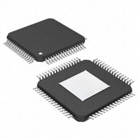
64-PIN, HTQFP PACKAGE (TOP VIEW)
PGND_AB
PGND_AB
OUT_B
OUT_B
PVDD_B
PVDD_B
BST_B
BST_C
PVDD_C
PVDD_C
OUT_C
OUT_C
PGND_CD
PGND_CD
OUT_D
OUT_A
PAP Package
(Top View)
64 63 62 61 60 59 58 57 56 55 54 53 52 51 50 49
OUT_A
PVDD_A
PVDD_A
BST_A
GVDD_AB
VDD
TEST1
OC_ADJ
FAULT
AVDD
AVSS
PLL_FLTM
PLL_FLTP
VR_ANA
DVDD
RESET
1
2
3
4
5
6
48
47
46
45
44
43
OUT_D
PVDD_D
PVDD_D
BST_D
GVDD_CD
7
8
9
10
11
12
13
14
15
16
42
41
40
39
38
37
36
35
34
33
GND
GND
SUB_PWM+
SUB_PWM–
VALID
BKND_ERR
VREG
MCLK
DVDD
CONFIG_1
CONFIG_2
GAIN_1
GAIN_0
FORMAT2
FORMAT1
FORMAT0
MUTE
LRCLK
SCLK
SDIN2
SDIN1
DVSS
VR_DIG
DVSSO
PDN
VREG_EN
OSC_RES
17 18 19 20 21 22 23 24 25 26 27 28 29 30 31 32
P0071-03
PIN FUNCTIONS
PIN
NAME
NO.
I/O (1)
5-V
TOLERANT
TERMINATION
DESCRIPTION
(2) (3)
AVDD
10
AVSS
11
P
BKND_ERR
37
DI
BST_A
4
P
High-side bootstrap supply for half-bridge A
BST_B
57
P
High-side bootstrap supply for half-bridge B
BST_C
56
P
High-side bootstrap supply for half-bridge C
(1)
(2)
(3)
P
3.3-V Analog power supply
Analog 3.3-V supply ground
Pullup
Active low. A back-end error sequence is initiated by applying a logic
low to this pin. Connect to an external power stage. If no external
power stage is used, connect directly to DVDD.
TYPE: A = analog; D = 3.3-V digital; P = power/ground/decoupling; I = input; O = output
All pullups are 20-mA weak pullups and all pulldowns are 20-mA weak pulldowns. The pullups and pulldowns are included to assure
proper input logic levels if the terminals are left unconnected (pullups → logic 1 input; pulldowns → logic 0 input). Devices that drive
inputs with pullups must be able to sink 50 mA while maintaining a logic-0 drive level. Devices that drive inputs with pulldowns must be
able to source 50 mA while maintaining a logic-1 drive level.
If desired, low-ESR capacitance values can be implemented by paralleling two or more ceramic capacitors of equal value. Paralleling
capacitors of equal value provides an extended high-frequency supply decoupling. This approach avoids the potential of producing
parallel resonance circuits that have been observed when paralleling capacitors of different values.
Submit Documentation Feedback
Copyright © 2008–2010, Texas Instruments Incorporated
Product Folder Link(s): TAS5701
5
�TAS5701
SLOS559A – JUNE 2008 – REVISED AUGUST 2010
www.ti.com
PIN FUNCTIONS (continued)
PIN
NAME
NO.
I/O (1)
5-V
TOLERANT
TERMINATION
DESCRIPTION
(2) (3)
BST_D
45
P
CONFIG_2
33
P
Pulldown
Input/output configuration. Connect this terminal directly to GND.
CONFIG_1
34
P
Pulldown
Input/output configuration. Connect this terminal directly to DVDD.
DVDD
15, 35
P
3.3-V Digital power supply
DVSS
26
P
Digital ground
DVSSO
20
P
Oscillator ground
FAULT
9
DO
FORMAT2
30
DI
Pulldown
Digital data format select MSB.
FORMAT1
31
DI
Pulldown
Digital data format select LSB.
FORMAT0
32
DI
Pulldown
Digital data format select.
GAIN_1
28
DI
5-V
MSB of gain select.
GAIN_0
29
DI
5-V
LSB of gain select. GAIN_0 and GAIN_1 allow 4 possible gain
selections.
GND
High-side bootstrap supply for half-bridge D
Overtemperature, undervoltage, and overcurrent fault reporting.
Active low indicates fault. If high, normal operation.
41, 42
P
Analog ground for power stage.
GVDD_AB
5
P
Gate drive voltage for half-bridges A and B (10.8 V to 13.2 V)
GVDD_CD
44
P
Gate drive voltage for half-bridges C and D (10.8 V to 13.2 V)
LRCLK
22
DI
5-V
Input serial audio data left/right clock (sampling rate clock)
MCLK
36
DI
5-V
Clock master input. The input frequency of this clock can range from
4.9 MHz to 49 MHz.
MUTE
21
DI
5-V
OC_ADJ
8
AO
Analog overcurrent programming. Requires 22-kΩ resistor to ground.
OSC_RES
19
AO
Oscillator trim resistor. Connect an 18.2-kΩ (1% tolerance is
required) resistor to DVSSO.
OUT_A
1, 64
O
Output, half-bridge A
OUT_B
60, 61
O
Output, half-bridge B
OUT_C
52, 53
O
Output, half-bridge C
OUT_D
48, 49
O
17
DI
PGND_AB
62, 63
P
Power ground for half-bridges A and B
PGND_CD
50, 51
P
Power ground for half-bridges C and D
PLL_FLTM
12
AO
PLL negative loop filter terminal
PLL_FLTP
13
AI
PLL positive loop filter terminal
PVDD_A
2, 3
P
Power supply input for half-bridge output A (0 V–21 V)
PVDD_B
58, 59
P
Power supply input for half-bridge output B (0 V–21 V)
PVDD_C
54, 55
P
Power supply input for half-bridge output C (0 V–21 V)
PVDD_D
46, 47
P
Power supply input for half-bridge output D(0 V–21 V)
16
DI
PDN
RESET
6
Pullup
Performs a soft mute of outputs, active-low. A logic low on this pin
sets the outputs equal to 50% duty cycle. A logic high on this pin
allows normal operation. The mute control provides a noiseless
volume ramp to silence. Releasing mute provides a noiseless ramp to
previous volume.
Output, half-bridge D
5-V
5-V
Pullup
Pullup
Power down, active-low. PDN stops all clocks, and outputs stop
switching whenever a logic low is applied. When PDN is released, the
device powers up all logic, starts all clocks, and performs a soft start
that returns to the previous configuration changes to FORMATx and
GAINx pins are ignored on PDN cycling.
Reset, active-low. A system reset is generated by applying a logic
low to this terminal. RESET is an asynchronous control signal that
sets the VALID outputs low, and places the PWM in the hard mute
state (stop switching). Gain is immediately set to full attenuation.
Upon the release of RESET, if PDN is high, the system performs a
4-ms to 5-ms device initialization and sets the gain and format to the
settings determined by the hardware pins.
Submit Documentation Feedback
Copyright © 2008–2010, Texas Instruments Incorporated
Product Folder Link(s): TAS5701
�TAS5701
www.ti.com
SLOS559A – JUNE 2008 – REVISED AUGUST 2010
PIN FUNCTIONS (continued)
PIN
NAME
NO.
I/O (1)
5-V
TOLERANT
TERMINATION
DESCRIPTION
(2) (3)
SCLK
23
DI
5-V
Serial audio data clock (shift clock). SCLK is the serial audio port
input data bit clock.
SDIN1
25
DI
5-V
Serial audio data 1 input is one of the serial data input ports. SDIN1
supports three discrete (stereo) data formats.
SDIN2
24
DI
5-V
Serial audio data 2 input is one of the serial data input ports. SDIN2
supports three discrete (stereo) data formats.
SUB_PWM–
39
DO
Subwoofer negative PWM output. BD modulated signal.
SUB_PWM+
40
DO
Subwoofer positive PWM output. BD modulated signal.
TEST1
7
DI
Test pin. Connect directly to GND.
VALID
38
DO
Output indicating validity of ALL PWM channels, active-high. This pin
is connected to an external power stage. If no external power stage is
used, leave this pin floating.
VDD
6
P
Power supply for VREG (10.8 V to 13.2 V)
VR_ANA
14
P
Internally regulated 1.8-V analog supply voltage. This terminal must
not be used to power external devices.
VR_DIG
27
P
Internally regulated 1.8-V analog supply voltage. This terminal must
not be used to power external devices.
VREG
43
P
VREG_EN
18
DI
Digital regulator output. Not to be used for powering external circuitry.
Pulldown
Voltage regulator enable. Connect directly to GND.
ABSOLUTE MAXIMUM RATINGS
over operating free-air temperature range (unless otherwise noted)
(1)
VALUE
GVDD, VDD
Supply voltage
Input voltage
PVDD
–0.3 to 23
DVDD
–0.3 to 3.6
AVDD
–0.3 to 3.6
OUT_X to GND_X
–0.3 to 30
BST_X to GND_X
–0.3 to 43.2
3.3-V digital input
–0.5 to DVDD + 0.5
5-V tolerant
(2)
UNIT
–0.3 to 13.2
digital input
–0.5 to DVDD + 2.5
V
V
Input clamp current, IIK (VI < 0 or VI > 1.8 V)
±20
mA
Output clamp current, IOK (VO < 0 or VO > 1.8 V)
±20
mA
0 to 85
°C
0 to 150
°C
–40 to 125
°C
Operating free-air temperature
Operating junction temperature range
Storage temperature range, Tstg
(1)
(2)
Stresses beyond those listed under absolute ratings may cause permanent damage to the device. These are stress ratings only and
functional operation of the device at these or any other conditions beyond those indicated under recommended operation conditions are
not implied. Exposure to absolute-maximum conditions for extended periods may affect device reliability.
5-V tolerant inputs are PDN, RESET, MUTE, SCLK, LRCLK, MCLK, SDIN1, SDIN2.
Submit Documentation Feedback
Copyright © 2008–2010, Texas Instruments Incorporated
Product Folder Link(s): TAS5701
7
�TAS5701
SLOS559A – JUNE 2008 – REVISED AUGUST 2010
www.ti.com
THERMAL INFORMATION
TAS5701
THERMAL METRIC (1) (2)
qJA
Junction-to-ambient thermal resistance
qJCtop
Junction-to-case (top) thermal resistance
qJB
Junction-to-board thermal resistance
13
yJT
Junction-to-top characterization parameter
0.1
yJB
Junction-to-board characterization parameter
7.9
qJCbot
Junction-to-case (bottom) thermal resistance
0.9
(1)
(2)
UNITS
PAP (64 PINS)
27.2
16
°C/W
For more information about traditional and new thermal metrics, see the IC Package Thermal Metrics application report, SPRA953.
For thermal estimates of this device based on PCB copper area, see the TI PCB Thermal Calculator.
RECOMMENDED OPERATING CONDITIONS
over operating free-air temperature range (unless otherwise noted)
MIN
NOM
MAX
UNIT
10.8
12
13.2
V
21
V
Gate drive supply voltage
GVDD, VDD
Output bridge supply voltage
PVDD
0
Digita supply voltage
DVDD
3
3.3
3.6
V
3.3
3.6
V
Analog supply voltage
AVDD
3
VIH
High-level input voltage
3.3-V TTL, 5-V tolerant
2
VIL
Low-level input voltage
3.3-V TTL, 5-V tolerant
TA
Operating ambient temperature range
TJ
Operating junction temperature range
RL (BTL)
RL (SE)
Load impedance
Output filter: L = 22 mH, C = 680 nF.
RL (PBTL)
V
0.8
V
0
85
°C
0
150
°C
6.0
8
3.2
4
3.2
LO (BTL)
Ω
4
10
LO (SE)
Minimum output inductance under
short-circuit condition
Output-filter inductance
10
LO (PBTL)
mH
10
PWM OPERATION AT RECOMMENDED OPERATING CONDITIONS
PARAMETER
Output sample rate 2×–1×
oversampled
TEST CONDITIONS
MODE
VALUE
UNIT
384
kHz
8×, 4×, and 2× sample rates
352.8
kHz
8×, 4×, and 2× sample rates
384
kHz
32–kHz data rate ±2%
12× sample rate
44.1-, 88.2-, 176.4-kHz data rate ±2%
48-, 96-, 192-kHz data rate ±2%
PLL INPUT PARAMETERS AND EXTERNAL FILTER COMPONENTS
PARAMETER
fMCLKI
TEST CONDITIONS
MIN
Frequency, MCLK (1 / tcyc2)
TYP
MAX
UNIT
49.2
MHz
50%
60%
4.9
MCLK duty cycle
40%
MCLK minimum high time
≥2-V MCLK = 49.152 MHz, within the
min and max duty cycle constraints
8
ns
MCLK minimum low time
≤0.8-V MCLK = 49.152 MHz, within the
min and max duty cycle constraints
8
ns
LRCLK allowable drift before LRCLK reset
8
4
MCLKs
External PLL filter capacitor C1
SMD 0603 Y5V
47
nF
External PLL filter capacitor C2
SMD 0603 Y5V
4.7
nF
External PLL filter resistor R
SMD 0603, metal film
470
Ω
Submit Documentation Feedback
Copyright © 2008–2010, Texas Instruments Incorporated
Product Folder Link(s): TAS5701
�TAS5701
www.ti.com
SLOS559A – JUNE 2008 – REVISED AUGUST 2010
ELECTRICAL CHARACTERISTICS
DC Characteristics
TA = 25 °C, PVCC_X = 18 V, DVDD = AVDD = 3.3 V, RL = 8 Ω (unless otherwise noted)
PARAMETER
TEST CONDITIONS
MIN
TYP MAX
VOH
High-level output voltage
3.3-V TTL and 5-V tolerant
(1)
IOH = –4 mA
VOL
Low-level output voltage
3.3-V TTL and 5-V tolerant
(1)
IOL = 4 mA
0.5
VI = 0 V, DVDD = 3.6 V
±2
Low-level input current
LRCLK, SCLK, SDINx, MCLK,
GAIN_x, VREG_EN,
FORMATx, CONFIG_x
BKND_ERR, RESET, PDN,
MUTE
VI = 0 V, DVDD = 3.6 V
±50
RESET, PDN, MUTE, GAIN_x,
BKND_ERR
VI = 3.6 V, DVDD = 3.6 V
±2
VREG_EN, FORMAT_x,
CONFIG_x, LRCLK, SCLK,
SDINx, MCLK
VI = 3.6 V, DVDD = 3.6 V
±50
RESET, PDN, MUTE, LRCLK,
SCLK, SDINx, MCLK, GAIN_x
VI = 5.5 V, DVDD = 3.6 V
±50
IIL
IIH
High-level input current
2.4
Input digital supply current Supply voltage (DVDD, AVDD)
Power down (PDN = low)
Reset (RESET = low)
Normal mode, 50% duty cycle
Gate supply current per
GVDD_xx input
IGVDD
V
V
mA
Normal mode, 50% duty cycle
IDD
UNIT
65
80
8
16
23
33
5
10
RESET = 0
2.2
4
PDN = 0
2.2
4
mA
mA
mA
IPVDD
Input power supply current
No load
30
60
mA
IPVDD(PDN)
Power-down current
No load, PDN = 0
1
100
mA
IPVDD(RESET)
Reset current
No load, RESET = 0
1
100
mA
Drain-to-source
resistance, LS
TJ = 25°C, includes
metallization resistance
140
Drain-to-source
resistance, HS
TJ = 25°C, includes
metallization resistance
140
Vuvp
Undervoltage protection
limit
PVDD falling
9.2
V
Vuvp,hyst
Undervoltage protection
limit
PVDD rising
9.6
V
150
°C
30
°C
1.25
ms
4.5
A
150
ns
22
kΩ
3
kΩ
rDS(on)
mΩ
I/O Protection
OTE
(2)
OTEHYST
Overtemperature error
(2)
Extra temperature drop
required to recover from
error
OLPC
Overload protection
counter
fPWM = 384 kHz
IOC
Overcurrent limit
protection
ROCP = 22 kΩ
IOCT
Overcurrent response
time
ROCP
OC programming resistor
range
Resistor tolerance = 5% for
typical value; the minimum
resistance should not be less
than 20 kΩ.
RPD
Internal pulldown resistor
at the output of each
half-bridge
Connected when RESET is
active to provide bootstrap
capacitor charge.
(1)
(2)
20
5-V tolerant inputs are PDN, RESET, MUTE, SCLK, LRCLK, MCLK, SDIN1, SDIN2, GAIN_0, and GAIN_1.
Specified by design.
Submit Documentation Feedback
Copyright © 2008–2010, Texas Instruments Incorporated
Product Folder Link(s): TAS5701
9
�TAS5701
SLOS559A – JUNE 2008 – REVISED AUGUST 2010
www.ti.com
AC Characteristics (BTL)
PVDD_X = 18 V, BTL mode, RL = 8 Ω, ROC = 22 kΩ, CBST = 33-nF, audio frequency = 1 kHz, AES17 filter, FPWM = 384 kHz,
TA = 25°C (unless otherwise noted). All performance is I naccordance with recommended operating conditions, unless
otherwise specified.
PARAMETER
PO
TEST CONDITIONS
Power output per channel
20.0
PVDD = 18 V, 7% THD, 1-kHz input signal
18.6
PVDD = 12 V, 10% THD, 1-kHz input
signal
Vn
Total harmonic distortion + noise
SNR
Signal-to-noise ratio
PD
Power dissipation due to idle losses (IPVDD_X)
(1)
(2)
10
PVDD = 12 V, PO = 4.5 W (half-power)
0.08%
1W
0.05%
Crosstalk
UNIT
W
8.3
0.1%
A-weighted
MAX
9
PVDD = 18 V, PO = 10 W (half-power)
Output integrated noise
(1)
TYP
PVDD = 18 V, 10% THD, 1-kHz input
signal
PVDD = 12 V, 7% THD, 1-kHz input signal
THD+N
MIN
50
mV
PO = 1 W, f = 1 kHz
–73
dB
A-weighted, f = 1 kHz, maximum power at
THD < 1%
101
dB
PO = 0 W, 4 channels switching (2)
0.6
W
SNR is calculated relative to 0-dBFS input level.
Actual system idle losses are affected by core losses of output inductors.
Submit Documentation Feedback
Copyright © 2008–2010, Texas Instruments Incorporated
Product Folder Link(s): TAS5701
�TAS5701
www.ti.com
SLOS559A – JUNE 2008 – REVISED AUGUST 2010
SERIAL AUDIO PORTS SLAVE MODE
Serial audio ports slave mode over recommended operating conditions (unless otherwise noted)
TEST
CONDITIONS
PARAMETER
CL = 30 pF
MIN
TYP
1.024
MAX
UNIT
12.288
MHz
fSCLKIN
Frequency, SCLK 32 × fS, 48 × fS, 64 × fS
tsu1
Setup time, LRCLK to SCLK rising edge
10
ns
th1
Hold time, LRCLK from SCLK rising edge
10
ns
tsu2
Setup time, SDIN to SCLK rising edge
10
ns
th2
Hold time, SDIN from SCLK rising edge
10
LRCLK frequency
32
48
192
SCLK duty cycle
40%
50%
60%
LRCLK duty cycle
40%
50%
60%
32
64
SCLK
edges
–1/4
1/4
SCLK
period
SCLK rising edges between LRCLK rising edges
t(edge)
LRCLK clock edge with respect to the falling edge of SCLK
ns
kHz
SCLK
(Input)
t(edge)
th1
tsu1
LRCLK
(Input)
th2
tsu2
SDIN
T0026-03
Figure 2. Slave Mode Serial Data Interface Timing
HARDWARE SELECT PINS
over recommended operating conditions (unless otherwise noted)
PARAMETER
tsu
MIN
Setup time, FORMATx, CONFIG_x, GAIN_x to RESET rising edge
TYP
MAX
100
UNIT
ms
tsu
FORMATx,
CONFIG_x,
GAIN_x,
RESET
Figure 3. Mode Pins Setup Time
Submit Documentation Feedback
Copyright © 2008–2010, Texas Instruments Incorporated
Product Folder Link(s): TAS5701
11
�TAS5701
SLOS559A – JUNE 2008 – REVISED AUGUST 2010
www.ti.com
RESET TIMING (RESET) AND POWER-ON RESET
Control signal parameters over recommended operating conditions (unless otherwise noted)
PARAMETER
MIN
td(VALID_LOW)
Time to assert VALID (reset to power stage) low
tw(RESET)
Pulse duration, RESET active
td(START)
Time to start-up
100
RESET
TYP
MAX
UNIT
100
ns
200
ms
3.6
ms
Earliest time
that hard mute
could be exited
tw(RESET)
VALID
td(START)
Start system
td(VALID_LOW)
T0029-05
Figure 4. Reset Timing
When power is applied to DVDD, RESET must be held low for at least 100 ms after DVDD reaches 3.0 V.
3.6 V
3.0 V
DVDD
0V
RESET
100 ms
Figure 5. Power-On Reset Timing
POWER-DOWN (PDN) TIMING
Control signal parameters over recommended operating conditions (unless otherwise noted)
PARAMETER
MIN
TYP
MAX
UNIT
td(VALID_LOW)
Time to assert VALID (reset to power stage) low
725
ms
td(STARTUP)
Device start-up time
650
ms
tw
Minimum pulse duration required
1
ms
PDN
tw
VALID
td(VALID_LOW)
td(STARTUP)
T0030-04
Figure 6. Power-Down Timing
12
Submit Documentation Feedback
Copyright © 2008–2010, Texas Instruments Incorporated
Product Folder Link(s): TAS5701
�TAS5701
www.ti.com
SLOS559A – JUNE 2008 – REVISED AUGUST 2010
BACK-END ERROR (BKND_ERR)
Control signal parameters over recommended operating conditions (unless otherwise noted)
PARAMETER
MIN
TYP
tw(ER)
Pulse duration, BKND_ERR active (active-low)
tp(valid_high)
Time to stay in the OUT_x low state. After tp(valid_high), the TAS5701 attempts to bring
the system out of the OUT_x low state if BKND_ERR is high.
300
tp(valid_low)
Time TAS5701 takes to bring OUT_x low after BKND_ERR assertion.
350
MAX
UNIT
350
ns
ms
ns
tw(ER)
BKND_ERR
VALID
Normal
Operation
Normal
Operation
tp(valid_high)
tp(valid_low)
T0031-04
Figure 7. Error Recovery Timing
MUTE TIMING (MUTE)
Control signal parameters over recommended operating conditions (unless otherwise noted)
PARAMETER
td(VOL)
(1)
MIN
Volume ramp time. Ramp time = Number of steps × stepsize
(1)
TYP
MAX
1024
UNIT
steps
Stepsize = 4 LRCLKs (for 32–48 kHz sample rate); 8 LRCLKs (for 88.2–96 kHz sample rate); 16 LRCLKs (for 176.4–192 kHz sample
rate)
MUTE
VOLUME
Normal
Operation
Normal
Operation
td(VOL)
td(VOL)
50-50
Duty Cycle
T0032-03
Figure 8. Mute Timing
Submit Documentation Feedback
Copyright © 2008–2010, Texas Instruments Incorporated
Product Folder Link(s): TAS5701
13
�TAS5701
SLOS559A – JUNE 2008 – REVISED AUGUST 2010
www.ti.com
TYPICAL CHARACTERISTICS, BTL CONFIGURATION
TOTAL HARMONIC DISTORTION + NOISE
vs
OUTPUT POWER
TOTAL HARMONIC DISTORTION + NOISE
vs
OUTPUT POWER
10
THD+N - Total Harmonic Distortion + Noise - %
THD+N - Total Harmonic Distortion + Noise - %
10
PVDD = 18 V
RL = 8 W
1
10 kHz
1 kHz
0.1
0.01
20 Hz
0.001
0.01
0.1
1
10
PO - Output Power - W
10 kHz
1 kHz
0.1
0.01
20 Hz
0.1
1
10
PO - Output Power - W
Figure 10.
TOTAL HARMONIC DISTORTION + NOISE
vs
FREQUENCY
TOTAL HARMONIC DISTORTION + NOISE
vs
FREQUENCY
10
PVDD = 18 V
RL = 8 Ω
1
P=5W
0.1
0.01
P = 0.5 W
P = 2.5 W
100
1k
10k 20k
PVDD = 18 V
RL = 6 Ω
1
P=5W
0.1
0.01
P = 2.5 W
0.001
20
f − Frequency − Hz
100
P = 0.5 W
1k
10k 20k
f − Frequency − Hz
G001
Figure 11.
14
100
Figure 9.
THD+N − Total Harmonic Distortion + Noise − %
THD+N − Total Harmonic Distortion + Noise − %
1
0.001
0.01
100
10
0.001
20
PVDD = 18 V
RL = 6 W
G002
Figure 12.
Submit Documentation Feedback
Copyright © 2008–2010, Texas Instruments Incorporated
Product Folder Link(s): TAS5701
�TAS5701
www.ti.com
SLOS559A – JUNE 2008 – REVISED AUGUST 2010
TYPICAL CHARACTERISTICS, BTL CONFIGURATION (continued)
SYSTEM EFFICIENCY
vs
OUTPUT POWER
SUPPLY CURRENT
vs
OUTPUT POWER
3.0
100
PVDD = 18 V
90
RL = 6 Ω
2.5
80
Efficiency − %
ICC − Supply Current − A
RL = 6 Ω
70
RL = 8 Ω
60
50
40
30
20
1.5
RL = 8 Ω
1.0
0.5
10
PVDD = 18 V
0.0
0
0
4
8
12
16
0
20
10
20
30
40
50
PO − Output Power − W
PO − Output Power (Per Channel) − W
G006
G005
Figure 13.
Figure 14.
OUTPUT POWER
vs
SUPPLY VOLTAGE
OUTPUT POWER
vs
SUPPLY VOLTAGE
40
40
RL = 8 Ω
35
RL = 6 Ω
35
30
PO − Output Power − W
30
PO − Output Power − W
2.0
25
20
THD+N = 10%
15
THD+N = 1%
10
25
THD+N = 10%
20
15
THD+N = 1%
10
5
5
0
0
10
11
12
13
14
15
16
17
18
19
20
21
10
11
PVDD − Supply Voltage − V
12
13
14
15
16
17
18
19
20
21
PVDD − Supply Voltage − V
G007
Figure 15.
G008
Figure 16.
Submit Documentation Feedback
Copyright © 2008–2010, Texas Instruments Incorporated
Product Folder Link(s): TAS5701
15
�TAS5701
SLOS559A – JUNE 2008 – REVISED AUGUST 2010
www.ti.com
TYPICAL CHARACTERISTICS, BTL CONFIGURATION (continued)
CROSSTALK
vs
FREQUENCY
−40
−50
PVDD = 18 V
RL = 8 Ω
−60
Crosstalk − dB
−70
Left to Right
−80
Right to Left
−90
−100
−110
−120
20
100
1k
10k 20k
f − Frequency − Hz
G010
Figure 17.
DETAILED DESCRIPTION
POWER SUPPLY
The digital portion of the chip requires 3.3 V, and the analog portion can work with a variable range up to 12 V.
PVDD has a maximum operational range up to 22 V.
To facilitate system design, the TAS5701 needs only a 12-V supply in addition to the (typical) 18-V power-stage
supply. An internal voltage regulator provides suitable voltage levels for the digital and low-voltage analog
circuitry. Additionally, all circuitry requiring a floating voltage supply, e.g., the high-side gate drive, is
accommodated by built-in bootstrap circuitry requiring only a few external capacitors.
In order to provide outstanding electrical and acoustical characteristics, the PWM signal path including gate drive
and output stage is designed as identical, independent half-bridges. For this reason, each half-bridge has
separate gate drive supply (GVDD_X), bootstrap pins (BST_X), and power-stage supply pins (PVDD_X). Special
attention should be paid to placing all decoupling capacitors as close to their associated pins as possible. In
general, inductance between the power supply pins and decoupling capacitors must be avoided.
For a properly functioning bootstrap circuit, a small ceramic capacitor must be connected from each bootstrap pin
(BST_X) to the power-stage output pin (OUT_X). When the power-stage output is low, the bootstrap capacitor is
charged through an internal diode connected between the gate-drive power-supply pin (GVDD_X) and the
bootstrap pin. When the power-stage output is high, the bootstrap capacitor potential is shifted above the output
potential and thus provides a suitable voltage supply for the high-side gate driver. In an application with PWM
switching frequencies in the range from 352 kHz to 384 kHz, it is recommended to use 33-nF ceramic capacitors,
size 0603 or 0805, for the bootstrap supply. These 33-nF capacitors ensure sufficient energy storage, even
during minimal PWM duty cycles, to keep the high-side power stage FET (LDMOS) fully turned on during the
remaining part of the PWM cycle. In an application running at a reduced switching frequency, generally 192 kHz,
the bootstrap capacitor might need to be increased in value.
Special attention should be paid to the power-stage power supply; this includes component selection, PCB
placement, and routing. As indicated, each half-bridge has independent power-stage supply pins (PVDD_X). For
optimal electrical performance, EMI compliance, and system reliability, it is important that each PVDD_X pin is
decoupled with a 100-nF ceramic capacitor placed as close as possible to each supply pin.
16
Submit Documentation Feedback
Copyright © 2008–2010, Texas Instruments Incorporated
Product Folder Link(s): TAS5701
�TAS5701
www.ti.com
SLOS559A – JUNE 2008 – REVISED AUGUST 2010
The 12-V supply should be from a low-noise, low-output-impedance voltage regulator. Likewise, the 18-V
power-stage supply is assumed to have low output impedance and low noise. The power-supply sequence is not
critical as facilitated by the internal power-on-reset circuit. Moreover, the TAS5701 is fully protected against
erroneous power-stage turnon due to parasitic gate charging.
Clock, Auto Detection, and PLL
The TAS5701 digital audio processor (DAP) is a clock slave device. It accepts MCLK, SCLK, and LRCLK.
The TAS5701 checks to verify that SCLK is a specific value of 32-fs, 48- fs, or 64-fs. The DAP only supports a 1 ×
fs LRCLK. The timing relationship of these clocks to SDIN1and SIN2 is shown in subsequent sections. The clock
section uses MCLK or the internal oscillator clock (when MCLK is unstable or absent) to produce the internal
clock.
The DAP can auto-detect and set the internal clock control logic to the appropriate settings for the frequencies of
32 kHz, normal speed (44.1 or 48 kHz), double speed (88.2 kHz or 96 kHz), and quad speed (176.4 kHz or 192
kHz).
SERIAL DATA INTERFACE
Serial data is input on SDIN1 and SIN2. The PWM outputs are derived from SDIN1 ands SIN2. The TAS5701
DAP accepts 32-, 44.1-, 48-, 88.2-, 96-, 176.4-, and 192-kHz serial data in 16-, 18-, 20-, or 24-bit data in
left-justified, right-justified, and I2S serial data formats. See Table 1 for format control settings.
SDIN1 left channel data is sent to OUTA/OUTB configured in BTL. SDIN1 right channel data is sent to
OUTC/OUTD. SDIN2 left channel data is sent to SUB_PWM+/–. The right channel data of SDIN2 is ignored.
PWM SECTION
The DAP (digital audio processor) has three channels of high-performance digital PWM modulators that are
designed to drive bride-tied output H-bridge configurations with BD modulation.
The DAP uses noise-shaping and sophisticated error correction algorithms to achieve high power efficiency and
high-performance digital audio reproduction. The DAP uses a fourth-order noise shaper to provide >100-dB SNR
performance from 20 Hz to 20 kHz.
The PWM section accepts 24-bit PCM data from the DAP and outputs three PWM audio output channels. The
PWM section output supports bridge-tied loads ONLY.
The PWM section has individual channel dc blocking filters that are ALWAYS enabled. The filter cutoff frequency
is less than 1 Hz.
Finally, the PWM section has a fixed maximum modulation limit of 97.7%.
SERIAL INTERFACE CONTROL AND TIMING
I2S Timing
I2S timing uses LRCLK to define when the data being transmitted is for the left channel and when it is for the
right channel. LRCLK is low for the left channel and high for the right channel. A system clock (SCLK) running at
32, 48, or 64 × fs is used to clock in the data. There is a delay of one bit clock from the time the LRCLK signal
changes state to the first bit of data on the data lines. The data is written MSB first and is valid on the rising edge
of the bit clock. The DAP masks unused trailing data bit positions.
Submit Documentation Feedback
Copyright © 2008–2010, Texas Instruments Incorporated
Product Folder Link(s): TAS5701
17
�TAS5701
SLOS559A – JUNE 2008 – REVISED AUGUST 2010
www.ti.com
1/fS
LRCK
L-Channel
R-Channel
SCLK
(= 32 fS, 48 fS or 64 fS)
DATA
2
N−1 N−2 N−3
1
0
N–1
LSB
MSB
2
N–2 N–3
1
0
N−1
N−2
LSB
MSB
Figure 18. I2S Format
Left-Justified
Left-justified (LJ) timing uses LRCLK to define when the data being transmitted is for the left channel and when it
is for the right channel. LRCLK is high for the left channel and low for the right channel. A bit clock running at 32,
48, or 64 × fs is used to clock in the data. The first bit of data appears on the data lines at the same time LRCLK
toggles. The data is written MSB first and is valid on the rising edge of the bit clock. The DAP masks unused
trailing data bit positions.
1/fS
LRCK
L-Channel
R-Channel
SLCK
(= 32 fS, 48 fS, or 64 fS)
DATA
N−1 N−2 N−3
MSB
2
1
LSB
0
N−1 N−2
2
N−3
MSB
1
0
N–1
N–2
LSB
Figure 19. Left-Justified Format
Right-Justified
Right-justified (RJ) timing uses LRCLK to define when the data being transmitted is for the left channel and when
it is for the right channel. LRCLK is high for the left channel and low for the right channel. A bit clock running at
32, 48, or 64 × fs is used to clock in the data. The first bit of data appears on the data 8 bit-clock periods (for
24-bit data) after LRCLK toggles. In RJ mode the LSB of data is always clocked by the last bit clock before
LRCLK transitions. The data is written MSB first and is valid on the rising edge of the bit clock. The DAP masks
unused leading data bit positions.
18
Submit Documentation Feedback
Copyright © 2008–2010, Texas Instruments Incorporated
Product Folder Link(s): TAS5701
�TAS5701
www.ti.com
SLOS559A – JUNE 2008 – REVISED AUGUST 2010
1/fS
LRCK
L-Channel
R-Channel
SCLK
(= 32 fS, 48 fS, or 64 fS)
16-Bit Right-Justified, SCLK = 48 fS or 64 fS
DATA
2
1
0
15 14 13
2
MSB
1
0
15 14 13
2
1
MSB
LSB
0
LSB
16-Bit Right-Justified, SCLK = 32 fS
DATA
2
1
0
15 14 13
2
1
0
15 14 13
MSB
LSB
MSB
2
1
0
LSB
18-Bit Right-Justified, SCLK = 48 fS or 64 fS
DATA
2
1
0
17 16 15
2
MSB
1
0
17 16 15
LSB
2
MSB
1
0
LSB
20-Bit Right-Justified, SCLK = 48 fS or 64 fS
DATA
2
1
0
19 18 17
2
MSB
1
0
19 18 17
LSB
2
MSB
1
0
LSB
24-Bit Right-Justified, SCLK = 48 fS
DATA
2
1
0
23 22 21
2
1
0
23 22 21
LSB
MSB
2
MSB
1
0
LSB
24-Bit Right-Justified, SCLK = 64 fS
DATA
2
1
0
23 22 21
MSB
2
1
0
23 22 21
2
MSB
LSB
1
0
LSB
Figure 20. Right-Justified Format
Format Control
The digital data input format is selected via three external terminals (FORMAT0, FORMAT1, and FORMAT2).
Table 1 lists the corresponding data format for SDIN1 and SDIN2. LRCLK and SCLK are shared clocks for
SDIN1 and SDIN2. Changes to the FORMATx terminals are latched in immediately on a rising edge of RESET.
Changes to the FORMATx terminals while RESET is high are not allowed.
Table 1. Format Control
SERIAL DIGITAL DATA
FORMAT
FORMAT2
FORMAT1
FORMAT0
0
0
0
16-Bit right-justifed
0
0
1
18-Bit right-justified
0
1
0
20-Bit right-justified
0
1
1
24-Bit right-justified
1
0
0
16-, 24-Bit I2S
1
0
1
16-, 24-Bit left-justified
1
1
0
Reserved. Setting is not allowed.
1
1
1
Reserved. Setting is not allowed.
Gain Control
The gain of the DAP is selected via two external gain pins (GAIN_0 and GAIN_1). Table 2 lists the corresponding
channel gain (for ALL channels) for GAIN_0 and GAIN_1 settings. Individual channel gain is not possible.
Changes to the GAIN_x terminals are latched in immediately on a rising edge of RESET. Changes to the
GAIN_x terminals while RESET is high are not allowed.
Submit Documentation Feedback
Copyright © 2008–2010, Texas Instruments Incorporated
Product Folder Link(s): TAS5701
19
�TAS5701
SLOS559A – JUNE 2008 – REVISED AUGUST 2010
www.ti.com
Table 2. Gain Control
GAIN_1
GAIN_0
CHANNEL GAIN (dB)
0
0
0
0
1
6
1
0
12
1
1
18
DEVICE PROTECTION SYSTEM
The TAS5701 contains advanced protection circuitry carefully designed to facilitate system integration and ease
of use, as well as to safeguard the device from permanent failure due to a wide range of fault conditions such as
short circuits, overtemperature, and undervoltage. The TAS5701 responds to a fault by immediately setting the
power stage in a high-impedance (Hi-Z) state and reporting the error on the FAULT pin (FAULT = 0); the device
automatically recovers when the fault condition has been removed.
Short-Circuit Protection
The device has independent, fast-reacting current detectors on all high-side and low-side power-stage FETs. The
detector outputs are closely monitored by a protection system. If a high-current condition situation exists, i.e., the
power stage outputs are shorted, the protection system triggers a latching shutdown, resulting in the power stage
being set in the high-impedance (Hi-Z) state and FAULT going low. Overcurrent protection is not independent for
half-bridges A and B and, respectively, C and D. That is, if the bridge-tied load between half-bridges A and B
causes an overcurrent fault, half-bridges A, B, C, and D are shut down.
Overtemperature Protection
If the device junction temperature exceeds 150°C (nominal), the device is put into thermal shutdown, resulting in
all half-bridge outputs being set in the high-impedance (Hi-Z) state and FAULT going low. Once the temperature
decreases 30°C (typical), the device resumes normal operation.
Undervoltage Protection (UVP) and Power-On Reset (POR)
The UVP and POR circuits of the TAS5701 fully protect the device in any power-up/down and brownout situation.
While powering up, the POR circuit resets the protection circuitry and ensures that all circuits are fully operational
when the VDD and GVDD_X supply voltages reach 9.6 V (typical). Although GVDD_x and VDD pins are
independently monitored, a supply voltage drop below the UVP threshold on any VDD or GVDD_x pin results in
all outputs immediately being set in the high-impedence (Hi-Z) state and FAULT pin being asserted low. The
device automatically resumes operation when all supply voltages have increased above the UVP threshold.
Spacer
REVISION HISTORY
Changes from Original (June 2008) to Revision A
•
20
Page
Replaced the with the DISSIPATION RATINGS table Thermal Information table ............................................................... 8
Submit Documentation Feedback
Copyright © 2008–2010, Texas Instruments Incorporated
Product Folder Link(s): TAS5701
�PACKAGE OPTION ADDENDUM
www.ti.com
14-Oct-2022
PACKAGING INFORMATION
Orderable Device
Status
(1)
Package Type Package Pins Package
Drawing
Qty
Eco Plan
(2)
Lead finish/
Ball material
MSL Peak Temp
Op Temp (°C)
Device Marking
(3)
Samples
(4/5)
(6)
TAS5701PAP
ACTIVE
HTQFP
PAP
64
160
RoHS & Green
NIPDAU
Level-3-260C-168 HR
TAS5701PAP-P
ACTIVE
HTQFP
PAP
64
160
RoHS & Green
NIPDAU
Level-3-260C-168 HR
TAS5701PAPR
ACTIVE
HTQFP
PAP
64
1000
RoHS & Green
NIPDAU
Level-3-260C-168 HR
0 to 85
0 to 85
TAS5701
Samples
TAS5701
Samples
TAS5701
Samples
(1)
The marketing status values are defined as follows:
ACTIVE: Product device recommended for new designs.
LIFEBUY: TI has announced that the device will be discontinued, and a lifetime-buy period is in effect.
NRND: Not recommended for new designs. Device is in production to support existing customers, but TI does not recommend using this part in a new design.
PREVIEW: Device has been announced but is not in production. Samples may or may not be available.
OBSOLETE: TI has discontinued the production of the device.
(2)
RoHS: TI defines "RoHS" to mean semiconductor products that are compliant with the current EU RoHS requirements for all 10 RoHS substances, including the requirement that RoHS substance
do not exceed 0.1% by weight in homogeneous materials. Where designed to be soldered at high temperatures, "RoHS" products are suitable for use in specified lead-free processes. TI may
reference these types of products as "Pb-Free".
RoHS Exempt: TI defines "RoHS Exempt" to mean products that contain lead but are compliant with EU RoHS pursuant to a specific EU RoHS exemption.
Green: TI defines "Green" to mean the content of Chlorine (Cl) and Bromine (Br) based flame retardants meet JS709B low halogen requirements of