User's Guide
SLOU331A – December 2011 – Revised August 2014
TAS5731EVM Evaluation Module
This manual describes the operation of the TAS5731EVM to evaluate the performance of the TAS5731
integrated digital audio power amplifier. The main contents of this document are:
• Details on how to properly connect a TAS5731 Evaluation Module (EVM) and the details of the EVM.
• Details on how to install and use the GUI to program the TAS5731EVM.
• Quick-start guide for the common modes in which the TAS5731EVM can be used.
• Details on how to use the audio processing features like EQ and DRC.
1
2
3
4
5
Contents
Overview ...................................................................................................................... 2
1.1
TAS5731EVM and MC57xxPSIA Features...................................................................... 3
Installation .................................................................................................................... 4
2.1
EVM Installation ..................................................................................................... 4
2.2
Software Installation ................................................................................................ 7
Using the GUI Software ..................................................................................................... 8
3.1
Setting the PPSI2C Environment Variable ...................................................................... 9
3.2
Launching the GUI interface ..................................................................................... 10
3.3
Initializing the Device ............................................................................................. 11
3.4
Using EQ Function ................................................................................................ 13
3.5
Using the DRC Function: ......................................................................................... 14
3.6
Using the Mixer and Scaler Nodes.............................................................................. 16
3.7
Using I2C Memory Tool .......................................................................................... 16
Jumpers and Control Utilities on MC57xxPSIA board ................................................................. 18
4.1
RCA/OPTICAL Jumpers .......................................................................................... 18
4.2
Switches ............................................................................................................ 18
4.3
LED Indicators ..................................................................................................... 18
Board Layouts, Schematic, and Bill of Materials ....................................................................... 19
5.1
TAS5731EVM Board Layouts ................................................................................... 19
5.2
TAS57xx PSIA Board Layout .................................................................................... 19
5.3
TAS5731EVM Schematic ........................................................................................ 20
5.4
Bill of Materials .................................................................................................... 21
List of Figures
1
TAS5731EVM Printed-Circuit Board ...................................................................................... 2
2
Complete System and EVM Signal Path Overview ..................................................................... 3
3
General Connection Picture ................................................................................................ 4
4
Connecting TAS5731EVM to MC57xxPSIA .............................................................................. 5
5
BTL Connection .............................................................................................................. 6
6
SE Connection ............................................................................................................... 6
7
TAS5731 DAP Block Diagram ............................................................................................. 8
8
System Properties Window ................................................................................................. 9
9
Environment Variable and User Variable Window ..................................................................... 10
10
Default GUI Interface on Start-up ........................................................................................ 11
11
Zoomed-In Snapshot of the Configuration Drop-Down Menu ........................................................ 11
12
Initiating Connect from the Target Menu ................................................................................ 12
SLOU331A – December 2011 – Revised August 2014
Submit Documentation Feedback
Copyright © 2011–2014, Texas Instruments Incorporated
TAS5731EVM Evaluation Module
1
�Overview
www.ti.com
13
Toggling Shut-Down and Mute States ................................................................................... 12
14
TAS57xx GUI EQ Blocks .................................................................................................. 13
15
EQ-Tool Filter Creation Window.......................................................................................... 14
16
TAS57X1 GUI DRC Blocks ............................................................................................... 14
17
TAS57xx GUI DRC Customization Tool ................................................................................. 15
18
DRC Time Constants Window ............................................................................................ 15
19
Input, Output Mixer and Scaler Nodes
20
I2C Memory Tool ........................................................................................................... 17
21
TAS5731EVM Top Composite Assembly ............................................................................... 19
22
TAS57xxPSIA Top Composite Assembly ............................................................................... 19
23
TAS5731EVM Schematic ................................................................................................. 20
..................................................................................
16
List of Tables
1
1
TAS5731EVM Bill Of materials (BOM) .................................................................................. 21
Overview
The TAS5731 evaluation module demonstrates the TAS5731 device from Texas Instruments. The
TAS5731 combines a high-performance PWM processor with a class-D audio power amplifier. This EVM
can be configured with two single-ended speakers with a BTL subwoofers (2.1) or two bridge-tied
speakers (BTL) (2.0). For detailed information about the TAS5731 device, review the device data sheet on
TI’s webpage. The TAS5731 has additional audio processing features such as surround sound (3D).
The EVM software with its graphic user interface (GUI) facilitates evaluation by providing access to the
TAS5731 registers through a USB port.
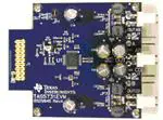
Figure 1. TAS5731EVM Printed-Circuit Board
2
TAS5731EVM Evaluation Module
SLOU331A – December 2011 – Revised August 2014
Submit Documentation Feedback
Copyright © 2011–2014, Texas Instruments Incorporated
�Overview
www.ti.com
The EVM, together with other TI components on this board, is a complete 2.1-channel digital audio
amplifier system. The MC57XXPSIA Controller board includes a USB interface, a digital input (SPDIF),
analog inputs via the ADC, power inputs, and other features like a mute function and power down
Left
MC57xxPSIA
TAS5731EVM
PC Interface
Right
SPDIF/
Optical, Coax
TAS5731
2CH Analog Input
From Other Source/
Digital Out
Subwoofer
Figure 2. Complete System and EVM Signal Path Overview
1.1
TAS5731EVM and MC57xxPSIA Features
•
•
•
•
•
•
•
•
Channel evaluation module design
Self-contained protection systems and control pins
USB interface
Standard I2S data input using optical or coaxial inputs
Analog input through analog-to-digital converter
Subwoofer connection—the PWM terminal provides the PWM signal and power to an external
subwoofer board
Double-sided, plated-through PCB, 1oz copper, 2mm
Access to control signal gain and data format through EVM-software GUI
SLOU331A – December 2011 – Revised August 2014
Submit Documentation Feedback
Copyright © 2011–2014, Texas Instruments Incorporated
TAS5731EVM Evaluation Module
3
�Installation
2
www.ti.com
Installation
This section describes the EVM and software installation.
2.1
EVM Installation
Figure 3. General Connection Picture
The following are the basic tools for the initial EVM power up.
• Power Supply for Digital Supply (5-V
• Power Supply (PVDD)
• Banana-plug test leads for power supplies and speakers
• Optical or coaxial cable for SPDIF interface based on signal source
• USB cable
• EVM software
• Speakers or Loads for outputs
The following sections describe the TAS5717LEVM board in regards to power supply (PSU) and system
interfaces.
4
TAS5731EVM Evaluation Module
SLOU331A – December 2011 – Revised August 2014
Submit Documentation Feedback
Copyright © 2011–2014, Texas Instruments Incorporated
�Installation
www.ti.com
2.1.1
Connecting the TAS5731EVM to MC57xxPSIA
On the right side of the MC57xxPSIA is a terminal block and another is located on the left of the
TAS5731EVM (labeled J1). Carefully place the MC57xxPSIA block above the TAS5731EVM block and
gently push down.
Figure 4. Connecting TAS5731EVM to MC57xxPSIA
2.1.2
PSU Interface
The TAS5731EVM is powered by two power supplies connected to the MC57xx controller board: a 5-V
power supply (VIN), and PVDD power supply. The 3.3-V level is generated on the board by a voltage
regulator from the 5-V supply.
NOTE: The power-supply cable length must be minimized. Increasing the length of the PSU cable
increases the distortion of the amplifier at high output levels and low frequencies.
The maximum output-stage supply voltage depends on the speaker load resistance. Check the
recommended maximum supply voltage in the TAS5731 data sheet (SLOS726).
2.1.3
Loudspeaker Connectors
CAUTION
All speaker outputs are biased at VCC/2 and must not be connected to ground
(e.g., through an oscilloscope ground).
Loudspeaker connections vary by device setup. When connecting a speaker in single-ended mode,
connect the positive terminal to one output on the TAS5731EVM (A, B, C, or D), and connect the negative
terminal to ground. When connecting a speaker in BTL mode, connect the speaker’s two terminals across
two outputs on the TAS5731EVM (A and B or C and D). Note that the EVM is setup to use only channels
A and B in the SE mode, for a real application; however, any of the channels can be setup for SE mode
operation.
Speakers or loads can be connected to the outputs A-D with clip leads, or cables can be made
with female connectors (JST VHR-2N) that can mate to male connectors on the EVM board.
SLOU331A – December 2011 – Revised August 2014
Submit Documentation Feedback
Copyright © 2011–2014, Texas Instruments Incorporated
TAS5731EVM Evaluation Module
5
�Installation
www.ti.com
+
OUT A
–
OUT B
Figure 5. BTL Connection
+
OUT A
–
Figure 6. SE Connection
2.1.4
USB Interface
The TAS5731 registers are accessed through I2C bus lines SDA and SCL. The USB circuit and USB
connector on the MC57xxPSIA board facilitates the connection between a host computer and the device.
The EVM USB circuit is powered by the 5V USB line of the host PC and is independent of the power
supplies available on the board. The USB device that is used is a TAS1020B from Texas Instruments.
2.1.5
Digital Audio Interface SPDIF
The Digital Audio Interface SPDIF (RCA/OPTO) accepts digital audio data using the I2S protocol. See the
TAS5731 data sheet for more information.
The RCA connector and the OPTO connector are the two SPDIF interfaces on the MC57xxPSIA board.
The jumper JP11 toggles between the OPTO and RCA connector to accommodate the signal source.
When the RCA cable or optical cable is connected and the signal source is powered up, verify that the
SPDIF lock indicator (blue LED5) illuminates, confirming that a viable signal is available to the device.
Install a jumper on JP4 across the middle pin and the pin marked SPDIF to connect the digital source to
SDIN1. Install a jumper on JP5 to connect the digital source to SDIN2.
For detailed information on how the data and clocks are provided to the TAS5717L, see the schematic
appearing at the end of this document and the DIR9001 device data sheet (SLES198).
2.1.6
ADC Interface
In the absence of a digital signal source, the PCM1808 ADC can be used to convert an analog audio
signal to a digital signal to the TAS5717L. The DIR9001 still provides clock signals to the ADC in this
process. A 12 MHz crystal is installed on the MC57xxPSIA board. The ADC is an additional feature of this
board to provide flexibility in sourcing an audio signal to the TAS5731. Review the PCM1808 data sheet
(SLES177) for a detailed description of the ADC on this EVM. Install the jumper on JP4 and J5 across the
middle pin and the pin marked ADC to select ADC as the source for SDIN1 and SDIN2, and finally, install
JP2 and JP3.
6
TAS5731EVM Evaluation Module
SLOU331A – December 2011 – Revised August 2014
Submit Documentation Feedback
Copyright © 2011–2014, Texas Instruments Incorporated
�Installation
www.ti.com
2.1.7
Board Power-Up General Guidelines
Connect the MC57xxPSIA and the TAS5717LEVM boards by locating pin 1 on each board, indicated by a
small white triangle. The MC57xxPSIA plugs down onto the TAS5731EVM board (that is, the
TAS5731EVM board fits underneath the MC57xxPSIA board). Pin 1 on each board must be connected to
each other.
Install the EVM software on the PC before powering up the board. After connecting the loudspeakers or
other loads, power supplies, and the data line, power up the 5-V power supply first; then power up the
PVDD power supply.
2.2
Software Installation
Download the TAS57X1 GDE from the TI Web site, located on the TAS5731EVM product page. The TI
Web site always has the latest release and any updates to versions of the GUI.
Execute the GUI install program, Setup.exe. Once the program is installed, the program group and
shortcut icon is created in Start → Program → Texas Instruments Inc → TAS57X1 GDE.
The TAS5717L tab opens when the GUI starts. The TAS5717L tab has two subwindows. One shows the
Process Flow window. This window also shows Input select, Mode select, Channel, and Master Volume.
All functions are shown in the same order as in the device.
The other subwindow, the Properties window, has the properties that a user can update by selecting from
the available options. The properties available depend on the device selected.
SLOU331A – December 2011 – Revised August 2014
Submit Documentation Feedback
Copyright © 2011–2014, Texas Instruments Incorporated
TAS5731EVM Evaluation Module
7
�Using the GUI Software
3
www.ti.com
Using the GUI Software
This section describes the details of using the TAS57xx Graphical User Interface (GUI) software tool to
interface with the TAS5731 device. The software is available for download at the TAS5731 product page
on www.ti.com. The main function of the GUI is to provide the user an easy way to manipulate the device
register space for attaining the required signal processing flow. The block diagram of the Digital Audio
Processing (DAP) flow of the TAS5731, taken from the TAS5731 data sheet is shown in Figure 7.
Figure 7. TAS5731 DAP Block Diagram
8
TAS5731EVM Evaluation Module
SLOU331A – December 2011 – Revised August 2014
Submit Documentation Feedback
Copyright © 2011–2014, Texas Instruments Incorporated
�Using the GUI Software
www.ti.com
3.1
Setting the PPSI2C Environment Variable
The I2C slave address of TAS5731 can either be 0x34 or 0x36 depending on the state of Pin-14 (A-SEL).
Slave address is 0x34 when A-SEL is low and 0x36 when it is high. Slave-address information for GUI
control is set using an environment variable, as described in the following steps:
1. Open the System-Properties window (right-click on My Computer Icon and click Properties). This
brings up the properties window. Select the Advanced tab and click on Environment variables as
shown in Figure 8.
Figure 8. System Properties Window
2. In the Environment Variables window, click on ‘NEW’ in the user variable section.
3. In the New User Variable Window, enter the text PPSI2C as variable name, and 34 as the variable
value.
SLOU331A – December 2011 – Revised August 2014
Submit Documentation Feedback
Copyright © 2011–2014, Texas Instruments Incorporated
TAS5731EVM Evaluation Module
9
�Using the GUI Software
www.ti.com
Figure 9. Environment Variable and User Variable Window
3.2
Launching the GUI interface
The GUI interface can be opened by clicking on the ‘TAS57X1 GDE’ icon under the Texas Instruments Inc
title in the start program menu.
NOTE: PPSI2C variable should be set before the GUI interface (or the memory tool) is opened. If
the GUI was opened prior to setting the environment variable (Step-1), the GUI interface
should be closed and re-opened.
10
TAS5731EVM Evaluation Module
SLOU331A – December 2011 – Revised August 2014
Submit Documentation Feedback
Copyright © 2011–2014, Texas Instruments Incorporated
�Using the GUI Software
www.ti.com
3.3
Initializing the Device
Figure 10 shows a snap-shot of the GUI when it is first launched. The different blocks seen on the GUI
window are defined functions that can each be used to set the register space to desired value. (For
example, the volume block shown in Green, can be used to set the desired master-volume level. Changes
made to this block, update the master-volume register with the corresponding hex value).
Figure 10. Default GUI Interface on Start-up
The drop-down properties menu seen on the right-hand side of the GUI window (Figure 10) is used to
specify the device to be used. A zoomed snap-shot of the properties menu is shown in Figure 11. Select
TAS5731 from the ‘Current-Device’ option menu. Other settings like modulation scheme (AD/BD),
operation mode (2.0/2.1) etc. can also be specified using this menu.
Figure 11. Zoomed-In Snapshot of the Configuration Drop-Down Menu
To initiate the GUI control, the first step is to ‘Connect’ the GUI. To do this, scroll to the ‘Target’ section of
the menu and click on Connect (as shown in Figure 12)
SLOU331A – December 2011 – Revised August 2014
Submit Documentation Feedback
Copyright © 2011–2014, Texas Instruments Incorporated
TAS5731EVM Evaluation Module
11
�Using the GUI Software
www.ti.com
Figure 12. Initiating Connect from the Target Menu
After the Target-Connect operation, the GUI window background changes from white (with grid) to a solid
light-green. All the blocks seen in the GUI window are now active and any updates made on these blocks
updates the corresponding register space. Also, note that the configuration menu options on the righthand side (highlighted with blue-box in fig-13 below) are now grayed out and can’t be updated. The
Target-Connect operation automatically updates the trim register (0x1B) to factory-trim mode, now the
device can be set to stream audio output with only two additional operations: exit-shutdown and un-mute
The device shut-down mode can be toggled through the Shutdown-Checkbox (highlighted with a red-box
in Figure 13). Uncheck this box to bring the device out of shut-down. Similarly, the mute state of mastervolume can be toggled using the Mute-Checkbox (highlighted with a red-box in Figure 13). After un-muting
the master-volume, the volume slider should be used to set the volume to the desired level. The current
volume level will be displayed in the menu-area on the right-hand side of the GUI window. After
completing these basic operations, the device should now be streaming audio.
Figure 13. Toggling Shut-Down and Mute States
12
TAS5731EVM Evaluation Module
SLOU331A – December 2011 – Revised August 2014
Submit Documentation Feedback
Copyright © 2011–2014, Texas Instruments Incorporated
�Using the GUI Software
www.ti.com
3.4
Using EQ Function
The Bi-Quad registers in the TAS5731 can be programmed for EQ and other signal processing
applications using the BQ blocks on the GUI. Commonly used signal processing functions are EQ, TrebleShelf, Bass-Shelf, Low-pass and high-pass filters. In particular, the EQ function can be used to equalize
(hence the name EQ) a speaker’s non-ideal frequency response. The BQ blocks on the GUI are
highlighted in the Figure 14.
Figure 14. TAS57xx GUI EQ Blocks
When a BQ-block is selected on the GUI by using a single mouse click, the device registers associated
with that particular BQ block are displayed in the properties window. Double-Clicking on the BQ-block,
opens up the ‘Filter creation tool’ window. The Figure 15 shows the filter-creation window corresponding to
block BQ1, where eight Bi-Quad registers are available for programming. Each of these can be
independently programmed by using the corresponding entry fields. The default setting for all Bi-Quads is
All-Pass mode. The different filter options available are seen in the drop-down menu in Fig 15. The
frequency and phase response of the filters can be viewed using the frequency and phase response tabs
of the filter tool. Finally, when the APPLY button is clicked, the Bi-Quad registers of the device are
updated with the programmed settings.
SLOU331A – December 2011 – Revised August 2014
Submit Documentation Feedback
Copyright © 2011–2014, Texas Instruments Incorporated
TAS5731EVM Evaluation Module
13
�Using the GUI Software
www.ti.com
Figure 15. EQ-Tool Filter Creation Window
3.5
Using the DRC Function:
TAS5731 has two DRC blocks DRC-1 and DRC-2. Left and Right channels are processed using DRC-1,
and the sub-channel is processed via DRC-2. The DRC blocks on the TAS57X1 GUI are highlighted in
Fig-16 below. A single-click on the DRC block brings up the I2C register information in the properties
window as seen in Figure 16. The default state of the DRC control is in disabled state, as seen in the
runtime properties section of Figure 16. To use the DRC function in the GUI, the DRC control should be
updated to the Enabled state. Note that the DRC-1 and DRC-2 have independent enable/disable controls.
Figure 16. TAS57X1 GUI DRC Blocks
The different parameters of the DRC such as Threshold, Compression, Offset and attack/decay time
constants can be programmed using the DRC customization tool, which is opened by double clicking the
DRC block on the GUI window. Figure 17 shows the controls for DRC-1, with the user programmable
inputs highlighted. The plot on the right estimates the output vs. input level corresponding to the user
input(s).
14
TAS5731EVM Evaluation Module
SLOU331A – December 2011 – Revised August 2014
Submit Documentation Feedback
Copyright © 2011–2014, Texas Instruments Incorporated
�Using the GUI Software
www.ti.com
Figure 17. TAS57xx GUI DRC Customization Tool
The DRC time-constants can be programmed via the Time Constants window, that can be opened, by
clicking on the ‘Time Constants’ in DRC customization tool. The time-constant window snap-shot is shown
in Figure 18.
Figure 18. DRC Time Constants Window
SLOU331A – December 2011 – Revised August 2014
Submit Documentation Feedback
Copyright © 2011–2014, Texas Instruments Incorporated
TAS5731EVM Evaluation Module
15
�Using the GUI Software
3.6
www.ti.com
Using the Mixer and Scaler Nodes
Figure 19 below shows a snap-shot of the different mixer and scaler blocks from the GUI. The mixer
nodes can be used to mix the contents of the different channels. The input mixer can be used to mix the
channels before they are processed by the Bi-Quads and DRC, while the output mixer nodes are used to
mix the channels after they are processed through these blocks. The scaler blocks at the output can be
used to scale the outputs.
Clicking on any of these blocks displays their configuration option’s in the properties window. Figure 19
shows an example where the output-mixer 0x51 is selected. The mixer configuration can be updated by
changing the values in the properties window.
Figure 19. Input, Output Mixer and Scaler Nodes
3.7
Using I2C Memory Tool
The GUI installation includes an I2C read-write interface, ‘called the Memory Tool’. Using the Memory tool,
the device registers can manually be read or written to. The tool can either be opened using the GUI
menu (as shown in Figure 20), or can also be launched stand-alone even when the GUI window is not
opened, through the Windows → All-Programs → Texas Instruments Inc → I2C Memory tool option. The
stand-alone capability is especially convenient when an existing I2C file needs to loaded to update device
registers or when performing I2C debug.
Figure 20 shows a snap-shot of the Memory Tool window. The I2C tab at the top should be clicked to view
the Read/Write and I2C command file options. For Read operation, register sub-address and register size
(length) in bytes should be provided. Clicking on the Read button, displays the register’s contents in the
Data window. For a Write operation, the data to be written should be provided in the Data field, and then
the Write button should be clicked
The Memory tool can also be used to load a pre-defined I2C register file. Clicking the browse button on
the bottom-right allows the user to browse to the location of the I2C script file, after selecting the desired
file, clicking the Execute button, implements the register write operations specified in the file
16
TAS5731EVM Evaluation Module
SLOU331A – December 2011 – Revised August 2014
Submit Documentation Feedback
Copyright © 2011–2014, Texas Instruments Incorporated
�Using the GUI Software
www.ti.com
Figure 20. I2C Memory Tool
SLOU331A – December 2011 – Revised August 2014
Submit Documentation Feedback
Copyright © 2011–2014, Texas Instruments Incorporated
TAS5731EVM Evaluation Module
17
�Jumpers and Control Utilities on MC57xxPSIA board
4
Jumpers and Control Utilities on MC57xxPSIA board
4.1
RCA/OPTICAL Jumpers
www.ti.com
Select the jumper to reflect the source whether it is RCA or OPTICAL.
4.2
Switches
Reset is an active-low function. Pressing the master reset switch (S2) resets the TAS5731 device; USB
RESET (S1) resets the USB bus. Pressing PDN (S4) powers down the TAS5731.
4.3
LED Indicators
LED1 : USB Power connector installed at J1
LED2 : 3.3V Power is valid
LED3: RCA connection made
LED4: Optical connection made
LED5: SPDIF signal locked
LED6: Not Populated
LED7: PDN switch (S4) is asserted
18
TAS5731EVM Evaluation Module
SLOU331A – December 2011 – Revised August 2014
Submit Documentation Feedback
Copyright © 2011–2014, Texas Instruments Incorporated
�Board Layouts, Schematic, and Bill of Materials
www.ti.com
5
Board Layouts, Schematic, and Bill of Materials
This section contains the TAS5731EVM board layouts, schematic, and the bill of materials (BOM).
5.1
TAS5731EVM Board Layouts
Figure 21 illustrates the TAS5731EVM top composite assembly.
Figure 21. TAS5731EVM Top Composite Assembly
5.2
TAS57xx PSIA Board Layout
Figure 22 shows the TAS57xxPSIA top composite assembly.
Figure 22. TAS57xxPSIA Top Composite Assembly
SLOU331A – December 2011 – Revised August 2014
Submit Documentation Feedback
Copyright © 2011–2014, Texas Instruments Incorporated
TAS5731EVM Evaluation Module
19
�Board Layouts, Schematic, and Bill of Materials
5.3
www.ti.com
TAS5731EVM Schematic
Figure 23 illustrates the TAS5731EVM schematic.
ANALOG
OUTPUTS
PVDD1
PVDD1
+
R20
AVDD
4.99K 1/4W
0805
10.0K
0603
IN=BTL
OUT=PBTL
+
R21
C9
1
JP1
4.99K 1/4W
0805
OUTA
2
SE-A
1
JST-VH2
C41
SE
220ufd/25V
M
2
2200pfd/50V
0603
SE-A
C40
220ufd/25V
M
R9
PGND
PGND
PGND
PGND
AVSS
L1
C10
C8
AVDD
0.033ufd/50V
0603
C5
DNP
0603
FROM
MC57xxPSIA
0.047ufd/16V
0603
R2
+
R8
C15
470
0603
0.1ufd/50V
0603
10
9
8
7
6
5
4
3
2
48
PGND
5
C16
C25
220ufd/35V
M
330pfd/50V
0603
0.68ufd/50V
1206
PGND
JP2
12.5mm
IN=PBTL
OUT=BTL
C31
OUTA
DNP
1206
OUTB
BTL
C21
18
0603
45
0.68ufd/50V
1206
44
8
LRCLK
9
SDIN
MCLK
SCL
12
SDA
0.033ufd/50V
0603
R4
R5
10.0K
0603
11
PVDD2
18
16
AVDD
MCLK
17
C3
C4
4.7ufd/6.3V
0603
0.1ufd/10V
0603
PGND
DVDD
18
+
4.99K 1/4W
0805
42
U1
PGND
PVDD
TAS5731MPHP
41
HTQFP48-PHP
40
4.99K 1/4W
0805
C20
0.033ufd/50V
0603
PGND
220ufd/25V
M
+
R23
PGND
C43
220ufd/25V
M
2
C+D
1
L3
19
120ohm/4A
1206
PVDD2
FB2
PBTL
OUT_C
39
LRCLK
20
R12
SCLK
21
18
0603
SDIN
22
SDA
23
SCL
24
15uH
DG6045C
C29
0.68ufd/50V
1206
330pfd/50V
0603
37
1
C27
38
JP3
12.5mm
2
PVDD1
FB1
IN=PBTL
OUT=BTL
C32
PGND
OUTCD
DNP
1206
OUTC
OUTD
PGND
120ohm/4A
1206
25
26
27
28
29
30
31
32
33
34 35
36
PGND
DVDD
0.1ufd/10V
0603
PGND
STANDOFFS
1.0in
0.1ufd/10V
0603
OUT_D
0.033ufd/50V
0603
PVDD2
C22
U1
PowerPad
HTQFP48-PHP
PGND
1
BTL
L4
C14
C13
1.0ufd/25V
0603
C11
2
JST-VH2-RA
C12
PGND
1.0in
OUT
A+B
PGND
JST-VH2-RA
10.0K
0603
1.0in
JST-VH2
SE
C42
R6
PGND
1.0in
1
PVDD2
R22
14
2
SE-B
PGND
17
PGND
13
15
330pfd/50V
0603
43
SE-B
OUTB
PGND
16
18.2K
0603
PGND
C26
C18
15
10
1
L2
15uH
DG6045C
R11
14
SCLK
2
JST-VH2-RA
OUT_B
AVSS
6
7
OUTAB
PGND
PGND
PGND
46
0.0
0603
4
PGND
C19
18
0603
47
0.1ufd/10V
0603
10ufd/16V
VS-B
R3
3
+
1
C2
C1
PGND
2
0.047ufd/16V
0603
11
PVDD1
13
AVDD
AVDD
1
470
0603
12
15.0K
0603
J1
R7
15uH
DG6045C
R10
4700pfd/50V
0603
C7
2
4700pfd/50V
0603
R1
1
C6
OUT_A
0.1ufd/50V
0603
+
C23
220ufd/35V
M
PGND
PGND
PGND
R13
18
0603
C30
0.68ufd/50V
1206
C28
330pfd/50V
0603
PGND
PGND
PGND PGND PGND PGND
15uH
DG6045C
PGND
SE = SINGLE ENDED
BTL = BRIDGE TIED LOAD
PBTL = PARALLEL BRIDGE TIED LOAD
Figure 23. TAS5731EVM Schematic
20
TAS5731EVM Evaluation Module
SLOU331A – December 2011 – Revised August 2014
Submit Documentation Feedback
Copyright © 2011–2014, Texas Instruments Incorporated
�Board Layouts, Schematic, and Bill of Materials
www.ti.com
5.4
Bill of Materials
Table 1 lists the BOM for this EVM.
Table 1. TAS5731EVM Bill Of materials (BOM)
Item
Manu Part Num
Qty
Ref Designators
Vendor Partnum
Description
Vendor
Manu
1
TAS5731MPHP
1
U1
TAS5731MPHP
20W DIGAMP WITH DAP HTQFP48-PHP ROHS
TEXAS INSTRUMENTS
TEXAS INSTRUMENTS
2
GRM1885C1H331JA01D
4
C25, C26, C27, C28
490-1439-1
CAP SMD0603 CERM 330PFD 50V 5% COG ROHS
DIGI-KEY
MURATA
3
GRM188R71H222KA01D
1
C9
490-1500-1
CAP SMD0603 CERM 2200PFD 50V 10% X7R ROHS
DIGI-KEY
MURATA
4
GRM188R71H472KA01D
2
C6, C8
490-1506-1
CAP SMD0603 CERM 4700PFD 50V 10% X7R ROHS
DIGI-KEY
MURATA
5
GRM188R71H333KA61D
4
C10, C14, C18, C20
490-3286-1
CAP SMD0603 CERM 0.033UFD 50V 10% X7R ROHS
DIGI-KEY
MURATA
6
GRM188R71C473KA01D
2
C5, C7
490-1529-1
CAP SMD0603 CERM 0.047UFD 16V 10% ROHS
DIGI-KEY
MURATA
7
C0603C104K8RACTU
4
C2, C4, C11, C12
399-1095-1
CAP SMD0603 CERM 0.1UFD 10V 5% X7R ROHS
DIGI-KEY
KEMET
8
GRM188R71H104KA93D
2
C15, C22
490-1519-1
CAP SMD0603 CERM 0.1UFD 50V 10% X7R ROHS
DIGI-KEY
MURATA
9
TMK107BJ105KA
1
C13
587-1248-1
CAP SMD0603 CERM 1.0UFD 25V 10% X5R ROHS
DIGI-KEY
TAIYO YUDEN
10
C3216X7R1H684K
4
C19, C21, C29, C30
445-4013-1
CAP SMD1206 CERM 0.68UFD 50V 10% X7R ROHS
DIGI-KEY
TDK
11
C1608X5R0J475M
1
C3
445-1417-1
CAP SMD603 CERM 4.7UFD 6.3V 20% X5R ROHS
DIGI-KEY
TDK
12
EEE1CA100SR
1
C1
PCE3878CT
CAP SMD ELECT 10ufd 16V 20% VS-B ROHS
DIGI-KEY
PANASONIC
13
ECA-1EM221BJ
4
C40, C41, C42, C43
P10414TB-ND
CAP ALUM ELEC M RADIAL 220UFD 25V 20% ROHS
DIGI-KEY
PANASONIC
14
ECA-1VM221BJ
2
C16, C23
P10419TB
CAP ALUM ELEC M RADIAL 220UFD 35V 20% ROHS
DIGI-KEY
PANASONIC
15
ERJ-3GEY0R00V
1
R3
P0.0GCT
RESISTOR SMD0603 0.0 OHM 5% THICK FILM 1/10W ROHS
DIGI-KEY
PANASONIC
16
ERJ-3GEYJ180V
4
R10, R11, R12, R13
P18GCT
RESISTOR SMD0603 18 OHMS 5% 1/10W ROHS
DIGI-KEY
PANASONIC
17
ERJ-3GEYJ471V
2
R7, R8
P470GCT
RESISTOR SMD0603 470 OHMS 5% 1/10W ROHS
DIGI-KEY
PANASONIC
18
RNCP0805FTD4K99
4
R20, R21, R22, R23
RNCP0805FTD4K99CT-ND
RESISTOR SMD0805 4.99K OHMS 1% 1/4W ROHS
DIGI-KEY
STACKPOLE ELECTRONICS
19
ERJ-3EKF1002V
3
R4, R6, R9
P10.0KHCT
RESISTOR SMD0603 10.0K 1% THICK FILM 1/10W ROHS
DIGI-KEY
PANASONIC
20
RMCF0603FT15K0
1
R2
RMCF0603FT15K0CT
RESISTOR SMD0603 15.0K OHMS 1% 1/10W ROHS
DIGI-KEY
STACKPOLE ELECTRONICS
21
RC0603FR-0718K2L
1
R5
311-18.2KHRCT
RESISTOR SMD0603 THICK FILM 18.2K 1% 1/10W ROHS
DIGI-KEY
YAGEO
22
HI1206P121R
2
FB1, FB2
240-2410-1
FERRITE SMD1206 120 OHM@100MHz 4A ROHS
DIGI-KEY
STEWARD
23
DG6045C-150M
4
L1, L2, L3, L4
DG6045C-150M
INDUCTOR SMT 15uH X.XA X.X mOHMS 20% DG6045C
ROHS
TOKO JAPAN
TOKO JAPAN
24
PBC02SAAN
1
JP1
S1011E-02
HEADER THRU MALE 2 PIN 100LS GOLD ROHS
DIGI-KEY
SULLINS
25
PBC09DAAN
1
J1
S2011E-09
HEADER THRU MALE 2X9 100LS GOLD ROHS
DIGI-KEY
SULLINS
26
B2PS-VH(LF)(SN)
5
OUT, OUTAB, OUTCD,
SE-A, SE-B
455-1648
JACK JST-VH RA 2-PIN 3.96mmLS ROHS
DIGI-KEY
JST
27
SPC02SYAN
1
JP1(2-3)
S9001
SHUNT, BLACK AU FLASH 0.100LS
DIGI-KEY
SULLINS
28
PMSSS 440 0025 PH
4
NA
H703-ND
4-40 SCREW STEEL 0.250 IN ROHS
DIGI-KEY
B&F FASTENER SUPPLY
29
2029
4
NA
2029K-ND
STANDOFF 4-40 0.75IN 3/16IN DIA ALUM RND F-F
DIGI-KEY
KEYSTONE ELECTRONICS
SLOU331A – December 2011 – Revised August 2014
Submit Documentation Feedback
TAS5731EVM Evaluation Module
Copyright © 2011–2014, Texas Instruments Incorporated
21
�Revision History
www.ti.com
Revision History
Changes from Original (December 2011) to A Revision ................................................................................................ Page
•
•
Changed schematic for revision A. .................................................................................................... 20
Changed contents of the BOM. ........................................................................................................ 21
NOTE: Page numbers for previous revisions may differ from page numbers in the current version.
22
Revision History
SLOU331A – December 2011 – Revised August 2014
Submit Documentation Feedback
Copyright © 2011–2014, Texas Instruments Incorporated
�ADDITIONAL TERMS AND CONDITIONS, WARNINGS, RESTRICTIONS, AND DISCLAIMERS FOR
EVALUATION MODULES
Texas Instruments Incorporated (TI) markets, sells, and loans all evaluation boards, kits, and/or modules (EVMs) pursuant to, and user
expressly acknowledges, represents, and agrees, and takes sole responsibility and risk with respect to, the following:
1.
User agrees and acknowledges that EVMs are intended to be handled and used for feasibility evaluation only in laboratory and/or
development environments. Notwithstanding the foregoing, in certain instances, TI makes certain EVMs available to users that do not
handle and use EVMs solely for feasibility evaluation only in laboratory and/or development environments, but may use EVMs in a
hobbyist environment. All EVMs made available to hobbyist users are FCC certified, as applicable. Hobbyist users acknowledge, agree,
and shall comply with all applicable terms, conditions, warnings, and restrictions in this document and are subject to the disclaimer and
indemnity provisions included in this document.
2. Unless otherwise indicated, EVMs are not finished products and not intended for consumer use. EVMs are intended solely for use by
technically qualified electronics experts who are familiar with the dangers and application risks associated with handling electrical
mechanical components, systems, and subsystems.
3. User agrees that EVMs shall not be used as, or incorporated into, all or any part of a finished product.
4. User agrees and acknowledges that certain EVMs may not be designed or manufactured by TI.
5. User must read the user's guide and all other documentation accompanying EVMs, including without limitation any warning or
restriction notices, prior to handling and/or using EVMs. Such notices contain important safety information related to, for example,
temperatures and voltages. For additional information on TI's environmental and/or safety programs, please visit www.ti.com/esh or
contact TI.
6. User assumes all responsibility, obligation, and any corresponding liability for proper and safe handling and use of EVMs.
7. Should any EVM not meet the specifications indicated in the user’s guide or other documentation accompanying such EVM, the EVM
may be returned to TI within 30 days from the date of delivery for a full refund. THE FOREGOING LIMITED WARRANTY IS THE
EXCLUSIVE WARRANTY MADE BY TI TO USER AND IS IN LIEU OF ALL OTHER WARRANTIES, EXPRESSED, IMPLIED, OR
STATUTORY, INCLUDING ANY WARRANTY OF MERCHANTABILITY OR FITNESS FOR ANY PARTICULAR PURPOSE. TI SHALL
NOT BE LIABLE TO USER FOR ANY INDIRECT, SPECIAL, INCIDENTAL, OR CONSEQUENTIAL DAMAGES RELATED TO THE
HANDLING OR USE OF ANY EVM.
8. No license is granted under any patent right or other intellectual property right of TI covering or relating to any machine, process, or
combination in which EVMs might be or are used. TI currently deals with a variety of customers, and therefore TI’s arrangement with
the user is not exclusive. TI assumes no liability for applications assistance, customer product design, software performance, or
infringement of patents or services with respect to the handling or use of EVMs.
9. User assumes sole responsibility to determine whether EVMs may be subject to any applicable federal, state, or local laws and
regulatory requirements (including but not limited to U.S. Food and Drug Administration regulations, if applicable) related to its handling
and use of EVMs and, if applicable, compliance in all respects with such laws and regulations.
10. User has sole responsibility to ensure the safety of any activities to be conducted by it and its employees, affiliates, contractors or
designees, with respect to handling and using EVMs. Further, user is responsible to ensure that any interfaces (electronic and/or
mechanical) between EVMs and any human body are designed with suitable isolation and means to safely limit accessible leakage
currents to minimize the risk of electrical shock hazard.
11. User shall employ reasonable safeguards to ensure that user’s use of EVMs will not result in any property damage, injury or death,
even if EVMs should fail to perform as described or expected.
12. User shall be solely responsible for proper disposal and recycling of EVMs consistent with all applicable federal, state, and local
requirements.
Certain Instructions. User shall operate EVMs within TI’s recommended specifications and environmental considerations per the user’s
guide, accompanying documentation, and any other applicable requirements. Exceeding the specified ratings (including but not limited to
input and output voltage, current, power, and environmental ranges) for EVMs may cause property damage, personal injury or death. If
there are questions concerning these ratings, user should contact a TI field representative prior to connecting interface electronics including
input power and intended loads. Any loads applied outside of the specified output range may result in unintended and/or inaccurate
operation and/or possible permanent damage to the EVM and/or interface electronics. Please consult the applicable EVM user's guide prior
to connecting any load to the EVM output. If there is uncertainty as to the load specification, please contact a TI field representative. During
normal operation, some circuit components may have case temperatures greater than 60°C as long as the input and output are maintained
at a normal ambient operating temperature. These components include but are not limited to linear regulators, switching transistors, pass
transistors, and current sense resistors which can be identified using EVMs’ schematics located in the applicable EVM user's guide. When
placing measurement probes near EVMs during normal operation, please be aware that EVMs may become very warm. As with all
electronic evaluation tools, only qualified personnel knowledgeable in electronic measurement and diagnostics normally found in
development environments should use EVMs.
Agreement to Defend, Indemnify and Hold Harmless. User agrees to defend, indemnify, and hold TI, its directors, officers, employees,
agents, representatives, affiliates, licensors and their representatives harmless from and against any and all claims, damages, losses,
expenses, costs and liabilities (collectively, "Claims") arising out of, or in connection with, any handling and/or use of EVMs. User’s
indemnity shall apply whether Claims arise under law of tort or contract or any other legal theory, and even if EVMs fail to perform as
described or expected.
Safety-Critical or Life-Critical Applications. If user intends to use EVMs in evaluations of safety critical applications (such as life support),
and a failure of a TI product considered for purchase by user for use in user’s product would reasonably be expected to cause severe
personal injury or death such as devices which are classified as FDA Class III or similar classification, then user must specifically notify TI
of such intent and enter into a separate Assurance and Indemnity Agreement.
�RADIO FREQUENCY REGULATORY COMPLIANCE INFORMATION FOR EVALUATION MODULES
Texas Instruments Incorporated (TI) evaluation boards, kits, and/or modules (EVMs) and/or accompanying hardware that is marketed, sold,
or loaned to users may or may not be subject to radio frequency regulations in specific countries.
General Statement for EVMs Not Including a Radio
For EVMs not including a radio and not subject to the U.S. Federal Communications Commission (FCC) or Industry Canada (IC)
regulations, TI intends EVMs to be used only for engineering development, demonstration, or evaluation purposes. EVMs are not finished
products typically fit for general consumer use. EVMs may nonetheless generate, use, or radiate radio frequency energy, but have not been
tested for compliance with the limits of computing devices pursuant to part 15 of FCC or the ICES-003 rules. Operation of such EVMs may
cause interference with radio communications, in which case the user at his own expense will be required to take whatever measures may
be required to correct this interference.
General Statement for EVMs including a radio
User Power/Frequency Use Obligations: For EVMs including a radio, the radio included in such EVMs is intended for development and/or
professional use only in legally allocated frequency and power limits. Any use of radio frequencies and/or power availability in such EVMs
and their development application(s) must comply with local laws governing radio spectrum allocation and power limits for such EVMs. It is
the user’s sole responsibility to only operate this radio in legally acceptable frequency space and within legally mandated power limitations.
Any exceptions to this are strictly prohibited and unauthorized by TI unless user has obtained appropriate experimental and/or development
licenses from local regulatory authorities, which is the sole responsibility of the user, including its acceptable authorization.
U.S. Federal Communications Commission Compliance
For EVMs Annotated as FCC – FEDERAL COMMUNICATIONS COMMISSION Part 15 Compliant
Caution
This device complies with part 15 of the FCC Rules. Operation is subject to the following two conditions: (1) This device may not cause
harmful interference, and (2) this device must accept any interference received, including interference that may cause undesired operation.
Changes or modifications could void the user's authority to operate the equipment.
FCC Interference Statement for Class A EVM devices
This equipment has been tested and found to comply with the limits for a Class A digital device, pursuant to part 15 of the FCC Rules.
These limits are designed to provide reasonable protection against harmful interference when the equipment is operated in a commercial
environment. This equipment generates, uses, and can radiate radio frequency energy and, if not installed and used in accordance with the
instruction manual, may cause harmful interference to radio communications. Operation of this equipment in a residential area is likely to
cause harmful interference in which case the user will be required to correct the interference at its own expense.
FCC Interference Statement for Class B EVM devices
This equipment has been tested and found to comply with the limits for a Class B digital device, pursuant to part 15 of the FCC Rules.
These limits are designed to provide reasonable protection against harmful interference in a residential installation. This equipment
generates, uses and can radiate radio frequency energy and, if not installed and used in accordance with the instructions, may cause
harmful interference to radio communications. However, there is no guarantee that interference will not occur in a particular installation. If
this equipment does cause harmful interference to radio or television reception, which can be determined by turning the equipment off and
on, the user is encouraged to try to correct the interference by one or more of the following measures:
• Reorient or relocate the receiving antenna.
• Increase the separation between the equipment and receiver.
• Connect the equipment into an outlet on a circuit different from that to which the receiver is connected.
• Consult the dealer or an experienced radio/TV technician for help.
Industry Canada Compliance (English)
For EVMs Annotated as IC – INDUSTRY CANADA Compliant:
This Class A or B digital apparatus complies with Canadian ICES-003.
Changes or modifications not expressly approved by the party responsible for compliance could void the user’s authority to operate the
equipment.
Concerning EVMs Including Radio Transmitters
This device complies with Industry Canada licence-exempt RSS standard(s). Operation is subject to the following two conditions: (1) this
device may not cause interference, and (2) this device must accept any interference, including interference that may cause undesired
operation of the device.
Concerning EVMs Including Detachable Antennas
Under Industry Canada regulations, this radio transmitter may only operate using an antenna of a type and maximum (or lesser) gain
approved for the transmitter by Industry Canada. To reduce potential radio interference to other users, the antenna type and its gain should
be so chosen that the equivalent isotropically radiated power (e.i.r.p.) is not more than that necessary for successful communication.
This radio transmitter has been approved by Industry Canada to operate with the antenna types listed in the user guide with the maximum
permissible gain and required antenna impedance for each antenna type indicated. Antenna types not included in this list, having a gain
greater than the maximum gain indicated for that type, are strictly prohibited for use with this device.
�Canada Industry Canada Compliance (French)
Cet appareil numérique de la classe A ou B est conforme à la norme NMB-003 du Canada
Les changements ou les modifications pas expressément approuvés par la partie responsable de la conformité ont pu vider l’autorité de
l'utilisateur pour actionner l'équipement.
Concernant les EVMs avec appareils radio
Le présent appareil est conforme aux CNR d'Industrie Canada applicables aux appareils radio exempts de licence. L'exploitation est
autorisée aux deux conditions suivantes : (1) l'appareil ne doit pas produire de brouillage, et (2) l'utilisateur de l'appareil doit accepter tout
brouillage radioélectrique subi, même si le brouillage est susceptible d'en compromettre le fonctionnement.
Concernant les EVMs avec antennes détachables
Conformément à la réglementation d'Industrie Canada, le présent émetteur radio peut fonctionner avec une antenne d'un type et d'un gain
maximal (ou inférieur) approuvé pour l'émetteur par Industrie Canada. Dans le but de réduire les risques de brouillage radioélectrique à
l'intention des autres utilisateurs, il faut choisir le type d'antenne et son gain de sorte que la puissance isotrope rayonnée équivalente
(p.i.r.e.) ne dépasse pas l'intensité nécessaire à l'établissement d'une communication satisfaisante.
Le présent émetteur radio a été approuvé par Industrie Canada pour fonctionner avec les types d'antenne énumérés dans le manuel
d’usage et ayant un gain admissible maximal et l'impédance requise pour chaque type d'antenne. Les types d'antenne non inclus dans
cette liste, ou dont le gain est supérieur au gain maximal indiqué, sont strictement interdits pour l'exploitation de l'émetteur.
Mailing Address: Texas Instruments, Post Office Box 655303, Dallas, Texas 75265
Copyright © 2014, Texas Instruments Incorporated
spacer
Important Notice for Users of EVMs Considered “Radio Frequency Products” in Japan
EVMs entering Japan are NOT certified by TI as conforming to Technical Regulations of Radio Law of Japan.
If user uses EVMs in Japan, user is required by Radio Law of Japan to follow the instructions below with respect to EVMs:
1.
2.
3.
Use EVMs in a shielded room or any other test facility as defined in the notification #173 issued by Ministry of Internal Affairs and
Communications on March 28, 2006, based on Sub-section 1.1 of Article 6 of the Ministry’s Rule for Enforcement of Radio Law of
Japan,
Use EVMs only after user obtains the license of Test Radio Station as provided in Radio Law of Japan with respect to EVMs, or
Use of EVMs only after user obtains the Technical Regulations Conformity Certification as provided in Radio Law of Japan with respect
to EVMs. Also, do not transfer EVMs, unless user gives the same notice above to the transferee. Please note that if user does not
follow the instructions above, user will be subject to penalties of Radio Law of Japan.
http://www.tij.co.jp
【無線電波を送信する製品の開発キットをお使いになる際の注意事項】 本開発キットは技術基準適合証明を受けておりません。 本製品の
ご使用に際しては、電波法遵守のため、以下のいずれかの措置を取っていただく必要がありますのでご注意ください。
1.
2.
3.
電波法施行規則第6条第1項第1号に基づく平成18年3月28日総務省告示第173号で定められた電波暗室等の試験設備でご使用いただく。
実験局の免許を取得後ご使用いただく。
技術基準適合証明を取得後ご使用いただく。。
なお、本製品は、上記の「ご使用にあたっての注意」を譲渡先、移転先に通知しない限り、譲渡、移転できないものとします
上記を遵守頂けない場合は、電波法の罰則が適用される可能性があることをご留意ください。
日本テキサス・インスツルメンツ株式会社
東京都新宿区西新宿6丁目24番1号
西新宿三井ビル
http://www.tij.co.jp
Texas Instruments Japan Limited
(address) 24-1, Nishi-Shinjuku 6 chome, Shinjuku-ku, Tokyo, Japan
�IMPORTANT NOTICE
Texas Instruments Incorporated and its subsidiaries (TI) reserve the right to make corrections, enhancements, improvements and other
changes to its semiconductor products and services per JESD46, latest issue, and to discontinue any product or service per JESD48, latest
issue. Buyers should obtain the latest relevant information before placing orders and should verify that such information is current and
complete. All semiconductor products (also referred to herein as “components”) are sold subject to TI’s terms and conditions of sale
supplied at the time of order acknowledgment.
TI warrants performance of its components to the specifications applicable at the time of sale, in accordance with the warranty in TI’s terms
and conditions of sale of semiconductor products. Testing and other quality control techniques are used to the extent TI deems necessary
to support this warranty. Except where mandated by applicable law, testing of all parameters of each component is not necessarily
performed.
TI assumes no liability for applications assistance or the design of Buyers’ products. Buyers are responsible for their products and
applications using TI components. To minimize the risks associated with Buyers’ products and applications, Buyers should provide
adequate design and operating safeguards.
TI does not warrant or represent that any license, either express or implied, is granted under any patent right, copyright, mask work right, or
other intellectual property right relating to any combination, machine, or process in which TI components or services are used. Information
published by TI regarding third-party products or services does not constitute a license to use such products or services or a warranty or
endorsement thereof. Use of such information may require a license from a third party under the patents or other intellectual property of the
third party, or a license from TI under the patents or other intellectual property of TI.
Reproduction of significant portions of TI information in TI data books or data sheets is permissible only if reproduction is without alteration
and is accompanied by all associated warranties, conditions, limitations, and notices. TI is not responsible or liable for such altered
documentation. Information of third parties may be subject to additional restrictions.
Resale of TI components or services with statements different from or beyond the parameters stated by TI for that component or service
voids all express and any implied warranties for the associated TI component or service and is an unfair and deceptive business practice.
TI is not responsible or liable for any such statements.
Buyer acknowledges and agrees that it is solely responsible for compliance with all legal, regulatory and safety-related requirements
concerning its products, and any use of TI components in its applications, notwithstanding any applications-related information or support
that may be provided by TI. Buyer represents and agrees that it has all the necessary expertise to create and implement safeguards which
anticipate dangerous consequences of failures, monitor failures and their consequences, lessen the likelihood of failures that might cause
harm and take appropriate remedial actions. Buyer will fully indemnify TI and its representatives against any damages arising out of the use
of any TI components in safety-critical applications.
In some cases, TI components may be promoted specifically to facilitate safety-related applications. With such components, TI’s goal is to
help enable customers to design and create their own end-product solutions that meet applicable functional safety standards and
requirements. Nonetheless, such components are subject to these terms.
No TI components are authorized for use in FDA Class III (or similar life-critical medical equipment) unless authorized officers of the parties
have executed a special agreement specifically governing such use.
Only those TI components which TI has specifically designated as military grade or “enhanced plastic” are designed and intended for use in
military/aerospace applications or environments. Buyer acknowledges and agrees that any military or aerospace use of TI components
which have not been so designated is solely at the Buyer's risk, and that Buyer is solely responsible for compliance with all legal and
regulatory requirements in connection with such use.
TI has specifically designated certain components as meeting ISO/TS16949 requirements, mainly for automotive use. In any case of use of
non-designated products, TI will not be responsible for any failure to meet ISO/TS16949.
Products
Applications
Audio
www.ti.com/audio
Automotive and Transportation
www.ti.com/automotive
Amplifiers
amplifier.ti.com
Communications and Telecom
www.ti.com/communications
Data Converters
dataconverter.ti.com
Computers and Peripherals
www.ti.com/computers
DLP® Products
www.dlp.com
Consumer Electronics
www.ti.com/consumer-apps
DSP
dsp.ti.com
Energy and Lighting
www.ti.com/energy
Clocks and Timers
www.ti.com/clocks
Industrial
www.ti.com/industrial
Interface
interface.ti.com
Medical
www.ti.com/medical
Logic
logic.ti.com
Security
www.ti.com/security
Power Mgmt
power.ti.com
Space, Avionics and Defense
www.ti.com/space-avionics-defense
Microcontrollers
microcontroller.ti.com
Video and Imaging
www.ti.com/video
RFID
www.ti-rfid.com
OMAP Applications Processors
www.ti.com/omap
TI E2E Community
e2e.ti.com
Wireless Connectivity
www.ti.com/wirelessconnectivity
Mailing Address: Texas Instruments, Post Office Box 655303, Dallas, Texas 75265
Copyright © 2014, Texas Instruments Incorporated
�